Dependence of Cu/Ta–N/Ta Metallization Stability on the
Characteristics of Low Dielectric Constant Materials
Ching-Chun Chang,a,*
Shiu-Ko JangJian,band J. S. Chena,**
,za
Department of Materials Science and Engineering, National Cheng Kung University, Tainan, Taiwan b
Taiwan Semiconductor Manufacturing Company, Science-Based Industrial Park, Tainan, Taiwan
In this work, stability of the Cu/Ta–N/Ta/low-k material multilayers deposited on Si substrate was explored. The as-deposited Ta–N diffusion barriers are amorphous TaNx共x ⬃ 0.5兲 or polycrystalline TaN, whereas low-k materials include fluorinated silicate glass共FSG兲 and organosilicate glass 共OSG兲. The thermal stability of the multilayers was assessed by annealing in vacuum at 400°C for 30 or 60 min. After annealing, bubblelike topography was observed on the surfaces of the Cu/Ta–N/Ta multilayers deposited on FSG but not seen for the multilayers deposited on OSG. In addition, the blister size of samples with TaNxbarrier was larger than that of samples with TaN barrier. The bubbles expanded in size with increasing duration of thermal annealing, especially for the samples with TaNxbarriers. Poor adhesion between the annealed Cu/Ta–N/Ta multilayers and FSG was revealed by a tape test. Meanwhile, the test showed that the Cu/Ta–N/Ta multilayers deposited on OSG possess superior adhesion strength. The result can be attributed to the serious outgassing of FSG. The connection between the variation of sheet resistances and the interactions in the Cu/Ta–N/Ta/dielectrics multilayer structures upon annealing is discussed.
© 2005 The Electrochemical Society. 关DOI: 10.1149/1.1921669兴 All rights reserved.
Manuscript submitted October 5, 2004; revised manuscript received January 11, 2005. Available electronically May 26, 2005.
With the continuing reduction of feature sizes to the deep sub-micrometer dimensions, the resistance capacitance共RC兲 time delay of the wiring interconnects has exceeded that of the gate delay in integrated circuits. Consequently, conventional aluminum-alloy/ SiO2-based interconnects are no longer adequate. In order to reduce RC time delay, copper/low-k dielectrics structures have been adopted for sub-0.15-m generation of integrated circuits.
Copper is used as the substitute for aluminum alloy in intercon-nects by employing the damascene process owing to its lower resis-tivity and superior electromigration resistance.1,2However, copper is also notorious for reacting with silicon because it is easy to form Cu–Si compounds at a relatively low temperature3,4and introduces a deep-level trap in Si.5,6Therefore, an effective barrier layer to pre-vent undesired diffusion and reaction is essential. Meanwhile, the dielectric constant of the conventional SiO2film is too high to sat-isfy the performance of the device. Hence, many low dielectric con-stant 共low-k兲 materials have been proposed in the past 10 years. Among them, fluorinated silicate glass共FSG兲 has been employed by the industry because of its low dielectric constant共k = 3.2, Ref. 7兲 and good compatibility with the existing fabrication process. Fur-thermore, for the 90-nm technology node, organosilicate glass
共OSG兲 is suggested as a promising material to replace FSG because
of its even lower dielectric constant共k ⬍ 2.9兲.8Nevertheless, it is well known that the low-k materials exhibit inferior mechanical properties and bad thermal stability, as compared to SiO2. The poor adhesion between the Cu and most of the dielectrics is an important issue, too. Therefore, a diffusion barrier as well as an adhesion pro-moter for copper interconnect is needed.
For copper metallization, diffusion barriers of refractory metals and their nitrides were studied extensively owing to their superior thermal stability and high conductivity, including Ti–N,9,10 Ta–N,11-14and W–N.15-18Tantalum and its nitrides have been inte-grated into the existing fabrication process of devices successfully because they possess better thermal stability and chemical inertness than the other transition metal nitrides when coming into contact with copper. The properties of thin metallic barriers are dependent upon the substrate on which they are deposited and their own thick-ness. According to the International Technology Roadmap for
Semi-conductors共ITRS兲,19the barrier thickness should scale down to a few nanometers, so as not to degrade the electrical performance of the Cu wiring. Therefore, barrier performances of amorphous TaNx
共x ⬃ 0.5兲 and crystalline TaN films, 10 nm in thickness, deposited
on the different dielectrics including FSG and OSG are studied in parallel, and their differences are explored.
Experimental
The substrates used in the present study were p-type Si共100兲 wafers with resistivity of 8–12⍀ cm. The FSG and OSG films, 490 nm in thickness, were deposited onto silicon wafers in a single-wafer chemical vapor deposition 共CVD兲 chamber with SH4 + SiF4+ N2O, and trimethysilane共3MS, Dow Corning Z3MS CVD precursor兲, respectively. No additional pretreatment was performed on the dielectrics/具Si典 共the symbol “具Si典” represents the single-crystalline silicon substrate兲 samples before sputtering the overlay-ers. Ta, Ta–N, and Cu layers were then deposited sequentially on the dielectric layers by magnetron sputtering. Ta and Ta–N layers are prepared by radio frequency共rf, 13.56 MHz兲 sputtering, using a Ta metal target共99.95% purity兲, and their thicknesses are 2 and 10 nm, respectively. The Ta–N films prepared with 1 and 5% of nitrogen flow ratio关N2/共N2+ Ar兲兴 are amorphous TaNx共x ⬇ 0.5兲 and poly-crystalline TaN, respectively. More detailed information about the Ta–N films can be found in our previous work.20Cu films共180 nm兲 were then deposited on Ta–N films by using dc sputtering with a Cu target 共99.99% purity兲. After film deposition, Cu/Ta–N/Ta/dielectrics/具Si典 samples were annealed in vacuum
共2.7 ⫻ 10−3Pa兲 at 400°C for 30 and 60 min to investigate their thermal interactions.
Sheet resistances of all samples, before and after annealing, were measured with a four-point probe. Adhesion strength of the multi-layers was determined by means of a Scotch tape test. The phases presenting in Cu/Ta–N/Ta/low-k materials/具Si典 structures were identified by–2 X-ray diffraction 共–2 XRD, Rigaku D-MAX-IV兲 with Cu K␣ radiation. Surface morphologies of the multilayer films were observed by scanning electron microscopy共SEM, Philips XL-40FEG兲. Water desorption from the dielectrics was analyzed by thermal desorption spectroscopy共TDS, Hitachi Tokyo Electronics兲. Characteristic chemical bondings at the interface were examined with X-ray photoelectron spectroscopy共XPS, VG ESCA 210兲.
Results and Discussion
Sheet resistances of all Cu/Ta–N/Ta/low-k material/具Si典 samples, before and after annealing at 400°C for 30 or 60 min, were measured by using a four-point probe; the result is listed in Table I. Table I indicates that sheet resistances of all the samples decrease after annealing. Primarily, the measured sheet resistance is deter-mined by the copper film because the resistivity of copper is much *Electrochemical Society Student Member.
**Electrochemical Society Active Member.
lower than that of the Ta–N and Ta films. Therefore, the decrease in the measured sheet resistance is mainly attributed to the grain growth and defect annihilation in the Cu films. Meanwhile, Table I also indicates that the sheet resistance of the as-deposited samples with TaN barriers is slightly higher than that of their counterparts with TaNxbarriers, on the same dielectric underlayer. However, the
difference was reduced upon annealing, and sheet resistance of samples with TaN and TaNxbarriers were the same after annealing at 400°C for 60 min, providing the underneath dielectric material was the same. On the other hand, sheet resistances of Cu/Ta–N/Ta multilayers deposited on the FSG film were similar to those depos-ited on the OSG film, before and after annealing, due to the same metallization scheme. To characterize the samples further, various analytic techniques were used, as shown in the following.
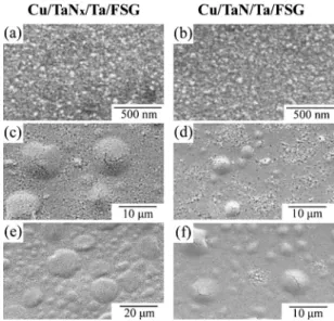
Figures 1 and 2 present the SEM micrographs on the surfaces of Cu/Ta–N/Ta/FSG/具Si典 and Cu/Ta–N/Ta/OSG/具Si典 samples, re-spectively. The photographs of Fig. 1a and b show that the surface of the as-deposited Cu films is principally smooth. The as-deposited Cu grains are rather small, and they comprise the nodules seen on
the surface. The SEM micrographs of the as-deposited
Cu/Ta–N/Ta/OSG/具Si典 samples are not shown in Fig. 2 because they are similar to those of as-deposited Cu/Ta–N/Ta/FSG/具Si典 samples. After annealing at 400°C, the Cu grains would grow in size for both systems 共Fig. 1c-f and 2a-d兲. Consequently,
the sheet resistance of the Cu/Ta–N/Ta/FSG/具Si典 and
Cu/Ta–N/Ta/OSG/具Si典 samples will decrease due to the reduction of the grain boundary and/or defect annihilation.21In addition,
ap-parently “bubblelike” features are observed on the surfaces of the Cu/Ta–N/Ta/FSG/具Si典 samples after annealing at 400°C for 30 or 60 min共Fig. 1c-f兲. The maximum dimension of the bubblelike fea-tures on the surface of Cu/TaNx/Ta/FSG/具Si典 after annealing at
400°C for 30 min is about 9.2m 共Fig. 1c兲 and then increases to 15.0m after annealing for 60 min 共Fig. 1e兲, while the average values of the bubble sizes are 8.3 and 12.8m, respectively. As for the Cu/TaN/Ta/FSG/具Si典 system, the sizes of the bubblelike
fea-tures are less than half of those appearing in the
Cu/TaNx/Ta/FSG/具Si典 system. This indicates that the maximum
di-mension of the bubblelike features on the surface of
Cu/TaN/Ta/FSG/具Si典 after annealing at 400°C for 30 min is about 4.4m 共Fig. 1d兲 and increases to 7.4 m after annealing for 60 min
共Fig. 1f兲, while the average values of the bubble sizes are 3.2 and
3.3m, respectively. On the contrary, Fig. 2 shows that the surface morphology of the Cu/Ta–N/Ta/OSG/具Si典 samples remains uni-form after annealing共Fig. 2a-d兲, although the Cu grains have grown in size. The significant divergence of the surface morphology on FSG/具Si典 and OSG/具Si典 substrates should be attributed to the differ-ent nature of the dielectric bottom layers.
The bubblelike morphology exhibited in the
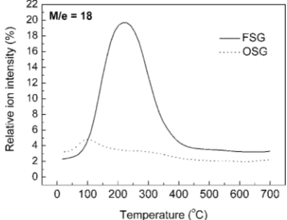
Cu/Ta–N/Ta/FSG/具Si典 system after annealing most likely can be attributed to the outgassing of dielectrics. FSG is essentially a fluorine-doped SiO2. The fluorine additives will reduce the dielectric constant and increase the porosity as well. Therefore, the as-deposited FSG film might absorb some gaseous matters and release them after annealing.22Since the released gases were capped with Cu/Ta–N/Ta overlayers, the top layers might deform in the local areas. Nevertheless, the Cu films deposited on OSG will not blister after annealing. To clarify if the bubblelike morphology was caused by outgassing from the dielectric layers, the dielectric films were analyzed by TDS. A constant heating rate of 20°C per minute was used during the measurement. The mass fragment of 18 M/e, corre-sponding to H2O, was measured; the TDS results of water desorp-tion from the FSG and OSG films are shown in Fig. 3.
In Fig. 3, the TDS spectra of the FSG and OSG films show apparently different behaviors. It had been reported that the water desorption peak at around 100°C was attributed to physically ab-sorbed water, while those at around 300°C were attributed to water molecules hydrogen bonded to isolated Si–OH bonds. In addition, water desorption above 350°C was attributed to constituent water.23 For the FSG film, a significant quantity of water evaporation was measured when the temperature reached 100°C and the amount of water desorption attained its maximum at 200–250°C. On the con-trary, for the OSG film the amount of the water evolution was much less than for the FSG film. Only a small desorption peak was
ob-Table I. Sheet resistances „in ⍀/䊐… of the Cu/Ta–N/Ta/dielectrics/ŠSi‹ samples, as deposited and after an-nealing at 400°C for 30 or 60 min.
As deposited 400°C-annealed for 30 min 400°C-annealed for 60 min Cu/TaNx/Ta/FSG/具Si典 0.227 0.127 0.122 Cu/TaN/Ta/FSG/具Si典 0.231 0.154 0.122 Cu/TaNx/Ta/OSG/具Si典 0.202 0.123 0.116 Cu/TaN/Ta/OSG/具Si典 0.216 0.125 0.116
Figure 1. SEM images on the surfaces of共a兲 as-deposited SEM images
Cu/TaNx/Ta/FSG/具Si典; 共b兲 as-deposited Cu/TaN/Ta/FSG/具Si典; 共c兲 400°C-annealed Cu/TaNx/Ta/FSG/具Si典 for 30 min; 共d兲 400°C-annealed Cu/TaN/Ta/FSG/具Si典 for 30 min; 共e兲 400°C-annealed Cu/TaNx/Ta/FSG/具Si典 for 60 min; and 共f兲 400°C-annealed Cu/TaN/Ta/FSG/具Si典 for 60 min.
Figure 2. SEM images on the surfaces of 共a兲 400°C-annealed Cu/TaNx/Ta/OSG/具Si典 for 30 min; 共b兲 400°C-annealed Cu/TaN/Ta/OSG/具Si典 for 30 min; 共c兲 400°C-annealed Cu/TaNx/Ta/OSG/具Si典 for 60 min; and 共d兲 400°C-annealed Cu/TaN/Ta/OSG/具Si典 for 60 min.
served primarily at 100°C for the OSG film. Furthermore, after an-nealing at 100°C, the water desorption from OSG decreased with increasing annealing temperature. Apparently, the FSG film absorbs many more water molecules than the OSG film does and releases the molecules strictly during annealing. In other words, OSG possesses better water absorption resistance than FSG does. The serious water adsorption/desorption behavior of FSG clearly explains the
bubble-like morphology seen on the surface of the annealed
Cu/Ta–N/Ta/FSG/具Si典 samples.
On the other hand, it had been reported that adhesion strength of the interface between Ta barrier and FSG film was poorer than that between Ta barrier and OSG film.24In this study, the adhesion of Cu/Ta–N/Ta multilayers on FSG and OSG was determined by using the Scotch tape test, and the result is shown in Table II. Each type of sample had been tested three times or more. The films of a particular type of sample, but on several specimens, were either all lifted or all firmly adhered. Therefore, the specimens that passed the test were marked as “䊊” or else marked as “⫻” in the table. Cu/FSG/具Si典 and Cu/OSG/具Si典 samples were also tested for reference. The table shows that all the Cu films deposited directly on the dielectrics
共including the FSG and OSG film兲 fail the test, both before and after
annealing. Meanwhile, the Cu/Ta–N/Ta multilayers deposited on the OSG films pass the test even after annealing at 400°C for an hour. However, the specimens in the Cu/Ta–N/Ta/FSG/具Si典 struc-ture fail the test after annealing. Figure 4 shows the cross-sectional SEM images of the Cu/Ta–N/Ta/FSG/具Si典 samples after annealing at 400°C for 60 min. It can be seen that the Cu/Ta–N/Ta layers peel at the Ta/FSG interface. This suggests, therefore, that the exposed surface, after the peeling test, should be the surface of the FSG layer. According to the results shown above, we can conclude that the Ta–N/Ta bilayers are effective adhesion promoters to enhance the adhesion strength between the as-deposited Cu layers and the low-k dielectrics共FSG and OSG兲, but not efficient for the samples with the FSG bottom layer after annealing. Iacopi et al. had reported
the formation of a Ta–C bond at the interface when Ta or Ta共N兲 compounds were deposited on a substrate containing carbon, which was the key reason for the improvement in adhesion.25On the other hand, the formation of the Ta–F bond did not enhance the adhesion and would even lower the adhesion strength.26,27 In the current study, the Ta layer in contact with the FSG film may react with the fluorine atoms and form Ta–F compounds, which would decrease the adhesion strength of the interface.
To confirm if the chemical interactions did occur at the interfaces between Ta and FSG, Ta–N and Ta layers, which were 5 and 2 nm in thickness, respectively, were deposited onto the FSG film and the chemical states on the surface were examined by using X-ray pho-toelectron spectroscopy. By using ultrathin Ta–N/Ta bilayers, we can detect the interfacial reaction because the detection depth of XPS is about 5–10 nm. Figure 5 shows the F 1s photoelectron spectra of the Ta–N共5 nm兲/Ta 共2 nm兲/FSG/具Si典 samples, as deposited and after annealing at 400°C for 60 min. No F signal was detected on the surface of the as-deposited Ta–N共5 nm兲//Ta 共2 nm兲/FSG/具Si典 specimens. However, after thermal treatment, the F 1s spectrum of the sample with TaNx
bar-rier shows a peak at 684.4 eV, which is associated with the Ta–F compound.28On the other hand, no peak could be found in the F 1s spectrum of the sample with TaN barrier. It has been reported that more nitrogen atoms would incorporate with tantalum atoms with increasing nitrogen flow ratios in the deposition process.29Thus, the significant reaction between TaNx共x ⬃ 0.5兲 and fluorine may be
attributed to the higher reactivity of Ta atoms in TaNxbecause they
are less bonded by nitrogen atoms. As a consequence, the “intrinsic” adhesion at the Ta/FSG interface of the Cu/TaNx/Ta/FSG sample should be worse than that of the Cu/TaN/Ta/FSG sample. Since the degree of outgassing from FSG should be independent of the cap
Figure 3. TDS spectra of FSG and OSG films in regard to the mass fragment
of 18 M/e共H2O兲.
Table II. Results of the adhesion test determined by Scotch tape test. The samples passing the test without peeling of the copper films are marked as “䊊,” or else marked as “ⴛ” in the table.
As deposited 400°C-annealed for 30 min 400°C-annealed for 60 min Cu/FSG/具Si典 ⫻ ⫻ ⫻ Cu/OSG/具Si典 ⫻ ⫻ ⫻
Cu/TaNx/Ta/FSG/具Si典 䊊 ⫻ ⫻
Cu/TaN/Ta/FSG/具Si典 䊊 ⫻ ⫻
Cu/TaNx/Ta/OSG/具Si典 䊊 䊊 䊊
Cu/TaN/Ta/OSG/具Si典 䊊 䊊 䊊
Figure 4. Cross-sectional images of scanning electron micrographs of共a兲
Cu/TaNx/Ta/FSG/具Si典 and 共b兲 Cu/TaN/Ta/FSG/具Si典 samples after anneal-ing at 400°C for 60 min.
Figure 5. XPS F 1 s spectra of共a兲 TaNx共5 nm兲/Ta 共2 nm兲/FSG/具Si典 and
共b兲 TaN 共5 nm兲/Ta 共2 nm兲/FSG/具Si典 samples, as deposited and after an-nealing at 400°C for 60 min.
layers, the overlayers with inferior intrinsic adhesion with FSG will become detached more easily when FSG outgases. Therefore, we observe larger blister size in the annealed Cu/TaNx/Ta/FSG sample
共Fig. 1e兲 than in the annealed Cu/TaN/Ta/FSG sample 共Fig. 1f兲.
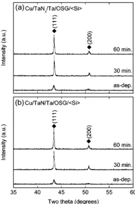
Figures 6 and 7 present a series of XRD patterns of Cu/Ta–N/Ta/FSG/具Si典 and Cu/Ta–N/Ta/OSG/具Si典 samples, before and after annealing at 400°C for 30 or 60 min, respectively. In these figures, the diffraction peaks of the as-deposited copper are broad in shape in both the FSG and OSG systems, indicating that the as-deposited Cu layers have rather small crystal grains. After annealing at 400°C in vacuum for 30 or 60 min, the Cu grains grow in size and the crystallinity of the Cu films will be enhanced. Consequently, the intensities of the Cu共111兲 diffraction peaks increase and the Cu共200兲 diffraction peaks will appear as well after annealing. Fig-ures 6 and 7 also show that Cu共111兲 preferred orientation exists in
both the Cu/Ta–N/Ta/FSG/具Si典 and Cu/Ta–N/Ta/OSG/具Si典
samples after annealing. As a result, the grain growth and develop-ment of crystal orientation for the copper layers are not strongly affected by the selection of barrier 共TaNx vs TaN兲 and dielectric
共FSG vs OSG兲 materials. Meanwhile, no new phases are found in
the XRD patterns of the Cu/Ta–N/Ta/low-k material/具Si典 samples, even after annealing at 400°C for 60 min. The chemical reaction occurring in the specimens upon annealing should be minuscule, or the reaction products are noncrystalline.
In summary, according to the experimental results shown above, substantial outgassing of FSG leads to the detachment of Cu/Ta–N/Ta multilayers from FSG. It is significant upon annealing, and blisters are seen on the annealed samples共Fig. 1c-f兲. Further-more, Ta–F compounds formed as the Ta or Ta–N layers deposited on the FSG film also result in the poor performance and reliability issue of the devices. On the other hand, no significant reactions could be observed in the Cu/Ta–N/Ta/low-k material/具Si典 structures by XRD, even after annealing at 400°C for 60 min. This indicates
that the Ta–N共10 nm兲/Ta 共2 nm兲 composite layers possess excel-lent diffusion barrier properties to prevent Cu from reacting with the underlayers after thermal treatment.
Conclusion
This study investigates the resistance and interfacial reactions of the Cu/Ta–N/Ta/low-k materials/具Si典 samples, before and after an-nealing at 400°C in vacuum for 30 or 60 min. Experimental results indicate, as compared to OSG, FSG outgases more significantly, and formation of Ta–F compounds is clearly detected in the TaNx/Ta/FSG interface. The outgassing of FSG will lead to
blister-ing of the Cu surface and degrade adhesion strength of Cu/Ta–N/Ta multilayers on FSG, while the formation of Ta–F will further en-hance the blister size on the surface of TaNx-barrier samples. On the contrary, the Cu/Ta–N/Ta multilayers deposited on OSG remain smooth and adhere well, even after annealing at 400°C for 60 min. Therefore, selection of dielectric and barrier materials is critical for the reliability of the copper metallization system. The current study suggests that OSG and TaN are the better choices as dielectric and barrier materials, respectively, owing to less outgassing of OSG as compared to FSG and lower chemical reactivity of TaN as compared to TaNx.
Acknowledgment
The authors gratefully acknowledge the financial support from the National Science Council of Taiwan共grant no. NSC-93-2216-E-006-015兲.
National Cheng Kung University assisted in meeting the publication costs of this article.
References
1. C. W. Park and R. W. Vook, Appl. Phys. Lett., 59, 175共1991兲. 2. P. J. Pan and C. H. Ting, IEEE Trans. Ind. Electron., IE-29, 154共1982兲. 3. C. S. Liu and L. J. Chen, J. Appl. Phys., 74, 5001共1993兲.
4. S. P. Murarka, Mater. Sci. Eng., R., 19, 87共1997兲.
5. K. M. Chang, T. H. Yeh, I. C. Deng, and C. W. Shih, J. Appl. Phys., 82, 1469 Figure 6. XRD patterns of 共a兲 Cu/TaNx/Ta/FSG/具Si典 and 共b兲
Cu/TaN/Ta/FSG/具Si典 samples, before and after annealing at 400°C in vacuum for 30 or 60 min.
Figure 7. XRD patterns of 共a兲 Cu/TaNx/Ta/OSG/具Si典 and 共b兲 Cu/TaN/Ta/OSG/具Si典 samples, before and after annealing at 400°C in vacuum for 30 or 60 min.
共1997兲.
6. A. Broniatowski, Phys. Rev. Lett., 62, 3074共1989兲.
7. M. J. Shapiro, S. V. Nguyen, T. Matsuda, and D. Dobuzinsky, Thin Solid Films,
270, 503共1995兲.
8. M. J. Loboda, Microelectron. Eng., 50, 15共2000兲.
9. M. Moriyama, T. Kawazoe, M. Tanaka, and M. Murakami, Thin Solid Films, 416, 136共2002兲.
10. H. C. Chen, B. H. Tseng, M. P. Houng, and Y. H. Wang, Thin Solid Films, 445, 112
共2003兲.
11. K. P. Yap, H. Gong, J. Y. Dai, T. Osipowicz, L. H. Chan, and S. K. Lahiri, J.
Electrochem. Soc., 147, 2312共2000兲.
12. G. S. Chen and S. T. Chen, J. Appl. Phys., 87, 8473共2000兲.
13. K. M. Latt, Y. K. Lee, S. Li, T. Osopowicz, and H. L. Seng, Mater. Sci. Eng., B,
84, 217共2001兲.
14. M. Hecker, D. Fischer, V. Hoffmann, H.-J. Engelmann, A. Voss, N. Mattern, C. Wenzel, C. Vogt, and E. Zschech, Thin Solid Films, 414, 184共2002兲.
15. M. Uekubo, T. Oku, K. Nii, M. Murakami, K. Takahiro, S. Yamaguchi, T. Nakano, and T. Ohta, Thin Solid Films, 286, 170共1996兲.
16. A. E. Kaloyeros and E. Eisenbraun, Annu. Rev. Mater. Sci., 30, 363共2000兲. 17. B. H. Lee and K. Yong, J. Electrochem. Soc., 151, C594共2004兲.
18. Z. Wang, T. Ida, H. Sakaue, S. Shingubara, and T. Takahagi, Electrochem.
Solid-State Lett., 6, C38共2003兲.
19. International Technology Roadmap for Semiconductors, Semiconductor Industry Association, update 2003.
20. C. C. Chang, J. S. Jeng, and J. S. Chen, Thin Solid Films, 413, 46共2002兲. 21. A. F. Mayadas and M. Shatzkes, Phys. Rev. B, 1, 1382共1970兲.
22. M. J. Shapiro, T. Matsuda, S. V. Nguyen, C. Parks, and C. Dziobkowski, J.
Elec-trochem. Soc., 143, L156共1996兲.
23. N. Hirashita, S. Tokitoh, and H. Uchida, Jpn. J. Appl. Phys., Part 1, 32, 1787
共1993兲.
24. G.-R. Yang, Y.-P. Zhao, B. Wang, E. Barnat, J. McDonald, and T.-M. Liu, Appl.
Phys. Lett., 72, 1846共1998兲.
25. F. Iacopi, Zs. Tökei, Q. T. Le, D. Shamiryan, T. Conard, B. Brijs, U. Kreissig, M. Van Hove, and K. Maex, J. Appl. Phys., 92, 1548共2002兲.
26. G. Passemard, P. Fugier, P. Noel, F. Pires, and O. Demolliens, Microelectron. Eng.,
33, 335共1997兲.
27. S. H. Yang, H. Kim, and J. W. Park, J. Vac. Sci. Technol. A, 20, 1769共2002兲. 28. J. P. Chang, H. W. Krautter, W. Zhu, R. L. Opila, and C. S. Pai, J. Vac. Sci. Technol.
A, 17, 2969共1999兲.
29. J. H. Wang, L. J. Chen, Z. C. Lu, C. S. Hsiung, W. Y. Hsieh, and T. R. Yew, J. Vac.