國立交通大學
電子工程學系電子研究所
碩士論文
應用寫入輔助電路之低功耗雙埠
靜態隨機記憶體之測試方法
Test Methodology for
Low-Power Dual-Port SRAM Utilizing Write-Assist Cells
Against Simultaneous Access Disturbance
研究生:黃召穎
指導教授:趙家佐
測
應用寫入輔助電路之低功耗雙埠
靜態隨機記憶體之測試方法
Test Methodology for
Low-Power Dual-Port SRAM Utilizing Write-Assist Cells
Against Simultaneous Access Disturbance
研究生:黃召穎
Student:Chao-Ying Huang
_____
指導教授:趙家佐 Advisor:Mango Chia-Tso Chao
國立交通大學
電機學院 電子工程學系 電子研究所
碩士論文
A Thesis
Submitted to Department of Electronics Engineering & Institute of Electronics College of Electrical and Computer Engineering
National Chiao Tung University In partial Fulfillment of the Requirements
for the Degree of Master
in
Electronics Engineering August 2013
Hsinchu, Taiwan, Republic of China
I
應用寫入輔助電路之低功耗雙埠
靜態隨機記憶體之測試方法
研究生:黃召穎 指導教授:趙家佐
國立交通大學
電機學院 電子工程學系 電子研究所
摘要
隨著多核心運算及平行化處理需求漸增,雙埠靜態隨機記憶體在提高效 能上的優勢逐漸顯著.另一方面由於記憶體應用層面逐漸由傳統桌上型電 腦轉移到行動裝置等相關產品,因此以低功耗操作和高速存取為目標的記 憶體設計更是蓬勃發展.然而在先進製程中嚴重製程變異使製造過程中的 穩定性相對降低,以及在追求低功耗操作及高速的存取的情況下,雙埠靜 態隨機記憶體的的讀取及寫入更加顯得不穩定.上述的不穩定性導致雙埠 隨機靜態記憶體在低功耗操作上更顯困難.為了保持可接受的讀取及寫入 能力配合降低操作電壓達到低功耗的目的.許多讀取及寫入的輔助電路在 各個製程下逐漸被提出使用.本論文著重於討論雙埠靜態隨機記憶體配合 寫入輔助電路幫助下之開路缺陷的錯誤行為模式並提出相對應的測試方法. 此輔助電路應用於解決雙埠靜態隨機記憶體在先進製程下受到嚴重製程變 異使寫入能力衰減嚴重的情況.II
Test Methodology for
Low-Power Dual-Port SRAM Utilizing Write-Assist Cells
Against Simultaneous Access Disturbance
Student:Chao-Ying Huang
Advisor:Mango Chia-Tso Chao
Department of Electronics Engineering and Institute of
Electronics National Chiao-Tung University
Abstract
With the increasing demand of parallel applications and multi-core operations, the advantages of Dual-Port SRAMs have become more important. Also, applications of SRAMs have moved from the traditional desktop to the mobile device; therefore, the designs which are aimed at low-power operations and high-speed accesses are currently prospering. Besides as process variation in the advanced technology becomes more severe, the stability of SRAMs in data retention mode and read/write operation has become more fragile. The low stability property may cause Dual-Port SRAMs unable to operate at low voltage. In order to maintain an acceptable read/write margin with low power issue, some read/write assist circuitries have been proposed recently. As a result, the thesis emphasizes on the fault behaviors of open defects for Dual-Port SRAMs with specific write-assist circuitry and its corresponding test methodologies for those hard-to-detect faults.
III
Acknowledgements
First and foremost, I would like to express my greatest appreciation to my advisor, Professor Chia-Tso Chao (Mango, 趙家佐). He is not only a teacher but also a life mentor to me. He is always there when I am at the crossroad of my life, and guides me with clear and useful advices. He expects me to be a man not only with professional skills but with a positive attitude toward challenges. I would never become who I am today if it were not for him. It is my honor to meet a friend-like teacher as Professor Chao. Second, I’d like to thank my upperclassmen, Jhen-An Lai. He gives me opportunities to work as an intern in TSMC and helps me get over the difficulties in this work. Everything I learned from him is a great treasure in my life. I will always keep that in mind and be thankful forever. Third, I’d like to thank my lab-mates: Hao-Yu Yang, Cheng-Wei Lin, Sz-Pang Mu, Yu-An Chen and all the others. Without their assistance, I would not be able to deal with the academic works and the arduous research tasks smoothly during the past two years. Last, I appreciate my dear parents and my girlfriend, Michelle, for their support and encouragement all these years. It is your immense love that keeps me fighting hard. I hope that this work makes you proud.
Chao-Ying Huang National Chiao-Tung University
IV
Contents
中文摘要 I English Abstract II Acknowledge III List of Tables VI List of Figures VII1 Introduction ………1
2 Write-Assist Dual-Port SRAM and the Fault Behaviors ………3
2.1 Background of Write-Disturb Issue ……….5
2.2 Write-Assist Circuitry and Its Operations ……….8
2.2.1. Background of Write-Assist Circuitry ………8
2.2.2. Write-Assist Circuitry Operations ……….9
2.2.3. Write-Assist Circuitry Control ………10
2.3 Fault Behaviors of DP-SRAMs and Write-Assist Circuitry ……11
2.3.1 Background of Stability Faults ………11
2.3.2 Macro Implementation ………12
2.3.3 Fault Behavior for Dual-Port SRAM Cells ………13
2.3.4 Fault Behaviors for Write-Assist Circuitry……….20
3 Testing of Write-Assist Dual-Port SRAM and the Proposed Methods ……22
3.1 Testing of the Open Defects in Dual-Port SRAM Core Cell …………23
3.1.1 Previous Method – Severe Write Method ………...23
3.1.2 Proposed Method – Half-VDD Attacking Method ……25
3.1.3 Experiment Results and Comparison ………26
3.2 Testing of the Open Defects in Write-Assist Circuitry ………29
V
3.2.2 Proposed Method – Severe Read Method ………30
3.2.3 Experiment Results and Comparison ………31
3.3 Design-for-Test for the Proposed Methods ………...33
3.3.1 DFT for Half-VDD Attacking Method ………...33
3.3.2 DFT for Low-V Write-Assist Enable Method …………35
4 Conclusion ……….37
VI
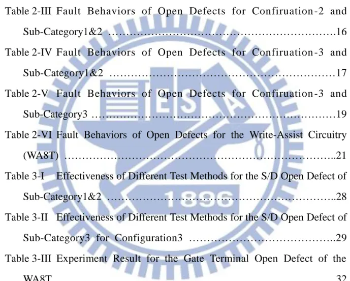
List of Tables
Table 2-I Cross Combinations of Different Discussed Conditions ………13 Table 2-II Fault Behaviors of Open Defects for Confiruation -1 and Sub-Category1&2 ………16 Table 2-III Fault Behaviors of Open Defects for Confiruation -2 and Sub-Category1&2 ……….16 Table 2-IV Fault Behaviors of Open Defects for Confiruation -3 and Sub-Category1&2 ………17 Table 2-V Fault Behaviors of Open Defects for Confiruation -3 and Sub-Category3 ………19 Table 2-VI Fault Behaviors of Open Defects for the Write-Assist Circuitry (WA8T) ………..21 Table 3-I Effectiveness of Different Test Methods for the S/D Open Defect of Sub-Category1&2 ………..28 Table 3-II Effectiveness of Different Test Methods for the S/D Open Defect of Sub-Category3 for Configuration3 ………..29 Table 3-III Experiment Result for the Gate Terminal Open Defect of the WA8T ………32 Table 3-IV Experiment Result for the S/D Terminal Open Defect of the WA8T ………33 Table 3-V Half-VDD Attacking Operating Flow ………34 Table 3-VI Comparisons of Voltage State for Half-VDD Attacking …………35 Table 3-VII Operations of Low-V Write-Assist ………36
VII
List of Figures
Fig. 2-1 Illustration of DP-SRAM and VDDmin Penalty [2-1] ………5
Fig. 2-2 Waveform of Write Disturbance [2-1] ………6
Fig. 2-3 Waveform of Write Disturbance for Different Skews [2-4] …………7
Fig. 2-4 Structure and Schematic of DP-SRAM and the WA8T [2-1] …………8
Fig. 2-5 Simulated Waveform of the W-R Operation [2-1] ………10
Fig. 2-6 Illustration Waveform of the WAEN Signal ………10
Fig. 2-7 Schematic of Dual-Port SRAM Cell ………14
Fig. 2-8 Schematic of the Write-Assist Circuitry (WA8T) ………20
Fig. 3-1 Illustration of Severe Write Method[2-11] ………...24
Fig. 3-2 Illustration of Half-VDD Attacking Method ………26
Fig. 3-3 Illustration of Severe Read Method ………..31
Fig. 3-4 Illustration of the DFT for Half-VDD Attacking ………34
1
Chapter 1
Introduction
Parallelism has been the one of the most important principles to increase a system’s throughput in the past. With the continually decreasing price and increasing performance of silicon chips for each new process generation, incorporating multiple processors into a system has become a more feasible, effective, and economic solution to further explore the computation parallelism of a system as well as its throughput. The performance of a multiple-core system can be significantly affected by the following two major factors: (1) the bandwidth of its memory and (2) the bandwidth of its communication between different cores. To improve the memory bandwidth and the communication bandwidth, significant research efforts have been put into the area of multi-port SRAM designs and network-on-chip (NOC) designs in the past, respectively. Designing a multi-port SRAM to provide multiple paralleled accesses to the same data array is an effective solution to increase the memory bandwidth. Dual-port SRAMs are the most commonly used multi-port SRAMs nowadays, providing two individual ports which can perform either a read or a write operation independently.
On the other hand, due to the increasing demand of low-power system, a great amount of research effort has been spent in the past to develop the effective and economic designs so as to operate with low supply voltage.
2
However, Dual-Port SRAMs suffer disturb issues in advanced technology nodes owing to its dual-port access nature. These disturb issues may degrade the minimum operating voltage of Dual-Port SRAMs. Therefore, many read-/write- assist circuits have been proposed to circumvent these disturb issues. Accordingly test methods regarding those newly developed Dual-Port SRAM designs and assist circuitries have not been fully discussed yet.
In the chapter 2, we first discuss the reasons that cause the write disturbance for Dual-Port SRAMs in detail and we talk about the write-assist circuitry used in this work later, including the basic operation of it and its timing controls. We then move to the discussion of defect injection part. We show the experiment results of the measured resistance for each open defect from the table 2-I to the table2-V. By observing the results, we aim our targets at the larger resistance detects and we propose our own test methodologies in the next chapter.
In the chapter 3, we introduce the previous methods proposed by others that relate to our targets and our proposed method as well. The followings are our proposed methods. Half-VDD attacking method is used for the defects in Dual-Port SRAM Cell and low-voltage write-assist method and severe read method are used for the defects in the write-assist circuitry independently. Later, we show the comparison table of the measured results to prove that our methods are in good use. In the end, we discuss Design-For-Test of the proposed methods to prove that our methods are applicable. In the chapter 4, we make a brief conclusion about our work. In chapter 5, we talk about the future work of this research.
3
Chapter 2
Write-Assist Dual-Port SRAM and the Fault
Behaviors
In deep sub-micrometer technology, system-on-chip (SoC) products require a high-speed and low-power embedded memory to support increased storage capability. Therefore, dual-port static random access memory (DP-SRAM) has been widely used for SoC products such as graphic and media processing chips. In order to obtain low-power target, low supply voltage method has been widely used for these advanced applications. However, utilizing low supply voltage to achieve power reduction for DP-SRAMs is susceptible to variations in the threshold voltage (VTH). These variations might result from random doping
fluctuations and lithography processes, which cause a subsequent reduction in the VDDmin performance of SRAMs. For DP-SRAMs, the VDDmin is even more
fragile when discussing whether one- or two- port operation is enabled, especially when it is operated at the dual-port access. In this chapter we will discuss the background of DP-SRAM operations and the write-disturb issue. We implement the DP-SRAM macro and observe the repairing mechanism of the write-assist circuitry at first. Then we analyze the effects causing by the open defect on the gate or the source/drain terminal later.
Figure 2-1(a) shows a schematic of the DP-SRAM. There are two different word-lines (AWL and BWL) controlling different-port operations. For each
4
operation, they determine the corresponding electrical connection between storage nodes (Q and QB) and bit-line pairs (ABL/ABLB and BBL/BBLB). A DP-SRAM macro has two independent timing control circuits and address decoders respectively and these two independent ports can be operated simultaneously. Hence, DP-SRAMs suffer “disturb issue” when both ports are accessed at the same row. The disturb issue can be classify into read-disturb issue and write-disturb issue. The extent of each disturb issue is related to the timing skew of different clock phase. Figure 2-1(b) shows that the worst Vmin
condition occurs when some clock difference exists. In this work, we focus on write disturb issue which has more severe VDDmin degradation problem in short
word-line pulse for high speed applications.
From Figure2-1 (b), the positive timing skews (Tsk) happen when activating
the write word-line before the read word-line (W-R operation) and it causes a great degradation in VDDmin; in contrast, the negative timing skews (Tsk) happen
when activating the read word-line before write word-line (R-W operation) and it causes no clear degradation in VDDmin. For this reason, W-R operation in the
same row is the major concern for the write-disturb issue.
To overcome the disturb issue and successfully operate DP-SRAMs at lower VDDmin, some new assist circuitry designs for read or write operations have
been proposed. Tackling the read-disturb issue, which causes degradation in read static noise margin on 65nm technology node, [2-2] proposed a bit-line shifter circuit and row address comparator to prevent common-row-access operation. For the write-disturb issue, [2-1], [2-3] and [2-5] proposed the write-assist circuit to achieve a lower VDDmin with low area overhead and power
consumption on either 45nm or 28nm technology node. [2-4] even analyzed the read-/write- disturb issue under different timing skews and proposed a screening
5
circuitry to allow us to generate the read-/write- disturb condition without conventional costly operations. We select [2-1] as the write-assist circuitry in the following work, because it is not only the newest write-assist circuitry but with minimum area overhead as well.
Fig. 2-1 Illustration of DP-SRAM and VDDmin Penalty [2-1]
2.1 Background of Write-Disturb Issue
When VTH variations happen, the unbalanced driving ability of cross-couple
inverter and pass-gate transistors of DP-SRAM cell may make the cell prefer to
(a) Cell Structure of the DP-SRAM cell
6
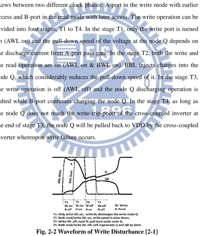
specific read or write operation. This situation is even more severe in advanced process, such as 40nm or 28nm technology. Moreover, simultaneous row access behaviors degrade the read/write margin seriously and the synchronization of the timing of different word-lines is also important in low supply voltage condition.
Figure 2-2 shows a simulated waveform of DP-SRAM cell storing logic-1 under A-port write and B-port read operation (W-R). There exist some timing skews between two different clock phases: A-port in the write mode with earlier access and B-port in the read mode with later access. The write operation can be divided into four stages, T1 to T4. In the stage T1, only the write port is turned on (AWL on) and the pull-down speed of the voltage at the node Q depends on the discharge current from A-port pass gate. In the stage T2, both the write and the read operation are on (AWL on & BWL on). BBL injects charges into the node Q, which considerably reduces the pull-down speed of it. In the stage T3, the write operation is off (AWL off) and the node Q discharging operation is halted while B-port continues charging the node Q. In the stage T4, as long as the node Q does not reach the write-trip-point of the cross-coupled inverter at the end of stage T3, the node Q will be pulled back to VDD by the cross-coupled inverter whereupon write failure occurs.
7
The timing skews between different word-lines are also important for the write-disturb issue. Figure 2-3 shows the comparison waveform of the timing skews for the simultaneous row access of DP-SRAM cell. The notation MT and MB stand for two complementary storage nodes. A-port is for write-logic-0 operation and B-port is for read-operation (or half-selected read) in this example. Figure 2-3(a) corresponds to negative skews, figure 2-3(b) corresponds to zero skew, figure 2-3(c) corresponds to positive skews and figure 2-3(d) corresponds to amount of positive skews between word-lines. Regarding figure 2-3(a) and figure 2-3(b), although the MT suffers the write-disturb issue, the write operation is success owing to its inherent cell ability to flip the internal data. However, in figure 2-3(c), the MT is kept on ramping up by BLB after WLA is off, which eventually results in the write failure. With regard to figure 2-3(d), where the amount of positive skew is larger than figure 2-3(c), MT flips immediately because the write-disturb issue starts appearing after the write operation is finished. To sum up, figure 2-3(c) produces the worst-case scenario, which needs effective write-assist circuitry to repair during the write operation.
Fig. 2-3 Waveform of Write Disturbance for Different Skews (a) negative skew (b) zero skew (c) positive skew (d) amount of positive skew [2-4]
8
2.2 Write-Assist Circuitry and Its Operation
2.2.1 Background of Write-Assist Circuitry
Figure 2-4 shows the structure of DP-SRAM using the proposed write-assist circuitry from [2-1], which is noted as the WA8T cell. It achieves a lower VDDmin by suppressing the write disturbance with small area overhead and low
power consumption. The circuitry is formed by two inverters (INV1 and INV2) and two stacked-NMOS bit-line pull down drivers (N1-N2 and N3-N4 pairs). The write-assist enable signal (WAEN) controls the N1 and N3 transistor to determine when the WA8T cell should be turned on.
According to [2-1] states, SRAMs usually require edge dummy cells to ensure a uniform layout in the middle and edges of the cell array. The proposed WA8T cell uses the poly and diffusion layout pattern of regular DP-SRAM cells, which facilitates the proximity effect of the DP-SRAM edge dummy cells. Therefore, with cells placed in the same locations along the top/bottom edge of dummy cells, the proposed the WA8T cell has almost no area penalty.
9
2.2.2 Write-Assist Circuitry Operations
Figure 2-5 shows an example that how the WA8T cell helps to suppress the write disturbance through a W–R operation in DP-SRAM cell. In the operation, two word-lines are accessed at the same row with independent operations: A-port is for write-logic-0 and B-port is for read operation (or half-selected read). ABL is pulled down to ground and ABLB is maintained at VDD by the write driver of A-port, while both BBL and BBLB are at VDD at the beginning of BWL. It can be seen that DP-SRAMs without the WA8T cell may suffers the write-disturb issue causing write-logic-0 operation failed at the end of AWL. Eventually, cross-couple inverters pull back the node Q to VDD resulting in the write failure.
On the other hand, DP-SRAMs with the WA8T cell would pass the write operation under the write-disturb issue. The INV1 senses the logic-0 at ABL and outputs a logic-1 at the gate of N4. The INV1 senses the logic-1 at ABLB and outputs a logic-0 at the gate of N2. When the WAEN signal for A-port WA8T cell is active, the N3–N4 stacked-NMOS driver begins discharging BBL and the N1–N2 driver is in a state of high impedance (N2 is off). The B-port WA8T cell remains inactive by keeping its WAEN signal off. The reduced voltage at BBL helps to suppress the write disturbance caused by B-port being pulled high in the conventional approach. Moreover, the WA8T cell not only suppresses the write-disturb issue but also improves the write margin owing to the additional write path of the other port (B-port in this example).
10
Fig. 2-5 Simulated Waveform of the W-R Operation [2-1]
2.2.3 Write-Assist Circuitry Control
The write-assist enable signal (WAEN) of the WA8T cell is implemented in the A-/B- port timing control circuits independently. Figure 2-6 illustrates the timing of the WAEN signal. The WAEN signal remains at logic-0 level (inactive) under all conditions except the W–R operation at the same row. Moreover, if AWL and BWL are in the non-overlapping region, the WAEN signal also remains at logic-0 level even for the W–R operation. Note that the WA8T cell should be disabled (WAEN = logic-0) for the R–W operation. If the WA8T cell is activated during the R–W operation (B-port read and A-port write), the WA8T cell will transfer the B-port read data to the ABL and the ABLB, resulting in data conflict.
AWL
BWL
WAEN
11
2.3 Fault Behaviors of DP-SRAMs and Write-Assist Circuitry
2.3.1 Background of Stability Faults
A stability fault defined in [2-6]-[2-7] refers to a small open defect on the source/drain terminal of four cross-coupled transistors, which may not fail a read or a write operation under a typical operating condition but may fail under some corner conditions (such as significant IR drop, noise, or soft error). As a result, a stability fault may decrease the reliability of SRAM but may not be easily detected by a conventional march sequence. Therefore, testing stability faults has become one of the most challenging tasks in current SRAM testing. Several test methods were proposed to detect the stability faults with as small resistance as possible, [2-6]-[2-9].
For traditional 6T SRAMs, the past research effort mainly focused on the stability faults located on the source/drain terminal of pull-up PMOS transistors and ignored the stability faults locating on pull-down NMOS transistors, which can be detected relatively easily by the read operation because the bit-lines in general SRAMs operations are pre-charged to VDD before a read operation. If the NMOS transistors cannot successfully pull down the bit-line due to the open defects, the pre-charged value (floating logic-1) will be read out, which is opposite to the expected value. On the other hand, if the PMOS transistors cannot successfully pull up the bit-line due to an open defect, the pre-charged value (floating logic-1) just happens to be the expected value making the open defect not detect.
For DP-SRAMs, [2-10] states that it can be divided into single-port faults (1PFs) and two-port faults (2PFs). The 1PFs can be detected using the
12
conventional single port memory tests. However, through our experiment, we found that open defects for stability faults located on the source/drain terminal of pull-up PMOS transistors are still hard to detect. We focus on 1PFs in the following part and the 2PFs requiring special test methods are not involved in this work.
2.3.2 Macro Implementation
We implement a DP-SRAM macro on 28nm technology node with 128 cells per column and per row. The sizing of the DP-SRAM cell is based on [2-2] so as to make the cell with weak read-ability and weak write-ability. The capacitance on each bit-line is 20 fF, which is suggested by our cooperated industries. We use 2-stage row decoder and mux8 tree-based column decoder. The sense amplifier we use is a latch type sense amplifier. We operate the macro at 0.75V which is lower than its standard supply voltage, 1.05V, to realize low power application. As stated before, the write-disturb issue occurs when there exists variations in threshold voltage (VTH) and some positive word-line skews.
Therefore, we carry out three different cell-sizing and run Monte-Carlo simulations to verify that for each cell-sizing the single-port access can work successfully and the simultaneous dual-port access would fail. In order to observe the open defects in the WA8T cell, we select seven VTH variation
conditions on cell-sizing-3 and use the WA8T cell to repair the write-disturb issue as stated in [2-1]. For both the DP-SRAM macro and the WA8T cell, we proceed to perform the defect injection exhaustively and use different test methods to detect the minimum resistance.
13
The experiments can be divided into two main categories: Category1: Open Defects occur in DP-SRAM cell.
Category2: Open Defects occur in the WA8T cell.
The category1 can be divided into three sub-categories. Each sub-category represents one cross-combination of with/without VTH variation and
with/without the WA8T cell in table 2-I. We do not discuss the situation when DP-SRAMs with VTH variations and without write-assist circuitry
simultaneously, because DP-SRAMs can not operate correctly even for defect free condition.
TABLE 2-I
Cross Combinations of Different Discussed Conditions
w/ VTH Variations w/o VTH Variations
w/ Write-Assist Circuitry Sub-category3 Sub-category2 w/o Write-Assist Circuitry Not in discussion Sub-category1
2.3.3 Fault Behaviors for Dual-Port SRAM Cells
In the following experiments, we inject an open defect with different resistance value one at a time on each terminal (gate or source/drain) of each transistor, as shown Figure 2-7. By sweeping all single-port read/write operations and all dual-port write-read operations, we report the minimum resistance for each open defect, which can cause a fault behavior for DP-SRAM design, shown in table 2-II to Table 2-IV. In order to observe whether the open defect for DP-SRAM cells will be affected by the VTH variation and the WA8T
14
discuss experiment results of sub-category1 and sub-category2 together to compare the influence of with/without write-assist circuitry and then we discuss the sub-category3 to compare the influence of different VTH variations in cell-sizing-3.
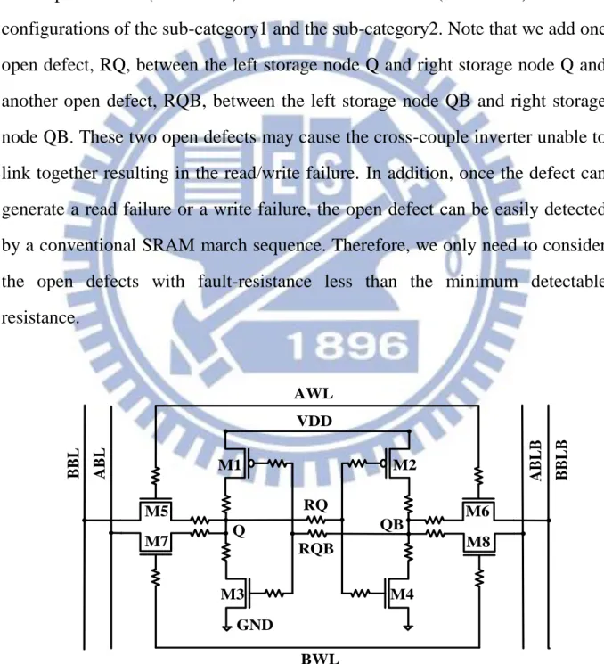
From Table 2-II to Table 2-IV list the minimum detectable resistance of each open defect (Column 5) and the fault behavior (Column 4) for three configurations of the sub-category1 and the sub-category2. Note that we add one open defect, RQ, between the left storage node Q and right storage node Q and another open defect, RQB, between the left storage node QB and right storage node QB. These two open defects may cause the cross-couple inverter unable to link together resulting in the read/write failure. In addition, once the defect can generate a read failure or a write failure, the open defect can be easily detected by a conventional SRAM march sequence. Therefore, we only need to consider the open defects with fault-resistance less than the minimum detectable resistance. A B L BWL AWL B B L A B L B B B L B VDD M1 M3 M2 M4 RQ RQB Q QB M5 M7 M6 M8 GND
15
We demonstrate that the open defects located on the DP-SRAM cell (M1 to M8) all fail on the single-port or the dual-port write operation from Table 2-II to Table 2-IV. These defects are classified as stability faults in Section 2.3.1. Apparently, the open defects located on the gate terminal are detected by a larger resistance. We infer that it is mainly related to its inherent high impedance nature of the device structure. On the contrary, most open defects locate on the source/drain terminal are easy to detect except those on the source/drain terminal of the pull-up transistors. Similar to traditional 6T SRAMs, stability faults on PMOS transistors (M1 and M2) are hard to detect and stability faults on NMOS transistors can be detected with two-order less for category-1 and category-2. This result states that detecting stability faults on PMOS transistors is more critical than on NMOS transistors for DP-SRAM cell without VTH
variations. From Table 2-II to Table 2-IV, we note that category-1 and category-2 have similar minimum detectable resistance for each open defect. We can conclude that the write-assist circuitry has no great influence on testing DP-SRAM cells with little or no VTH variations.
16
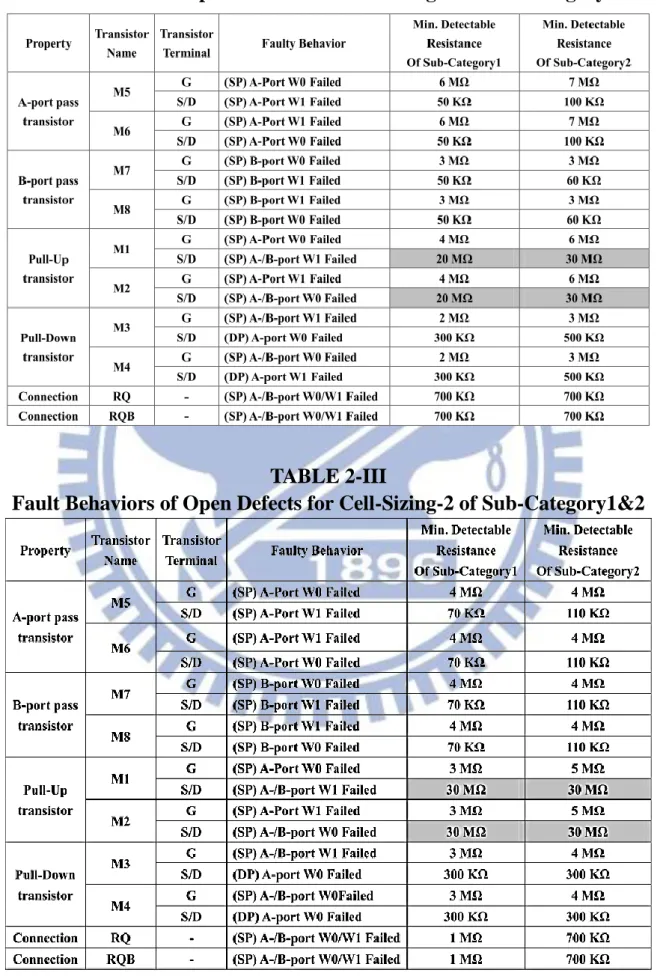
TABLE 2-II
Fault Behaviors of Open Defects for Cell-Sizing-1 of Sub-Category1&2
TABLE 2-III
17
TABLE 2-IV
Fault Behaviors of Open Defects for Cell-Sizing-3 of Sub-Category1&2
For the sub-category3, we select cell-sizing-3 as the base macro circuit and run Monte-Carlo simulations. There are eight groups of VTH variation and each
of them implements the dual-port A-port write-logic-1 and the B-port read-logic-0 operation simultaneously so that DP-SRAM cell suffers the write-disturb issue. Table 2-IV shows the minimum detectable resistance of each open defect (from Column 5 to Column 12) and the preferred test operations (Column 4) for configuration-3 of the sub-category3. The preferred test operations in this table simply note single- or dual- port write operation without detail. It is because each open defect of each VTH variation has its preferred test
operations; therefore, it’s too complicated to include them all.
Table 2-IV shows that the trend for DP-SRAM cells with VTH variations and
18
previous results. In this experiment, it appears that only the open defect on the source/drain terminal of the left pull-up PMOS (M2) are hard to detect and others are relatively easy to detect by the conventional march test. We infer that it is due to the asymmetric VTH characteristic of the transistor in DP-SRAM cell.
The asymmetric behavior in this experiment makes the DP-SRAM cell tends to have the dual-port A-port write-logic-1 disturbance easily. In this way M1 PMOS becomes much weaker comparing to M2 PMOS; as a result, the open defect on the source/drain terminal of M1 becomes easier to detect.
19
TABLE 2-V
20
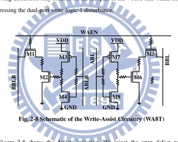
2.3.4 Fault Behaviors for Write-Assist Circuitry
In the following experiment, we focus on the open defects for the write-assist circuitry. The structure of the WA8T cell in Figure 2-8 is symmetric. The left part works for the dual-port A-port write-logic-1 operation and the right part works for the dual-port A-port write-logic-0 operation. As a result, the following discussion only focuses on the left part of the WA8T cell which helps suppressing the dual-port write-logic-1 disturbance.
B B L B M1 M2 M5 M6 B B L WAEN M4 M3 A B L B VDD GND M8 M7 VDD GND A B L
Fig. 2-8 Schematic of the Write-Assist Circuitry (WA8T)
Figure 2-8 shows the defects injection. We inject the open defect with different resistance value one at a time on each terminal (gate or source/drain) of each transistor (M1 to M4). Specially, M1 and M2 share the same resistance as their source/drain open defect. We report the minimum resistance for each open defect under seven VTH variations in table 2-V. These open defects can cause the
WA8T cell breaks down and hinder the suppression of the write-disturb issue of DP-SRAM cell.
21
As table 2-V shows, four open defects highlighted in the gray background are classified as hard to detect faults. Among these four open defects, three of them are on the gate terminal and they are inherently high impedance. The other one is on the source/drain terminal of M4. As a result, we focus on developing test methods for the one on the source/drain terminal first and developing other methods to detect those hard to detect faults last.
TABLE 2-VI
22
Chapter 3
Testing of Write-Assist Dual-Port SRAM and
the Proposed Methods
A significant amount of research effort has been put into the area of developing an effective and economic DP-SRAM designs. Consequently, testing of DP-SRAMs has also become more important. In 2002, [2-10] has discussed realistic fault models for DP-SRAMs and it divided them into single-port faults and faults unique for dual-port operations. It concerns about faults that related to the multi-port and simultaneous access behavior for different cells. It states that testing multi-port memories require special tests since the multi-port and simultaneous access can sensitize faults that are different from conventional single-port memory faults.
However, such models become insufficient in deep sub-micrometer technology. We are more interested in the open defects that originate from manufacturing process. The existing testing methodologies are not effective enough for the advanced DP-SRAM design and the new write-assist circuitry and they have not been fully discussed in the literature yet. In this chapter, we will propose several test methods and each method is primarily used for one specific hard-to-detect fault in the chapter2. We develop these methods based on other’s works and the dual-port characteristic of DP-SRAMs. In this way, we can reduce the complexity of its DFT. We then compare experiment results to
23
prove that our methods are in good use. In the end of this chapter, we show the Design-for-Test (DFT) for each different test method.
3.1 Testing of the Open Defects in Dual-Port SRAM Core Cell
In this section, we first discuss the severe write method proposed in [2-11]. In our experiments, we found that this method is not useful when testing DP-SRAMs. We propose Half-VDD Attacking Method based on the severe write method to detect the stability faults. It turns out our method is useful for both DP-SRAMs with VTH variations and without VTH variations.
3.1.1 Previous Method – Sever Write Method
The idea of severe write method [2-11] in 6T SRAM design is performing a write operation by a weaker bit-line supply. Taking write-logic-0 as an example shown in figure 3-1(a), we set BL to strong logic-0 and BLB to floating logic-0 at the test mode (write logic-0 operation) instead of strong logic-0 and strong logic-1 at the normal mode. With such a write operation, writing successfully becomes more difficult since the floating logic-0 is opposite to the target value at Q or QB. If an open defect falls on the source/drain terminal of PMOS transistors (MT2 and MT4), it weakens the pull-up ability of the cross-couple
inverters. Accordingly, the cell will fail to write the correct data and the open defect can be detected. Figure 3-1(a) illustrates how the severe write method can help the detection of an open defect on the pull-up PMOS.
24
In fact, the severe write method for the pull-up PMOS can also be modified to detect open defects on the source/drain terminal of NMOS transistors by setting BL to strong logic-1 and BLB to floating logic-1, as shown in figure 3-1(b). Such a severe write condition can activate the open defect successfully. However, it needs to boost the voltage at the WL by one VTH to enhance the
ability of passing a logic-1 value through the NMOS pass transistor during the test mode. Figure 3-1(b) illustrates how this refined version of the severe write method can help the detection of an open defect on the NMOS transistor MT5.
25
3.1.2 Proposed Method – Half-VDD Attacking Method
This method is mainly used for the open defect on the source/drain terminal of the pull-up PMOS in the cross-couple inverter in figure 3-2. The idea of this method is based on the severe write method [2-11]. In our experiment, severe write method makes the defect-free DP-SRAM cell can’t write successfully and therefore we can’t detect a reasonable minimum resistance for each open defect. We infer that it is because the sizing rule of our cell design makes pull-down NMOS transistors too strong so that the storage node originally stored at logic-0 level will be clamped strongly. In the end, the severe write operation fails for the defect-free DP-SRAMs. We also perform the experiment that by setting the BL to strong logic-0 level and the BLB floating logic-1 level at the test mode (We called it “floating write method” here). The result for the minimum detectable resistance shows that it makes no improvement comparing to normal write operation. For this reason, we believe that we can find an appropriate solution in between.
Figure 3-2 illustrates half-VDD attacking method. We modified the write logic-0 operation by setting ABL to strong logic-0 and ABLB floating 0.5VDD at the test mode, instead of strong logic-0 and floating logic-0 in the severe write method. Through our experiment, it shows that it is useful to detect the open defect on the source/drain terminal of the pull-up PMOS for both with-VTH-variations and without-VTH-variations conditions. There are two
modes of the proposed method. One is operating in the single-port mode, figure 3-2(a) and the other is operating in the dual-port mode, figure 3-2(b). The former one is used for DP-SRAM cells without VTH variations and the later one is used
26 ABL=0 BWL AWL Q QB BBL precharge high VDD GND M5 M7 M6 M8 M1 M3 M2 M4 (b) Single-Port Mode ABL=0 BWL AWL Q QB BBL precharge high VDD GND M5 M7 M6 M8 M1 M3 M2 M4 Q=1 QB=0 Defect BBLB= logic-0 level ABLB=0.5VDD (b) Dual-Port Mode
Fig. 3-2 Illustration of Half-VDD attacking Method
3.1.3 Experiment Results and Comparison
Table 3-I shows the effectiveness of different test methods for the source/drain open defect of sub-category1 and sub-category2 together. (Sub-category1 represents DP-SRAM cell without VTH variation and without
27
without WA8T cell). The minimum detectable resistance for both sub-category1 and sub-category2 is the same because the single-port mode would not activate the WA8T cell. Three different cell-sizing are experimented in order to prove the effectiveness of the proposed half-VDD attacking method. We use the single-port mode for DP-SRAMs without VTH variations instead of the dual-port
mode because the latter one would be too aggressive as stated before and it may cause over-test problems. Thus, using the single-port mode for DP-SRAMs without VTH variations would be the optimum solution.
We also consider the voltage drift situation of half-VDD attacking method. The situation may happen because the capacitance of different bit-lines is not perfectly equal and the timing of the control signal may have skews when the process variation happens. Therefore, we perform three cases of the bit-line voltage drift, +10% voltage drift (412.5 mV), no voltage drift (375mV) and -10 % voltage drift (337.5 mV), to show that the proposed method sustains a reasonable range of the voltage drift. The label “-” in table 3-I represents the situation that severe write method would fail the write operation for defect-free DP-SRAM cells. The results show that we can detect the open defect by one-order lesser in average and the detected resistance would maintain an acceptable range when the voltage drift situation occurs.
28
TABLE 3-I
Effectiveness of Different Test Methods for the S/D Open Defect of Sub-Category1&2
Table 3-II shows the effectiveness of different test methods for sub-category-3. We use the configuration3 macro in this experiment and the dual-port mode of half-VDD attacking method is applied rather than the single-port mode. It is because DP-SRAMs with VTH variations are asymmetric
inherently and the single-port method would not be effective enough to test these open defects. In contrast, the dual-port mode makes write operation more severe so that we can detect the open defects easier. The dual-port mode not only supplies strong logic-0 at ABL and floating 0.5VDD at ABLB at the test mode (write logic-0 operation), but also supplies an additional disturb source from B-port. This method can only be performed for DP-SRAMs owing to its natural dual-port structure.
From table 3-II, we prove that the dual-port method is more efficacious than the single-port mode. The resistance detected by the single-port mode is at the same order or even higher comparing to the W-R operation (row1) and the resistance detected by the dual-port mode appears to be two-order lesser in average. Also, we perform the voltage drift experiment for both modes to insure our method withstand a reasonable range of voltage fluctuation. To sum up, it is convincing to use half-VDD attacking method for the source/drain open defect
29
of the PMOS in DP-SRAMs. The label “-” in the table 3-II represents the situation that severe write method would fail the write operation for defect-free DP-SRAM cells.
TABLE 3-II
Effectiveness of Different Test Methods for the S/D Open Defect of Sub-Category 3 for Configuration3
3.2 Testing of the Open Defects in Write-Assist Circuitry
The proposed methods are used for the open defects of the write-assist circuitry. Two test methodologies are proposed and they are used independently for different targets. The first one is low-voltage write-assist method and the second one is severe read method. The following sections will discuss these methods and their experiment results.
3.2.1 Proposed Method – Low Voltage Write-Assist Method
This method is used to detect the open defect on the gate terminal of M1 and M5 NMOS of the WA8T cell. The method is based on the following idea. The write-assist circuitry enable signal (WAEN) controls the whole WA8T to work or not and it is directly connected to the M1/M5 NMOS as shown in figure
30
3-3. Hence lowering the voltage of the WAEN signal may bring about the reduction of turn-on current of M1/M5 NMOS and weakens the ability of the write-assist circuitry. In this way, the open defect on the gate terminal of M1/M5 NMOS can be detected more easily.
3.2.2 Proposed Method – Severe Read Method
The method is used to detect the open defect on the source/drain terminal of M4 NMOS as shown in figure 3-3. This idea is based on the dual-port characteristic of DP-SRAMs. We try to read the cell value from one port and disturb it from the other port. The disturbance is created with the help of the WA8T cell. In this way, we can observe the open defect more effectively.
The method is performed in the following way. In the first stage, it performs the single-A-port write-logic-0 operation to initiate the cell value at logic-0. In the second stage, it performs the single-A-port write-logic-1 operation with word-line-A (WLA) turn off. This modified write operation charges the node N1 to a floating-logic-1 level and it is not a real write operation. In the third stage, a modified single-B-port read-logic-0 operation is performed. It reads the cell value on to B-port word-lines first and inserts an A-port disturb operation before B-port sense amplifier is activated. The A-port disturb operation performs a modified single-port write-logic-1 operations with the word-line-A (WLA) being turned off and the WAEN signal being turned on specially. The modified write-logic-1 operations set ABL and ABLB both to logic-1. This operation would discharge the node N1 to logic-0 level and disconnect the discharge path formed by M1 and M2 NMOS. However, if the open defect happens, the node N1 will not be pulled down to logic-0 level at the end of the third stage due to
31
the wrong discharge path for BBLB. Lastly the B-port sense amplifier is on and sense out data from B-port bit-line pairs. We would read a correct data if no defects happen and a wrong data in the opposite. Figure 3-3 is an illustration of severe read method.
A B L BWL AWL Q QB B B L A B L B B B L B VDD GND M5 M7 M6 M8 M1 M3 M2 M4 M1 M2 M4 M3 M5 M6 M8 M7 WAEN VDD VDD GND GND Stage1: Q=0 N1 Stage2: N1=1 M1
Stage2:ABLB=0 Stage3: N1=0 without defect N1=1 with defect
Stage3:ABLB=1
Stage3: BBL reads logic-0 Stage3: BBLB reads perfect logic-1 w/o defect
BBLB reads lower logic-1 w/ defect
Fig. 3-3 Illustration of Severe Read Method
3.2.3 Experiment Results and Comparison
Table 3-III shows the experiment result of low-voltage write-assist method. The label ‘-’ represents the situation that the method would fail write operations for defect-free WA8T cell. We sweep different WAEN voltage level for every VTH variation. We find that 90% of the WAEN voltage level is enough for most
32
cases. Using too aggressive voltage level may result in the write failure for those defects originally detected in smaller resistance. The results show that we can detect lower resistance of the open defect by at least one-order lesser for normal cases or even more greater for some extreme case.
TABLE 3-III
Experiment Result for the Gate Terminal Open Defect of the WA8T
Table 3-IV shows the experiment result of the Severe Read Method. We sweep every VTH variation to prove the effectiveness of the method. These open
defects are originally undetected in all cases and we are able to detect them from fifty-mega ohm to sixty-mega ohm in each case.
M4-MOS is used to guarantee the voltage level of the node N1 in figure 3-3 is at logic-0 level during the pre-charge operation and the dual-port write-logic-1 operation. The node N1 controls the discharge path of BBLB for the dual-port write-logic-1 operation. If the open defect happens, some operating sequence would activate the WA8T cell at the wrong time making the WA8T a burden instead of assistance. However, the WAEN signal is turned off in the per-charge operation making the open defect on the source/drain terminal of M4 unable to detect. Therefore, we try to detect the open defect by the dual-port write-logic-1 operation combining with the read operation. This would be an efficient way to detect the open defect.
33
Table 3-IV
Experiment Result for the S/D Terminal Open Defect of the WA8T
3.3 Design-for-Test for the Proposed Methods
In this section we discuss the Design-for-Test of each proposed method. We first begin with the DFT for half-VDD attacking method and then we show the DFT for low-voltage write-assist method. Through our discussion, the proposed method is applicable in reality. We also discuss the area overhead problem for both of them. The area overhead both turns out to be less than 1%. For severe read method, we simply modify the operating sequence; therefore, we do not discuss the Design-For-Test, because its DFT is incorporated into the timing control unit and the area overhead is very small. Therefore, it is not discussed in the following rage.
3.3.1 DFT for Half-VDD Attacking Method
In order to produce a half-VDD voltage, we make use of the dual-port structure of DP-SRAMs. We pre-charge one pair of the bit-lines to the VDD level as normal operation did and pre-charge the other pair to the ground level in the pre-charge period. We add one equalizer as the DFT between the two independent bit-line pairs. The equalizer would be turned on by the EN_Equal signal in the beginning of the write operation for a small period of time. This
34
period determines how accurate of half-VDD voltage would be; therefore, we need to control the period carefully. Figure 3-4 is an illustration of the DFT by the half part of DP-SRAM cell.
For each column, we need two NMOSs as the DFT. Accordingly, the area overhead for each column would be about 0.2% which is pretty small. The power issue is also being considered. The DFT has no direct DC current path; therefore it would not produce amount of power issue. Regarding the pre-charge to ground operation, we can achieve it with additional pre-charge circuits. The circuits is simple and is not discussed here.
A B L BWL AWL Q = 0 B B L VDD M5 M7 M1 M3 GND Equalizer EN_Equal Precharge to GND Precharge to VDD DP-SRAM Cell Defect
Fig. 3-4 Illustration of the DFT for Half-VDD Attacking
Table 3-V
Half-VDD Attacking Operating Flow
Stage1 Precharge ABL and ABLB to VDD.
Precharge BBL to GND and BBLB to VDD. Stage2 Turn on Equalizer (EN_Equal=1) before
A-port write logic-1 operation. Stage3 Perform write operation:
ABL = floating-0.5VDD,ABLB = strong logic-0
35
Table 3-VI
Comparison of Voltage State for Half-VDD Attacking
Write logic-1 operation Before Equalization After Equalization
ABL Floating-1 0.5VDD level
BBL Floating-0 Around logic-0 level
3.3.2 DFT for Low-V Write-Assist Enable Method
In order to lower the write-assist enable signal to 90% VDD voltage level, we add an extra transmission gate between the External_WAEN signal and the gate terminal of M1-NMOS, WAEN. Figure 3-5 illustrates half of the WA8T cell and the corresponding DFT. The control signal of the transmission gate is both connected the TX_EN signal. The TX_EN signal would be at logic-1 level only for the test mode and logic-0 level for the normal mode. Specially, the voltage of the TX_EN is connected to the VSUPPLY, which is the overall external supply
voltage (1.05V) instead of the VDD as before (0.75V). When in the test mode, only the NMOS in the transmission gate is turned on. As NMOS is not suitable for passing a logic-1 value, the voltage level of the gate terminal of M1 would be reduced by one threshold voltage (about 400mV) so that we can achieve our ideal suppressed voltage level. On the contrary, the voltage level of the gate terminal of M1 would be perfect logic-1 in the normal node because the PMOS in the transmission gate is suitable for passing logic-1 value. We can attain our target voltage level by this way.
As shown in figure 3-5, we need one transmission gate for all a-port and one transmission gate for all b-port. It means we need four transistors for overall
36
memory bank. Because the memory bank is 128X128 cells, the area overhead for the DFT is about 3.05x10⁻⁵ which is less than 1%.
Transmission Gate WAEN
External_WAEN T X _ E N TX _ E N B B L B M1 M2 M4 M3 A B L B VDD GND B B L M5 M6 M8 M7 A B L VDD GND Write-Assist Circuitry B B L 1 2 7 A B L 1 2 7 A B L B 1 2 7 B B L B 1 2 7 …………
Fig. 3-5 Illustration of the DFT for Low-V WAEN
Table 3-VII
Operations of Low-V Write-Assist
Operation Behavior Voltage of WAEN TX_EN = 1 NMOS turn on and pass a
weak logic-1 to WAEN
About 650mV TX_EN = 0 NMOS turn on and pass a
strong logic-1 to WAEN
37
Chapter 4
Conclusion
In this thesis, testing of Dual-Port SRAMs with the write-assist circuit is discussed. We set the experiment on 28nm technology node and simulate the disturb issues as well. We use the newest write-assist circuit as the solution to fix the disturb issue. The open defects in DP-SRAM may cause DP-SRAMs fail to operate correctly and open defects in the write-assist circuitry let DP-SRAMs fail to perform the simultaneous access operation correctly because write-assist circuit fails to suppress the write-disturb issue. Hence, it is important to develop useful methodologies to detect them for further diagnosis and information feedback. Besides, two different targets can be concluded. For DP-SRAM cells, once we detect the open defects beforehand, we can decide whether we should use dummy row or column to repair them or not depending on the cost issue and so on. For the write-assist circuitry, it is even more important. We decide whether we should fix these defects afterward or not. If the write-disturb issue is very severe in one product, it is essential to equip with the write-assist circuitry to suppress the disturbance.
We proposed several test methodologies for the hard-to-detect faults. Half-VDD attacking method is a promising solution for the open defect on the source/drain terminal in DP-SRAM cells. Low-V write-assist method and severe read method are new test method for the write-assist circuitry. Our experiment
38
results show that we can detect these open defects in a smaller resistance representing better efficiency. DFTs for each proposed method are also discussed in the last and they turn out to be an applicable structure. To sum up, the detectable resistance of open defects can be further lowered by one order to two orders in average comparing to the conventional test algorithm.
39
Bibliography
[2-1] J.J. Wu, M.F. Chang, S.W. Lu, and et al., ”A 45-nm Dual-Port SRAM Utilizing Write-Assist Cells Against Simultaneous access Disturbance,” P. 790-794, IEEE Transactions on Circuits and Systems II: Express Briefs, 2012.
[2-2] K. Nii, Y. Tsukamoto, M. Yabuuchi, and et al., ”Synchronous Ultra-High-Density 2RW Dual-Port 8T-SRAM With Circumvention of Simultaneous Common Row-Access,” P. 977–986, IEEE Journal of Solid-State Circuits, 2009.
[2-3] Y. Ishii, H. Fujiwara, K. Nii, and et al., ”A 28-nm dual-port SRAM macro with active bitline eauqlizing circuitry against write disturb issue,” P. 99-100, IEEE Symposium on VLSI Circuits, 2010.
[2-4] Y. Ishii, H. Fujiwara, T. Doguchi, and et al., “A 28nm dual-port SRAM macro with screening circuitry against write-read disturb failure issues,” P. 2535–2544, IEEE Journal of Solid-State Circuits, 2011.
[2-5] D.P. Wang, H.J. Liao, H. Yamauchi and et al., ”A 45nm Dual-Port SRAM with Write and Read Capability Enhancement at Low Voltage,” IEEE International SOC Conference, 2007.
[2-6] L. Dilillo, P. Girard, S. Pravossoudovitch, and et al., ”Data Retention Fault in SRAM Memories: Analysis and Detection Procedures,” IEEE VLSI Test Symposium, 2005.
[2-7] J. Yang, B. Wang, Y. Wu, and et al., ”Fast Detection of Data Retention Faults and Other SRAM Cell Open Defects,” P. 167–180, IEEE Transactions on Computer-Aided Design of Integrated Circuits and Systems, 2006.
[2-8] A. Pavlov, M. Azimane, J. P. De Gyvez, and et al., ”Word Line Pulsing Technique for Stability Fault Detection in SRAM Cells,” IEEE International Test Conference, 2005.
[2-9] A. Ney, L. Dilillo, S. Pravossoudovitch and et al., ”A New Design-for-Test Technique for SRAM Core-Cell Stability Faults,” Design, Automation & Test in Europe Conference & Exhibition, 2009.
[2-10] S. Hamdioui and Ad j. Van De Goor, ”Efficient Tests for Realistic Faults in Dual-Port SRAMs,” P. 460–473, IEEE Transactions on Computers, 2002.
[2-11] C.W. Lin, H.H. Chen, H.Y. Yang and et al., ”Fault Models and Test Methods for Subthreshold SRAMs,” P. 1–10, ITC, 2010.
![Fig. 2-3 Waveform of Write Disturbance for Different Skews (a) negative skew (b) zero skew (c) positive skew (d) amount of positive skew [2-4]](https://thumb-ap.123doks.com/thumbv2/9libinfo/8461585.183197/16.892.127.808.355.1033/waveform-write-disturbance-different-skews-negative-positive-positive.webp)
![Figure 2-4 shows the structure of DP-SRAM using the proposed write-assist circuitry from [2-1], which is noted as the WA8T cell](https://thumb-ap.123doks.com/thumbv2/9libinfo/8461585.183197/17.892.124.813.323.1101/figure-shows-structure-sram-using-proposed-assist-circuitry.webp)
![Fig. 2-5 Simulated Waveform of the W-R Operation [2-1]](https://thumb-ap.123doks.com/thumbv2/9libinfo/8461585.183197/19.892.122.819.99.1101/fig-simulated-waveform-w-r-operation.webp)