給低功率元件式設計使用的改良型叢聚式電壓調降法
31
0
0
全文
(2) 給低功率元件式設計使用的改良型叢聚式電壓調降法 Improved Clustered Voltage Scaling for Low Power Cell-Based Design. 研 究 生:譚雙議. Student:Shwang-Yi Tan. 指導教授:陳宏明 教授. Advisor:Professor Hung-Ming Chen. 國 立 交 通 大 學 電 子 工 程 學 系. 電 子 研 究 所 碩 士 班. 碩 士 論 文. A Thesis Submitted to Department of Electrical Engineering & Institute of Electronics College of Electrical Engineering and Computer Science National Chiao Tung University in Partial Fulfillment of the Requirements for the Degree of Master in Electronics Engineering July 2005 Hsinchu, Taiwan, Republic of China. 中華民國九十四年七月.
(3) 給低功率元件式設計使用的改良型叢聚式電壓調降法 學生:譚雙議. 國立交通大學. 指導教授:陳宏明 教授. 電子工程學系. 摘. 電子研究所 碩士論文. 要. 隨著半導體製程進步,元件尺寸縮小,積體電路可以操作在更高的頻 率而達到更好的效能。但操作頻率越高意味著功率耗費的問題越大, 而且尺寸縮小還會造成漏電流增加。功率消耗的問題會增加設計電池 驅動類的產品之困難度,同時也會影響到一般類型產品的上市所需時 間、成本、和可靠度。 CVS(叢聚型電壓調降)是一種能有效降低積體電路功率的方法。 CVS 是利用電路裡的多餘的寬鬆時間而將其拿來換得功率消耗的減 低。以 CVS 為基礎之節省耗電的方法已經被研究了好幾年。我們在 這篇論文裡提出一種改良的 CVS 方法,雙側 CVS(BCVS),同時由實 驗所得的數據來研究為何我們的改進有效的原因。.
(4) 致. 謝. 能完成這篇論文,我最感謝的當然是我的指導教授陳宏明教授。 由於他兩年來為我們付出無比的耐心和關懷,循循善誘地指引我們進 入超大型積體電路實體層的研究領域,讓我們從矇懂生疏一路成長, 漸漸領悟到更多巧妙的實體層最佳化技術和觀念。陳教授是一位難得 的良師兼益友,在學識上和生活上都給我們完善的照顧和關懷,本人 非常榮幸能在陳教授門下學習做研究。 同時也感謝口試委員李毅郎教授、江蕙如教授還有黃俊銘博士的 指導和啟發,讓我在口試時發覺原來我在自己研究的領域瞭解得還不 夠透徹,思考還不夠周全。 我也要感謝我的室友和同學,感謝他們的熱心幫助,讓我順利地 完成論文。 最後,我很感謝家人的支持,當我在研究遇到挫折時給我關心和 問候,讓我有力氣重新再出發。.
(5) Improved Clustered Voltage Scaling for Low Power Cell-Based Design Prepared by Shwang-Yi Tan Directed by Prof. Hung-Ming Chen. In Partial Fulfillment of the Requirements for the Degree of Master of Science. Department of Electronics Engineering National Chiao Tung University Hsinchu, Taiwan 300, R.O.C. E-mail: [email protected].
(6) Abstract As the semiconductor technologies make progress by scaling-down the feature size, integrated circuits can operate at higher frequencies and achieve higher performance. However, increasing operating frequencies means deteriorating power dissipation problems; moreover, scaling-down causes larger leakage current. Power consumption problems increase the design difficulty for battery powered applications, and also affect ordinary designs in terms of time to market, cost, and reliability. CVS (Clustered Voltage Scaling) is an effective way to reduce IC power consumption. CVS utilizes the excess time slacks inside circuits and trade them for power reduction. Methods based on CVS for saving power have been studied for years. We propose an improved CVS method, Bilateral CVS (BCVS). BCVS is a general Clustered Voltage Scaling method which subsumes both CVS and ECVS. In this thesis, we also discuss why our improvements work by experimental results..
(7) Contents. 1 Introduction 1.1. 1. Organization of This Thesis . . . . . . . . . . . . . . . . . . . . . . .. 2 Clustered Voltage Scaling (CVS) and the Extensions. 2 3. 2.1. Cluster Voltage Scaling (CVS) . . . . . . . . . . . . . . . . . . . . . .. 3. 2.2. Extended Clustered-Voltage-Scaling (ECVS) . . . . . . . . . . . . . .. 5. 2.3. Greedy-ECVS (GECVS) . . . . . . . . . . . . . . . . . . . . . . . . .. 6. 2.4. Problem Formulation . . . . . . . . . . . . . . . . . . . . . . . . . . .. 8. 3 Bilateral Clustered Voltage Scaling (BCVS). 9. 3.1. Motivation of BCVS . . . . . . . . . . . . . . . . . . . . . . . . . . .. 3.2. Wave Front Propagation . . . . . . . . . . . . . . . . . . . . . . . . . 10. 3.3. Priority Criterion . . . . . . . . . . . . . . . . . . . . . . . . . . . . . 10. 3.4. BCVS algorithm . . . . . . . . . . . . . . . . . . . . . . . . . . . . . 11. 4 Experimental Results. 9. 13. 4.1. Experimental Setup and Modeling . . . . . . . . . . . . . . . . . . . . 13. 4.2. Results and Discussions . . . . . . . . . . . . . . . . . . . . . . . . . 14. i.
(8) 5 Conclusions and Future Works. 19. ii.
(9) List of Figures 2.1. Output timing distribution of some design.. . . . . . . . . . . . . . .. 4. 2.2. Cells with different supply voltage [12].. . . . . . . . . . . . . . . . .. 4. 2.3. Static Weakly-ON Leakage Current [12]. . . . . . . . . . . . . . . . .. 5. 2.4. Extended CVS (ECVS) [12].. 6. 2.5. Labeling the level in a logic circuit [12].. 3.1. Bilateral wave fronts.. 3.2. BCVS algorithm. . . . . . . . . . . . . . . . . . . . . . . . . . . . . . 12. 3.3. BCVS flow diagram. . . . . . . . . . . . . . . . . . . . . . . . . . . . 12. . . . . . . . . . . . . . . . . . . . . . . . . . . . . . . . . . . . . . .. 7. . . . . . . . . . . . . . . . . . . . . . . . . . . 11. iii.
(10) List of Tables 4.1. Descriptions of testing circuits. . . . . . . . . . . . . . . . . . . . . . 14. 4.2. Setup conditions . . . . . . . . . . . . . . . . . . . . . . . . . . . . . 15. 4.3. Results of setup 1. . . . . . . . . . . . . . . . . . . . . . . . . . . . . 15. 4.4. Results of setup 2. . . . . . . . . . . . . . . . . . . . . . . . . . . . . 16. 4.5. Results of setup 3. . . . . . . . . . . . . . . . . . . . . . . . . . . . . 16. 4.6. Results of setup 4. . . . . . . . . . . . . . . . . . . . . . . . . . . . . 16. 4.7. Results of setup 5. . . . . . . . . . . . . . . . . . . . . . . . . . . . . 17. 4.8. Results of setup 6. . . . . . . . . . . . . . . . . . . . . . . . . . . . . 17. iv.
(11) Chapter 1 Introduction Power dissipation is an important design parameter in the design of microelectronic circuits nowadays, especially in portable computing devices and personal communication applications. A design might be considered not valuable because it consumes too much power. For consumer electronics market, battery life is a very important market requirement that makes people’s choice. Even though the advancement of battery technology progresses slowly, the requirement of built-in high performance device such as MPEG decoder still increases, which means people’s thirst for low power seems insatiable. The low power skills become more significant than before. Because of the requirement for reduction of power dissipation, we study the methodologies for low power design automation. In this thesis, we put our attention mainly to the cell-based design automation and optimization. Meanwhile, we are interested in work about power minimization. We have investigated some works which put research topic on Clustered Voltage Scaling (CVS), such as [10] [12] [8] [11] [3]. We also have studied some literatures about relevant technologies, such as Level Converters [5] , Dual Threshold Voltage [2] [1] [7] [6] , Voltage Islands [9] , and surveys of low power methods [4].. 1.
(12) 1.1. Organization of This Thesis. In this thesis, we give an introduction to clustered voltage scaling (CVS) and relevant background in Chapter 2. In Chapter 3, we describe the major part of our research and propose bilateral clustered voltage scaling (BCVS) algorithm. We then demonstrate our experimental results to show the effectiveness of our approach in Chapter 4. We conclude the thesis in Chapter 5 and present possible future works.. 2.
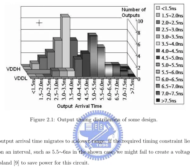
(13) Chapter 2 Clustered Voltage Scaling (CVS) and the Extensions Voltage scaling is one of the most effective techniques in reducing the power consumption of CMOS circuits. However, decreasing VDD leads to increase in circuit delay. In the designs of most microprocessors or ASIC chips, the operating frequency is set by the design specification according to the target market. The timing constraints in chips are in turn set by the operating frequency. Designers need to optimize designs to reduce power consumption within the specified timing constraints. If the supply voltage is reduced while Vth remains constant, the critical-path delay will not meet the timing constraints. CVS is a technology which partially reduces the supply voltage. It utilizes the excess time slack within circuits and then trades the time slack for lower saving.. 2.1. Cluster Voltage Scaling (CVS). Clustered Voltage Scaling, firstly proposed by Usami et al. [10], is a simple and practical technique for low power design. The essence of such technology is based on the utilization of excess timing slack in synchronous circuits. As shown in in Fig. 2.1, the output arrival time of a circuit usually distributes over a range. After lowering down the supply voltage for low power operation, the 3.
(14) Figure 2.1: Output timing distribution of some design.. output arrival time migrates to a slower range. If the required timing constraint lies on an interval, such as 5.5∼6ns in the shown case, we might fail to create a voltage island [9] to save power for this circuit. A possible way to extort power saving is to partially lower down the supply of the cells which have timing slacks, as shown in Fig. 2.2.. Figure 2.2: Cells with different supply voltage [12].. 4.
(15) Figure 2.3: Static Weakly-ON Leakage Current [12].. Apparently, such optimization relies on the inner excess time slack inside circuit blocks. Since most circuits have a critical path and other non-critical paths, we usually have the opportunity to minimize power consumption by virtue of CVS. Note that we can not make a gate supplied by V DDL directly fan out to another gate which is supplied by V DDH . As shown in Fig. 2.3, the sub-threshold current (even worse, a static turn on current) would nullify the efforts done to power saving. We need level converters to shift up signal voltage level so as to drive the succeeding logic gates. Unfortunately, such circuits are relatively large and power consumptive. They form the main overhead of clustered-type multiple-supply-voltage low-power designs when we try to drive V DDH gates with V DDL gates for possibly more power saving. Usami et al. used a kind of specially designed flip-flop with built-in level conversion function (the LCFF) in their CVS technique [10] . To save the overhead induced by level converters, the original CVS paper proposed an algorithm that performs Depth-First-Search (DFS) from each output pins backward toward the input pins to achieve a converter-free solution.. 2.2. Extended Clustered-Voltage-Scaling (ECVS). Usami et al. had proposed two ways to improve CVS in [12]. Firstly, they allow the insertion of level converter. As shown in Fig. 2.4, ECVS algorithm extends CVS 5.
(16) Figure 2.4: Extended CVS (ECVS) [12].. algorithm with a hill-climbing possibility. If the V DDL assignment to cell G3 is feasible (considering the cost of level converter insertion, if necessary) and the total power consumption increment is within a margin, apply it. Secondly, they applied the concept of the stage level of gates, instead of original DFS operation, as the new way to decide the order of V DDL assignments. As shown in Fig. 2.5, they labeled gates and sorted the labeled number as the priority of V DDL assignment.. 2.3. Greedy-ECVS (GECVS). Srivastava et al. had proposed a way to further improve ECVS in [8]. In this paper, they put emphasis on the priority of V DDL assignment. They introduced a concept of sensitivity measurement for further power minimization. They defined the sensitivity of a gate ’x’ as: Sensitivityx =. ∆P ower × sensitivity at gate output ∆Delay. 6.
(17) Figure 2.5: Labeling the level in a logic circuit [12].. where. ∆Power = Change in total power due to move, and ∆Delay = Change in arrival time at gate output due to move. They pointed out a concept that we can exploit the movements according to the best power savings per unit delay penalty. This is a good idea which directly targets at the primitive goal of CVS: trade the excess delay for power saving. Intuitively, this sensitivity measurement seems to give a perfect and non-improvable guideline. In the next Chapter, we provide a better approach to further lowering power consumption in cell-based design.. 7.
(18) 2.4. Problem Formulation. In the following chapters, we formulate our problem as finding the best power saving without violating the timing requirements. The objective is to trade the excess time slacks for most power reduction. Please note that we set up the timing requirements by the Back-roll ratio. The Back-roll ratio means the percentage of increment of the critical path delay. For example, if the Back-roll ratio is 10%, that means the timing requirement is set to 1.1 times the critical path delay. The default value of Back-roll ratio is 0, that is, the timing requirement is equal to the critical path delay.. 8.
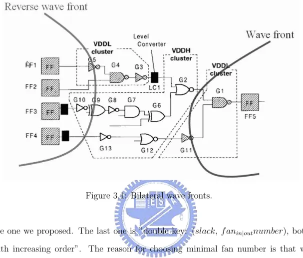
(19) Chapter 3 Bilateral Clustered Voltage Scaling (BCVS) Original CVS does not require any insertion of stand-alone level converters. Therefore, it is a more practical approach than ECVS, especially when the overheads of level converters are still high. As the research and improvement in level converters progress, the overheads of level converters are lowered. We can then utilize more excess slacks by ECVS if the circuit structure and the timing specification allow. Furthermore, GECVS gives a guideline of how to trade slacks for power in an efficient way. In this chapter, we want to show an improved approach to implement Clustered Voltage Scaling.. 3.1. Motivation of BCVS. The term ”bilateral” means that we push our clusters both from the output side and input side. The motivation is that we want to try to push the clusters from both sides alternatively for more possibility to reach the optimal solution. Originally, we try to push both of the wave fronts just n-levels in each step. But the experimental data shows that if n is small, the resulting quality is deteriorated. Therefore, we let n be very large so that the optimality for each wave front is not sacrificed by the action of push of other one. 9.
(20) We have done lots of experiments and observed that such process does little improvement for our benchmark circuits under test. But it true that this process has very good performance for our testing circuits. We ascribe this phenomenon to the difference between circuit structures. For the sake of the adaptability of our algorithm to different circuitry, we reserve this mechanism. So, we start our optimization procedure firstly from the output side and grow the cluster as large as possible if slacks allow. During the wave front traversing on circuit, we mark the best movement sequence of power reduction. As it is finished, we push the other wave front from the input side in the same way”. After one such iteration had been completed, we compare the results. If the solution is better than the previous optimal results, we re-apply the sequence of movement to the marked position and then go on the next iteration.. 3.2. Wave Front Propagation. We utilize a wave front propagator as the engine of our optimizer. As shown in in Fig. 3.1, the wave front starts from the output pins, propagates to the fan-in cells if the timing slacks allow. We also implement a reverse wave front which behaves symmetrically to the ordinary wave front. It starts from the input pins, propagates to the fan-out cells, and automatically includes level converters if necessary. We have designed several testing circuits to test the ability of the wave front and make sure it can find the best solution.. 3.3. Priority Criterion. We have tried three types of propagation priority. The first one is ”single key: ower , with decreasing order”, which stands for the GECVS algorithm. slack* ∆P ∆Delay. The second is ”double key: (slack,. ∆P ower ∆Delay. 10. ), both with increasing order”, which is.
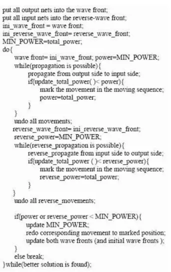
(21) Figure 3.1: Bilateral wave fronts.. the one we proposed. The last one is ”double key: (slack, f anin|out number), both with increasing order”. The reason for choosing minimal fan number is that we want to do least perturbation to the slack distribution of the whole circuit after each V DDL assignment”.. 3.4. BCVS algorithm. The BCV algorithm is shown in Fig. 3.2 . The flow diagram of BCVS is shown in Fig. 3.3 .. 11.
(22) Figure 3.2: BCVS algorithm.. Figure 3.3: BCVS flow diagram.. 12.
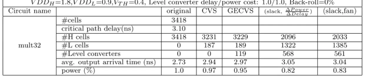
(23) Chapter 4 Experimental Results In this chapter, we show our experimental results and give explanation for the resulting data.. 4.1. Experimental Setup and Modeling. We set our target to find the most power-saving solution on the condition that the maximal input to output arrival time between all the I/O pins remains the same. As the problem formulation in Section 2.4, the program automatically gives timing constraint according to the result of the initial Static Timing Analysis (STA). Then it starts to trade the excess timing slack inside the circuit for best power saving and make sure the timing constraint is still satisfied after each movement. For simplicity, we do not aim to the uphill climbing ability about the timing constraint but set our focus on the strategy to exploit all feasible movement without timing violation, and then mark the most power saving solution we have reached. If the uphill movement support is demanded, we can implement it with special care to the evaluation of timing requirements. To simplify the timing analysis, we set up all gates with the same timing and power parameters. We omitt the information about rise/fall transition time at the I/O pin of each gate so as to focus on the slack/power relation to the wave 13.
(24) Table 4.1: Descriptions of testing circuits Circuit name cla csm add bk mult32. Circuit function 128-bit carry look-ahead adder 128-bit conditional sum adder 128-bit BK adder 32-bit Booth multiplier. of standard cells 1911 1701 1942 3418. propagation inside the circuitry. The reason is our primary goal was to exploit all the feasible movements without timing violation, and secondary mark the best sequence with most power saving. We ignore the portion of power which depends on rise/fall transition time, therefore, the power consumption depends on supply voltage only. In this way, we can emphasize on the relationship between V DDL assignment and resulting reduction on power consumption. We also want to examine the sensitivity criterion proposed by GECVS. So we use UMC 0.18 standard cell library and set different leakage power to each type of cells according to this cell library. Finally, we set the delay/power of level converters to be multiples of unit gate delay/power, respectively. 4.2. Results and Discussions. We use some real designs as our test bench. They are listed in Table 4.1. Then we test them under five types of setup conditions, which are listed in Table 4.2 We have observed that there are two groups of strange data set. First, in Table 4.6, the performance of GECVS seems to be too bad. The reason is that GECVS mixed up the information of timing slack with. ∆P ower ∆Delay. and the key of selection. criterion. So it can not make the right decision that ”the cells with larger timing slack 14.
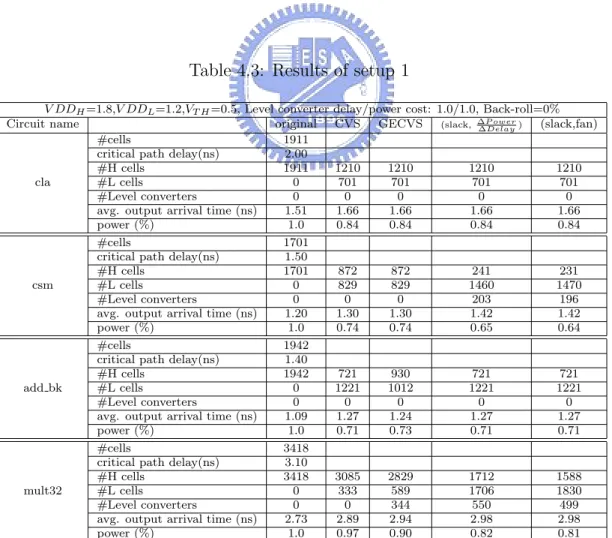
(25) Table 4.2: Setup conditions Setup No. 1 2 3 4 5 6. V DDH 1.8 1.8 1.8 1.8 1.8 1.8. V DDL 1.2 1.2 1.2 0.9 1.2 1.2. VT H 0.5 0.5 0.5 0.4 0.5 0.5. Level converter delay cost 1.0 4.0 0.0 1.0 1.0 1.0. Level converter power cost 1.0 4.0 0.0 1.0 1.0 1.0. Back roll ratio(%) 0 0 0 0 10 20. Table 4.3: Results of setup 1 V DDH =1.8,V DDL =1.2,VT H =0.5, Level converter original Circuit name 1911 #cells 2.00 critical path delay(ns) 1911 #H cells 0 #L cells cla 0 #Level converters 1.51 avg. output arrival time (ns) 1.0 power (%) 1701 #cells 1.50 critical path delay(ns) 1701 #H cells 0 #L cells csm 0 #Level converters 1.20 avg. output arrival time (ns) 1.0 power (%) 1942 #cells 1.40 critical path delay(ns) 1942 #H cells 0 #L cells add bk 0 #Level converters 1.09 avg. output arrival time (ns) 1.0 power (%) 3418 #cells 3.10 critical path delay(ns) 3418 #H cells 0 #L cells mult32 0 #Level converters 2.73 avg. output arrival time (ns) 1.0 power (%). 15. delay/power cost: 1.0/1.0, Back-roll=0% ower ) (slack,fan) CVS GECVS (slack, ∆P ∆Delay 1210 701 0 1.66 0.84. 1210 701 0 1.66 0.84. 1210 701 0 1.66 0.84. 1210 701 0 1.66 0.84. 872 829 0 1.30 0.74. 872 829 0 1.30 0.74. 241 1460 203 1.42 0.65. 231 1470 196 1.42 0.64. 721 1221 0 1.27 0.71. 930 1012 0 1.24 0.73. 721 1221 0 1.27 0.71. 721 1221 0 1.27 0.71. 3085 333 0 2.89 0.97. 2829 589 344 2.94 0.90. 1712 1706 550 2.98 0.82. 1588 1830 499 2.98 0.81.
(26) Table 4.4: Results of setup 2 V DDH =1.8,V DDL =1.2,VT H =0.5, Level converter original Circuit name 1911 #cells 2.00 critical path delay(ns) 1911 #H cells 0 #L cells cla 0 #Level converters 1.51 avg. output arrival time (ns) 1.0 power (%) 1701 #cells 1.50 critical path delay(ns) 1701 #H cells 0 #L cells csm 0 #Level converters 1.20 avg. output arrival time (ns) 1.0 power (%) 1942 #cells 1.40 critical path delay(ns) 1942 #H cells 0 #L cells add bk 0 #Level converters 1.09 avg. output arrival time (ns) 1.0 power (%) 3418 #cells 3.10 critical path delay(ns) 3418 #H cells 0 #L cells mult32 0 #Level converters 2.73 avg. output arrival time (ns) 1.0 power (%). delay/power cost: 4.0/4.0, Back-roll=0% ower ) (slack,fan) CVS GECVS (slack, ∆P ∆Delay 1210 701 0 1.66 0.84. 1210 701 0 1.66 0.84. 1210 701 0 1.66 0.84. 1210 701 0 1.66 0.84. 872 829 0 1.30 0.74. 872 829 0 1.30 0.74. 872 829 0 1.30 0.74. 872 829 0 1.30 0.74. 721 1221 0 1.27 0.71. 930 1012 0 1.24 0.73. 721 1221 0 1.27 0.71. 721 1221 0 1.27 0.71. 3085 333 0 2.89 0.97. 3085 333 0 2.89 0.97. 3085 333 0 2.89 0.97. 3085 333 0 2.89 0.97. Table 4.5: Results of setup 3 V DDH =1.8,V DDL =1.2,VT H =0.5, Level converter original Circuit name 3418 #cells 3.10 critical path delay(ns) 3418 #H cells 0 #L cells mult32 0 #Level converters 2.73 avg. output arrival time (ns) 1.0 power (%). delay/power cost: 0.0/0.0, Back-roll=0% ower ) (slack,fan) CVS GECVS (slack, ∆P ∆Delay 3085 333 0 2.89 0.97. 2307 1110 411 2.92 0.72. 1410 2008 447 2.97 0.63. 1214 2204 463 2.96 0.65. Table 4.6: Results of setup 4 V DDH =1.8,V DDL =0.9,VT H =0.4, Level converter original Circuit name 3418 #cells 3.10 critical path delay(ns) 3418 #H cells 0 #L cells mult32 0 #Level converters 2.73 avg. output arrival time (ns) 1.0 power (%). 16. delay/power cost: 1.0/1.0, Back-roll=0% ower ) (slack,fan) CVS GECVS (slack, ∆P ∆Delay 3231 187 0 2.94 0.97. 3229 189 119 2.97 0.95. 2096 1322 568 3.05 0.82. 2033 1385 561 3.04 0.83.
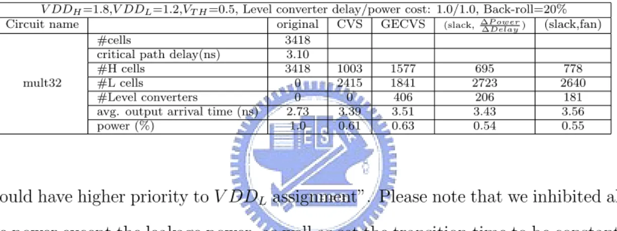
(27) Table 4.7: Results of setup 5 V DDH =1.8,V DDL =1.2,VT H =0.5, Level converter delay/power cost: 1.0/1.0, Back-roll=10% ower ) (slack,fan) original CVS GECVS (slack, ∆P Circuit name ∆Delay 3418 #cells 3.10 critical path delay(ns) 1148 1115 1940 2314 3418 #H cells 2270 2303 1478 1104 0 #L cells mult32 361 350 542 0 0 #Level converters 3.23 3.24 3.26 3.16 2.73 avg. output arrival time (ns) 0.67 0.65 0.77 0.88 1.0 power (%). Table 4.8: Results of setup 6 V DDH =1.8,V DDL =1.2,VT H =0.5, Level converter delay/power cost: 1.0/1.0, Back-roll=20% ower ) (slack,fan) original CVS GECVS (slack, ∆P Circuit name ∆Delay 3418 #cells 3.10 critical path delay(ns) 778 695 1577 1003 3418 #H cells 2640 2723 1841 2415 0 #L cells mult32 181 206 406 0 0 #Level converters 3.56 3.43 3.51 3.39 2.73 avg. output arrival time (ns) 0.55 0.54 0.63 0.61 1.0 power (%). should have higher priority to V DDL assignment”. Please note that we inhibited all the power except the leakage power, as well as set the transition time to be constant. So GECVS had detected a larger. ∆P ower ∆Delay. while the actual delay remains constant.. This is the reason for the unexpected results. Second, in Table 4.5, the (slack,fan) set obtains much more number of V DDL cells than the (slack,. ∆P ower ) ∆Delay. set. But the. final power ratio seems to be inconsistent. The reason is the (slack,fan) criterion can not detect the difference in power saving between cells. The criterion proposed by GECVS multiplies. ∆P ower ∆Delay. with slack, so that the. information of slack is blurred. It can not determine whether the cell has a large slack or a large. ∆P ower . ∆Delay. As we know, the slacks carrie information about the circuit. topology, so we can use it as an observer of topology/timing behavior of the circuit. However, our target is the most power saving rather than the largest slack utilization. That is why we need two keys, one observe the topology and timing, the other measure the location of most power saving.. 17.
(28) In general, if a function α can be a good measurement of the topology/timing information for the propagation algorithm, while our final target is to get the most change in function β, we should use α as the primary key and dβ/dα as the secondary key. That is the reason that we propose slack as the first key and secondary key.. 18. ∆P ower ∆Delay. as the.
(29) Chapter 5 Conclusions and Future Works We have successfully improved Clustered Voltage Scaling technologies by assigning better priority/sensitivity. Through well-defined cost function, we have shown that our priority criterion performs better than the one defined in GECVS (the sensitivity). The short circuit power contributes a large portion of total power consumption. However, to analyze this effect, we need more precise timing analysis to evaluate transition time and its sensitivity. Such a work requires much more efforts, especially if we want to merge it into our algorithms in an efficient way. So our first future work is to try to upgrade our optimizer so that we can perform STA with more practical precision. Our secondary future work is to solve the power scheme problems in an efficient way. And hope that we can integrate CVS and power scheme optimization to obtain better solutions.. 19.
(30) Bibliography [1] Anirban Basu, Sheng-Chih Lin, Vineet Wason, Amit Mehrotra, and Kaustav Banerjee. “Simultaneous Optimization of Supply and Threshold Voltages for Low-Power and High-Performance Circuits in the Leakage Dominant Era”. In Proceedings IEEE/ACM Design Automation Conference, pages 884–887, 2004. [2] Chandrakasan, A.P., S. Sheng, Brodersen, and R.W. “Low power CMOS digital design”. IEEE Journal of Solid-State Circuits, 27(4):473–484, April 1992. [3] Chunhong Chen, Ankur Srivastava, and Majid Sarrafzadeh. “On Gate Level Power Optimization Using Dual-Supply Voltages”. IEEE Transactions on Very Large Scale Integration (VLSI) Systems, 9(5):616–629, October 2001. [4] Srinivas Devadas and Sharad Malik. “A Survey of Optimization Techniques Targeting Low Power VLSI Circuits”. In Proceedings IEEE/ACM Design Automation Conference, pages 242–247, 1995. [5] K. Joe Hass and David F. Cox. “Level Shifting Interfaces for Low Voltage Logic”. In Proceedings NASA Symposium on VLSI Design, pages 3.1.1–3.1.7, 2000. [6] James T. Kao and Anantha P. Chandrakasan. “Dual-Threshold Voltage Techniques for Low-Power Digital Circuits”. IEEE Journal of Solid-State Circuits, 35(7):1009–1018, July 2000.. 20.
(31) [7] Tanay Karnik, James Tschanz Yibin Ye, Liqiong Wei, Steven Burns, Venkatesh Govindarajulu, Vivek De, and Shekhar Borkar. “Total Power Optimization By Simultaneous Dual-Vt Allocation and Device Sizing in High Performance Microprocessor”. In Proceedings IEEE/ACM Design Automation Conference, pages 486–491, 2002. [8] Sarvesh H. Kulkarni, Ashish N. Srivastava, and Dennis Sylvester. “A New Algorithm for Improved VDD Assignment in Low Power Dual VDD Systems”. In Proceedings ACM International Symposium on Low Power Electronics and Design, pages 200–205, 2004. [9] David E. Lackey, Paul S. Zuchowski, Thomas R. Bednar, Scott W. Gould Douglas W. Stout, and John M. Cohn. “Managing Power and Performance for System-on-Chip Designs using Voltage Islands”. In Proceedings IEEE/ACM International Conference on Computer-Aided Design, pages 195–202, 2002. [10] Kimiyoshi Usami and Mark Horowitz. “Clustered Voltage Scaling Technique for Low-Power Design”. In Proceedings ACM International Symposium on Low Power Design, pages 3–8, 1995. [11] Kimiyoshi Usami, Mutsunori Igarashi, Takashi Ishikawa, Masahiro Kanazawa, Masafumi Takahashi, Mototsugu Hamada, Hideho Arakida, Toshihiro Terazawa, and Tadahiro Kuroda.. “Design Methodology of Ultra Low-power. MPEG4 Codec Core Exploiting Voltage Scaling Techniques”. In Proceedings IEEE/ACM Design Automation Conference, pages 483–488, 1998. [12] Kimiyoshi Usami, Mutsunori Igarashi, Fumihiro Minami, Takashi Ishikawa, Masahiro Kanazawa, Makoto Ichida, and Kazutaka Nogami. “Automated LowPower Technique Exploiting Multiple Supply Voltages Applied to a Media Processor”. IEEE Journal of Solid-State Circuits, 33(3):463–472, March 1998.. 21.
(32)
數據
![Figure 2.3: Static Weakly-ON Leakage Current [12].](https://thumb-ap.123doks.com/thumbv2/9libinfo/8638912.193046/15.918.321.573.156.296/figure-static-weakly-on-leakage-current.webp)
![Figure 2.4: Extended CVS (ECVS) [12].](https://thumb-ap.123doks.com/thumbv2/9libinfo/8638912.193046/16.918.148.749.163.558/figure-extended-cvs-ecvs.webp)
![Figure 2.5: Labeling the level in a logic circuit [12].](https://thumb-ap.123doks.com/thumbv2/9libinfo/8638912.193046/17.918.150.741.154.675/figure-labeling-level-logic-circuit.webp)
+7

相關文件
• Examples of items NOT recognised for fee calculation*: staff gathering/ welfare/ meal allowances, expenses related to event celebrations without student participation,
a) Excess charge in a conductor always moves to the surface of the conductor. b) Flux is always perpendicular to the surface. c) If it was not perpendicular, then charges on
In this work, for a locally optimal solution to the NLSDP (2), we prove that under Robinson’s constraint qualification, the nonsingularity of Clarke’s Jacobian of the FB system
CeBIT is the world's largest trade fair showcasing digital IT and CeBIT is the world's largest trade fair showcasing digital IT and5. telecommunications solutions for home and work
Since it is so, what do we cultivate for?People are looking for the ways to improve the mental state, and the courage or wisdom to face the hard moments.. But the ways of improving
• We need to make each barrier coincide with a layer of the binomial tree for better convergence.. • The idea is to choose a Δt such
This paper aims to study three questions (1) whether there is interaction between stock selection and timing, (2) to explore the performance of "timing and stock
From those examples, it indicates that the efflorescence will reoccur after three to six months using the waterproofing membrane painted on the inside of an exterior wall and it
