電信工程學系
博 士 論 文
超寬頻及高整合模組應用之縮小化天線
Miniaturized Antennas for Ultra-Wideband
and High Integration Module Applications
研 究 生:凌菁偉
Ching-Wei Ling
指導教授:鍾世忠 博士
Dr. Shyh-Jong Chung
Miniaturized Antennas for Ultra-Wideband and High
Integration Module Applications
研究生:凌菁偉
Student:
Ching-Wei
Ling
指導教授:鍾世忠 博士 Advisor:
Dr.
Shyh-Jong
Chung
國立交通大學
電信工程學系
博士論文
A Dissertation
Submitted to Department of Communication Engineering
College of Electrical and Computer Engineering
National Chiao Tung University
in Partial Fulfillment of the Requirements
for the Degree of Doctor of Philosophy
in
Communication Engineering
Hsinchu, Taiwan
本論文旨在縮小化天線之研究,包含超寬頻天線以及高整合度模組兩方面的 應用。本研究所提出的天線設計,均具備結構簡單、製作與積體化容易、成本低 廉,以及良好的阻抗匹配與穩定的輻射場型等特性。 首先,就超寬頻應用方面,本論文提出一種具有二次多項式曲線之單極超寬 頻天線設計。利用所提出的二次多項式方程式,並適當地選擇相關變數達成超寬 頻天線的設計。此外,為了達成具有頻帶截止的功能,我們採用並聯LC 電路架 構,藉由調整電路中電感與電容值,能得到適當的截止頻率與截止頻寬。由實驗 量測結果顯示,具有頻帶截止功能之超寬頻天線,在截止頻帶內之平均天線增益 與全頻帶超寬頻天線相比約小 -18 dBi,而截止頻帶外的增益與輻射場型則與全 頻帶超寬頻天線相似。 再者,本論文提出一種架構簡單、小型化單極似之印刷式超寬頻天線設計。 此天線係由一單極天線支段與一類傳輸線支段所組成,訊號由天線饋入端饋入 後,先通過類傳輸線支段後進入單極天線支段。此一類傳輸線支段在不同操作頻 段具有不同的功能,不僅能提供阻抗匹配之外,同時也可成為主要的輻射體,進 而達成超寬頻的特性。 此外,一具有垂直於水平面的強電場且低側高之超寬頻天線設計,也於本論 文中提出與研究。於接地面上內埋兩個L 形狹縫,不僅能提供額外的共振頻率, 更可改善輸入阻抗匹配,進而得到寬頻的天線特性。再者,由於天線饋入端與短 路端之電流方向,在操作頻帶下均相同的緣故,因此本天線與其他一般印刷式天 線相比,在水平切面上具有更強的垂直電流。至於周圍金屬物體對天線特性的影 響,同樣也於本論文中討論,本天線與金屬平面近距離平行擺放時,仍然維持良 好的輻射特性,並且天線高度僅為5mm。 最後,針對高整合模組應用方面,本研究提出一種一體成形並直接製作於電 路屏蔽盒上之小型化系統封裝天線設計,其應用頻段為無線區域網路 IEEE
行相關電路特性的量測之外,更進一步將此整合後的天線與無線區域網卡上的基
頻電路相連接,其量測之 EVM 在操作頻段內均大於-30dB,具備相當良好的特
性。同時也可由系統封裝天線之優異輻射特性,再次證實此設計實際應用於無線
This dissertation is focused on the miniaturized antenna development for ultra-wideband (UWB) and high integration module applications. These antenna designs have the merits of simple in geometry, easy for manufacture and integration, low-cost, and exhibits a good impedance matching in addition to have stable radiation patterns over the bandwidths.
Firstly, for UWB communication applications, a new binomial curved monopole UWB antenna is introduced. In this study, we propose a new edge curve, characterized by the binomial function and properly choose the parameters of the binomial function, for designing UWB antenna. Besides, to achieve the band notch function with a UWB antenna, the concept of the parallel LC circuit is applied. By adjusting the inductor and capacitor values, the suitable notch frequency and bandwidth can be achieved. The average gain is lower than -18 dBi in the stopband, while the patterns and the gains at frequencies other than in the stopband are similar to that of the antenna without the band-notched function.
Secondly, a simple and compact monopole-like printed ultra-wideband antenna is presented. The antenna is composed of a monopole section and a quasi-transmission line section. The input signal from the feed line first passes through the line section then enters the monopole. The quasi-transmission line section provides different functions as the operating frequency changes. It serves not only as an impedance matching circuit but also a main radiator, which leads to the ultra-wideband performance of the antenna.
Thirdly, a low-profile UWB antenna with strong vertically field has been proposed and investigated. Two L-shaped slits are embedded on the ground plane, which provide additional resonances and improve the input impedance matching thus
stronger vertical polarization field as compared to the conventional printed antenna in horizontal plane. Moreover, the metal body’s effect on the antenna performance also analyzed. The proposed antenna maintains good radiation characteristics while a metal plane is placed parallel under the antenna closely. The proposed antenna has a low-profile of 5 mm.
Finally, a miniaturized antenna design, for the high integration module application has been proposed and demonstrated. This on-package planar inverted-F antenna (PIFA) made from a single folded metal plate and fabricate directly on the shielding package for IEEE 802.11b/g WLAN band applications. In this study, the coupling between the antenna and the RF component embedded inside the package is studied. Moreover, an on-package PIFA integrated with a WLAN front-end module (FEM) and a WLAN card containing the baseband/medium access control (MAC) circuitry is successfully implemented. The Error Vector Magnitude (EVM) in the operating band is better than -30 dB, indicating the good performance of the architecture. From the tested result, it seems that the on-package PIFA has good radiation characteristic and thus suitable for the WLAN communication applications. The prototype has a compact size of 15 mm × 20 mm × 3.5 mm.
在博士班的求學過程中,首先要誠摯感謝我的指導教授鍾世忠博士,老師悉 心的教導,使我得以熟知天線相關理論與實務領域的深奧,並不時的與我討論、 修正研究方向,在我遇到瓶頸困難的時候,給予適當的協助,使得這些年獲益匪 淺。並且,老師對於學問的嚴謹以及認真積極的處事態度更是我學習的典範。此 外,也要特別感謝我的碩士班指導教授黃智裕博士,因為老師的栽培提攜,給予 我鼓勵與信心,讓我能順利的進入交通大學就讀博士班,在此也要表示我內心由 衷的感謝之意。至於本論文能得以完成,除感謝兩位恩師之外,亦得感謝陳俊雄 教授、許博文教授、郭仁財教授、張志揚教授、陳富強教授以及林根煌教授,由 於諸位口試委員給我的建議與評論,使得本論文能更加完善而嚴謹。 博士班四年多的日子裡,實驗室裡共同的生活點滴,不論是學術研究的討 論、言不及意的閒聊、出遊玩樂的喜悅、分食食物的瘋狂…等等,都要感謝912 的學長、同學、學弟妹們,也因為有你們的陪伴,讓這四年的研究生活變的絢麗 多彩。在此特別要感謝的是文信、嘉祐、崇育、諭正給予我研究上相當大的幫助, 譚博、侑信、靖凱、智祥不厭其煩的指出我研究上中的缺失,且總能在我迷惑時 為我解惑,以及何博、佩宗、清標、肇堂、明達在學業與研究上的互相砥礪,而 其他四年來實驗室的所有成員們當然也不能忘記,你們的幫助同樣銘感在心。 在此,也要感謝這四年來陪我ㄧ起成長的好姐妹們,珮華、淑君、淳齡、小 龍、芝綺,謝謝你們一直都在我身邊,和我ㄧ起分享生命中的歡笑與淚水,不斷 給我鼓勵與支持,讓我有繼續前進的動力。此外,感謝為我熬夜校稿的又正、連 進與世興,因為你們的協助,讓論文文法錯誤少了許多。同時,更要感謝我摯愛 的雙親,不只默默地支持我,任何時候也都會做我最溫暖而堅強的後盾,讓我能 無後顧之憂的全心研究,進而完成博士班的學業。 最後,謹以此文獻給所有關心我與我關心的人!
摘 要...i
Abstract... iii
致 謝...v
Contents ...vi
List of Tables... viii
List of Figures ...ix
Chapter 1 Introduction ...1
1.1 Motivation ...1
1.2 Literature Survey ...6
1.3 Contributions ...10
1.4 Outline of the Dissertation...12
Chapter 2 Planar Ultra-wideband Antennas...15
2.1 Planar Binomial Curved Monopole Antenna for Ultra-Wideband Communication ...15
2.1.1 Antenna Configuration...16
2.1.2 Parameter Analysis...18
2.1.3 Experiment Results ...20
2.1.4 Summary...22
2.2 Planar Ultra-wideband Antenna with a New Band-Notch Structure...22
2.2.1 Antenna Configuration...23
2.2.2 Antenna Design...24
2.2.3 Experiment Results ...34
2.2.4 Summary...38
Chapter 3 A Simple Monopole-like Printed Ultra-wideband Antenna with a Quasi-Transmission Line Section ...39
3.1 Antenna Configuration ...39
3.2 Resonances of the Antenna...41
3.3 Effect of the Quasi-Transmission Line Section...44
3.4 Parameters Analysis...46
3.5 Experiment Results...52
3.6 Summary...55
Chapter 4 Low-Profile Ultra-Wideband Antenna with Strong Vertical Polarization Field ...56
4.1 Configuration and Design...56
Chapter 5 Analysis and Application of an On-Package Planar Inverted-F Antenna....77
5.1 Configuration and Design...77
5.2 Coupling Between On-Package PIFA and RF Components...85
5.3 Integration of On-Package PIFA and WLAN Front-End Module...89
5.4 Summary...92
Chapter 6 Conclusions and Suggestions for Future Works...93
6.1 Conclusions ...93
6.2 Suggestions for Future Works ...95
References...97
Appendix...104
Vita...105
Table 3.1 The Measured Peak and Average Gains at Four Resonant Frequencies ..54 Table 4.1 The Measured Peak and Average Gains at Three Resonant Frequencies.74 Table 5.1 The Specifications of Each Component in the WLAN Front-end
Figure 1.1 Illustration of the printed antenna on a PCMCIA card inserted inside a laptop PC for WLAN application. ...4 Figure 1.2 HFSS simulated E-field distribution around the laptop PC housing...5 Figure 1.3 Wideband antenna structure. (a) Use the parasitic element, (b) use the
triple feed. ...6 Figure 1.4 Geometry of the typical UWB antenna. ...7 Figure 1.5 Geometry of the typical wide slot UWB antennas with (a) rectangular
feed, (b) circular feed, and (c) fork feed. ...8 Figure 1.6 Geometry of the band notch UWB antenna design. (a) Cut a slot, (b)
insert a slit, (c) embed a quarter-wavelength tuning stub, (d) use the SRR, (e) put a parasitic element, and (f) modify the feed line structure. ...9 Figure 2.1 Geometry of the planar binomial curved monopole antenna. ...16 Figure 2.2 Antenna forms for G = 0 mm with different order N. (a) N = 1, (b) N =
2, (c) N = 3, (d) N = 4, (e) N = 5, (f) N = 6. ...17 Figure 2.3 Simulated return losses for proposed antenna with different order N, w
= 30 mm, A = 20 mm, W = 46 mm, L = 50 mm, and G = 0.45mm...18 Figure 2.4 Simulated return losses for antenna A with different gap width G, w =
30 mm, A = 20 mm, W = 46 mm, L = 50 mm, and N = 4. ...19 Figure 2.5 Simulated current distributions for the proposed antenna with w = 30
mm, A = 20 mm, W = 46 mm, L = 50 mm, G = 0.45 mm, and N = 4. 20 Figure 2.6 Measured and simulated return losses for proposed antenna with w =
30 mm, A = 20 mm, W = 46 mm, L = 50 mm, G = 0.45 mm, and N = 4. ...21 Figure 2.7 Measured x-z plane radiation patterns at (a) 3.1 GHz, (b) 5.0 GHz and
(c) 8.0 GHz for the proposed antenna with w = 30 mm, A = 20 mm, W = 46 mm, L = 50 mm, G = 0.45 mm, and N = 4...21 Figure 2.8 Photograph of the proposed antenna. ...22 Figure 2.9 Geometry of the proposed antenna. W × L = 24 mm × 35 mm, La = 13
mm, g = 0.6 mm, Lg = 9.7, Ws × Ls = 7 mm × 3.7 mm, Wc = 3.6 mm,
We = 3 mm, r = 3 mm. ...24
Figure 2.10 Simulated return losses for the proposed antenna with various patch length La. Ws = Ls = Wc = We = r = 0 mm. Other geometric
parameters are the same as given in Figure 2.9. ...25 Figure 2.11 Simulated return losses for the proposed antenna with various
Figure 2.12 Simulated return losses for the proposed antenna with various gap g. Other geometric parameters are the same as given in Figure 2.9. ...27 Figure 2.13 Simulated return losses for the proposed antenna of various bevel
length Ls with a fixed value of Ws = 7mm. Other geometric
parameters are the same as given in Figure 2.9. ...28 Figure 2.14 Simulated return losses for the proposed antenna of various bevel
width Ws with a fixed value of Ls = 3.7mm. Other geometric
parameters are the same as given in Figure 2.9. ...28 Figure 2.15 Simulated return losses for the proposed antenna of various slot radii
r with a fixed value of We = 3 mm. Other geometric parameters are
the same as given in Figure 2.9...29 Figure 2.16 Simulated return losses for the proposed antenna of various distance
We with a fixed value of r = 3 mm. Other geometric parameters are
the same as given in Figure 2.9...30 Figure 2.17 Simulated 3-D radiation patterns with and without semicircle slots in
the ground plane of the proposed antenna at 9 GHz...31 Figure 2.18 Simulated return losses for the proposed antenna of various axial
ratio (AR), the minor axis is 2.3 mm with a fixed value of Wc = 3.6
mm. Other geometric parameters are the same as given in Figure 2.9...33 Figure 2.19 Simulated and measured return losses of the proposed antenna for
various T-shaped stub width Wc with a fixed value of AR = 2. Other
geometric parameters are the same as given in Figure 2.9. ...33 Figure 2.20 Simulated current distribution of the proposed antenna at 5.5 GHz. ...34 Figure 2.21 Measured radiation patterns at (a) 3 GHz, (b) 5.5 GHz, (c) 6 GHz,
and (d) 9 GHz. (solid line: Eθ dashed line: Eψ) ...36
Figure 2.22 Gains and radiation efficiency of the proposed antenna with
band-notched function. ...37 Figure 2.23 Photograph of the proposed antenna. (a) Full band design and (b)
with band-notch function design...37 Figure 3.1 Geometries of (a) the proposed antenna and (b) a conventional
monopole antenna. ...40 Figure 3.2 Simulated return loss of the proposed antenna with H = 12.4 mm, w =
2 mm, Lt = 4 mm, wt = 1.5 mm, and G = 0.6 mm. The ground size W
× L = 20 mm × 27 mm. ...41 Figure 3.3 Simulated current distributions of the proposed antenna at (a) 3.66, (b)
conventional antenna, and the equivalent circuit. H = 12.4 mm, w = 2 mm, Lt = 4 mm, wt = 1.5 mm, and G = 0.6 mm. The ground size W
× L = 20 mm × 27 mm. ...45 Figure 3.5 Equivalent circuit model of the proposed antenna at lower frequency
range (f < 5 GHz) with series inductance of 1.3 nH and shunt
capacitance of 0.14 pF...45 Figure 3.6 Simulated return losses for the proposed antenna of various length Lt
of the quasi-transmission line section. Other geometric parameters are the same as given in Figure 3.2...47 Figure 3.7 Simulated return losses for the proposed antenna of various width wt
of the quasi-transmission line section. Other geometric parameters are the same as given in Figure 3.2...48 Figure 3.8 Simulated return losses for the proposed antenna of various gap G.
Other geometric parameters are the same as given in Figure 3.2. ...49 Figure 3.9 Simulated return losses for the proposed antenna of various height H
of the monopole antenna. Other geometric parameters are the same as given in Figure 3.2. ...50 Figure 3.10 Simulated return losses for the proposed antenna of various width w
of the monopole antenna. Other geometric parameters are the same as given in Figure 3.2...50 Figure 3.11 Simulated return losses for the proposed antenna of various length L
of the ground plane. Other geometric parameters are the same as given in Figure 3.2. ...51 Figure 3.12 Simulated return losses for the proposed antenna of various ground
width W. Other geometric parameters are the same as given in Figure 3.2...52 Figure 3.13 Measured and simulated return loss of the proposed antenna...53 Figure 3.14 Measured radiation patterns at (a) 3.67 GHz, (b) 4.65 GHz, (c) 6.29
GHz, and (d) 8.35 GHz. (solid line: Etotal ; dashed line: Ephi ; dotted
line: Etheta) ...54
Figure 3.15 Photograph of the proposed antenna. ...54 Figure 4.1 Geometry of the low-profile UWB antenna. (a) 3-D structure, (b) side
view of x-z plane, (c) side view of y-z plane, and (d) top view of x-y plane...58 Figure 4.2 Simulated return loss for the proposed antenna shown in Figure 4.1
with and without slits. wa ×Aa = 25 mm × 17 mm, W × L = 34 mm × 75 mm, w1 ×A1= 9 mm × 3 mm, w2 ×A2= 9.5 mm × 4 mm, w3 × A3
Figure 4.3 Comparison of the simulated return loss for the proposed antenna with different arrangement of the embedded slits. Other geometric
parameters are the same as given in Figure 4.2. ...60 Figure 4.4 The effect on the resonance frequencies with various slit length of
(a)A2and (b)A1. ...61 Figure 4.5 Simulated current distributions of the proposed antenna at (a) 3.19, (b)
3.71, and (c) 4.41GHz...62 Figure 4.6 Simulated return loss for the proposed antenna of various feed
position s. Other geometric parameters are the same as given in
Figure 4.2. ...64 Figure 4.7 Simulated return loss for the proposed antenna of various feed depth d.
Other geometric parameters are the same as given in Figure 4.2. ...64 Figure 4.8 Simulated return loss for the proposed antenna of various short
position. Other geometric parameters are the same as given in Figure 4.2...65 Figure 4.9 Simulated return loss for the proposed antenna of various shorting
strip width ws. Other geometric parameters are the same as given in
Figure 4.2. ...66 Figure 4.10 Simulated return loss for the proposed antenna of various antenna
height h. Other geometric parameters are the same as given in Figure 4.2...67 Figure 4.11 Side view of the low-profile UWB antenna placed parallel under a
metal plane...68 Figure 4.12 Simulated return losses for the proposed antenna above a metal plane
of various distance D. Other geometric parameters are the same as given in Figure 4.2. ...69 Figure 4.13 Simulated return losses for the reference antenna above a metal
plane of various distance D...70 Figure 4.14 Simulated xy-plane radiation patterns without metal plane at (a) 4.41
GHz and with metal plane at (b) 4.45 GHz for the proposed antenna of D = 0.5 cm. (dashed line: Eθ dotted line: Eψ)...71
Figure 4.15 Simulated xy-plane radiation patterns without meta plane at (a) 4.08 GHz and with metal plane at (b) 4.45 GHz for the printed UWB
antenna of D = 0.5 cm. (dashed line: Eθ dotted line: Eψ ) ...72
Figure 4.16 Measured and simulated return losses for proposed antenna with and without a metal plane...73
Figure 4.18 Measured peak gain of the proposed antenna at xy-plane. ...75 Figure 4.19 The photographs of the fabricated antenna. (a) Front view and (b)
back view. ...75 Figure 5.1 Geometry of the on-package PIFA. (a) 3-D structure, (b) side view of
xz-plane, (c) side view of yz-plane...79 Figure 5.2 Return loss of on-package PIFA with various gap widths between the
shorting strip and the feed strip; Aa × wa = 14.5 mm × 15 mm, Ap ×
wp = 15 mm × 20 mm, W × L = 20 mm × 40 mm, h = 1.5 mm, and s =
0 mm. ...80 Figure 5.3 Return loss of on-package PIFA with various shorting strip positions.
Other geometric parameters are the same as given in Figure 5.2. ...81 Figure 5.4 Return loss of on-package PIFA with various shielding package sizes.
Other geometric parameters are the same as given in Figure 5.2. ...82 Figure 5.5 Return loss of on-package PIFA with various shielding package
heights. Other geometric parameters are the same as given in Figure 5.2...83 Figure 5.6 Return loss of on-package PIFA with various ground lengths. Other
geometric parameters are the same as given in Figure 5.2. ...83 Figure 5.7 Manufacture procedure of on-package PIFA...84 Figure 5.8 Measured and simulated return loss of on-package PIFA. Aa × wa =
14.5 mm × 15 mm, Ap × wp = 15 mm × 20 mm, W × L = 20 mm × 40
mm, h = 1.5 mm, g = 1 mm, and s = 0 mm. ...85 Figure 5.9 Illustration of BPF locations. Ap × wp = 15 mm × 20 mm ...86
Figure 5.10 Simulation results of the scattering parameters with BPF at various locations. (a) Return loss (-S11) and insertion loss (-S21) of the BPF, (b) isolation (-S13) between ports 1 and 3, and (c) isolation (-S23) between ports 2 and 3. The geometrical parameters are the same as given in Figure 5.8. ...88 Figure 5.11 Return loss of the on-package PIFA with BPF integrated. The
geometric parameters are the same as given in Figure 5.8. ...88 Figure 5.12 Radiation patterns of the on-package PIFA with and without BPF at
2.45GHz for (a) xz- plane, (b) yz-plane, and (c) xy-plane. The
geometric parameters are the same as given in Figure 5.8. ...89 Figure 5.13 Block diagram of on-package PIFA integrated with WLAN front-end
module and WLAN card...90 Figure 5.14 Test results of the EVM and spectrum masks at (a) 2.412 GHz, (b)
Chapter 1 Introduction
Nowadays, with the rapid development of the wireless communications, mobile communication devices become more compact size and light weight. Due to the size reduction requirement, the antenna design trend to miniaturization and high integration module application for the space restriction. Hence, this dissertation focuses on the miniaturized antenna development for ultra-wideband (UWB) and high integration module applications. This chapter firstly describes the motivation of the research and discusses the related antenna design literatures. The contributions of this dissertation are presented next. Lastly, the outline of the following chapters is provided.
1.1 Motivation
The antenna is a key component for all wireless communication systems. With the rapid development of the wireless communications, many systems now operate in two or more frequency bands, requiring dual-band or multi-band functioned antennas. These systems include GSM (880-960 MHz), DCS (1700-1880 MHz), UMTS (1920-2170 MHz), WiBro (2300-2390 MHz), WLAN (2400-2483 MHz, 5150-5825 MHz), and combinations of them. The conventional antennas which are specified for a rather narrow bandwidth are insufficient for use. The ultra-wideband (UWB) antennas, which are usually designed to use single antenna structure with broadband operation, become attractive for the benefits of simpler structure than multi-band designs with several narrow-banded elements. Here, the UWB antennas mean those with a relative impedance bandwidth larger than 25% [1]. Besides, according to the regulations released by Federal Communications Commission (FCC) in February 2002, one of the
UWB systems has been allocated to the frequency band of 3.1 to 10.6 GHz [2] for the merits of high transmission rate, high capacity, and low power consumption. Thus, there is a growing demand on antenna design for a simple and compact structure with wideband operation, both for the integration usage of multi-mode multi-frequency systems and for an UWB system.
The UWB systems can be divided into two categories: Direct Sequence UWB (DS-UWB) and Multi-Band Orthogonal Frequency Division Multiplexing (MB-OFDM). The DS-UWB proposed that UWB system supports operation in two different bands: one band nominally occupying the spectrum from 3.1 to 4.85 GHz (the low band), and the second band nominally occupying the spectrum from 6.2 to 9.7 GHz (the high band). By the MB-OFDM format in 802.15.3a, the interval between 3.1 and 10.6 GHz is divided into 13 sub-intervals. Each sub-interval corresponds to one band of the MB-OFDM, with the width of 528 MHz. The MB-OFDM proposal foresees two different operating modes: a mandatory Mode 1 and an optional Mode 2. Mode 1 uses three operating bands: Band 1 (3.168-3.696 GHz), Band 2 (3.696-4.224 GHz), and Band 3 (4.224-4.752 GHz). Mode 2 uses seven bands: Band 1, 2, 3 (as in Mode 1), Band 6 (6.072-6.60 GHz), Band 7 (6.60-7.128 GHz), Band 8 (7.128-7.656 GHz), and Band 9 (7.656-8.184 GHz). The four unmentioned bands, i.e. Bands 10-13 (8.184-10.296 GHz), have been reserved for future use [3]-[4]. Therefore, there is a sparked attention on UWB antenna technology in the industry and academia for commercial use. And more and more researchers get involve in developing UWB antennas which satisfy the regulations. Besides, using the lower band operation can provide long-distance transmission and non-line of sight (NLOS) propagation is used for deliver broadband data to a wide range of users. Hence, much research is focus on the DS low band design.
However, despite the approval of the FCC for UWB to operate over 3.1 to 10.6 GHz, it may be necessary to notch-out portions of the band in order to avoid interference with the existing wireless networking technologies such as IEEE 802.11a in the U.S. (5.15-5.35 GHz, 5.725-5.825 GHz) and HIPERLAN/2 in Europe (5.15-5.35 GHz, 5.47-5.725 GHz). This is due to the fact that UWB transmitters should not cause any electromagnetic interference to nearby communication system like the Wireless Local Area Network (WLAN) applications. Hence, UWB antennas design with notched characteristics in the WLAN frequency band are required.
Besides, the other miniaturized antenna design for WLAN System-on-Package (SOP) application is investigated. WLAN has been one of the most important applications of wireless communication technology in recent years. The WLAN standards have been developed by the Institute of Electrical and Electronics Engineers (IEEE) and the 802.11 standard is a family of specifications for WLAN technology. For instance, WLAN in the 2.4 GHz band (2.40-2.4835 GHz) of IEEE 802.11b/g has been developed widely and rapidly applied by using wireless communication terminals, such as desktop computers, laptop computers, mobile phones, personal digital assistants (PDAs), etc. Nowadays, SOP technology is one solution for establishing future wireless transceiver modules that can provide flexibility by integrating all functional blocks using the multi-layer process and novel interconnection methods. To enhance the function of SOP for wireless communications, it has become very attractive to develop the SOP which is efficiently to integrate an antenna with a module. Therefore, the antenna in SOP is a significant subject for investigation and thus our motivation is to design the antenna for high integration module application.
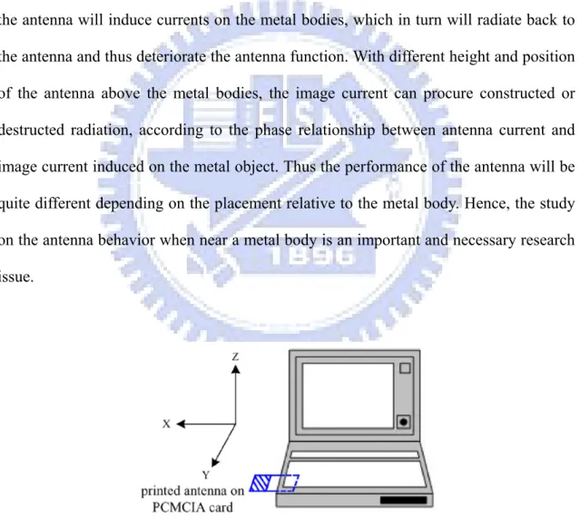
Furthermore, the antenna performance is affected by the operating environment, especially when metal bodies are nearby the antenna. In the practical using environment, the antenna might be placed parallel above a metal body such as metal-like table, PC
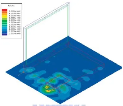
case or placed near the LCD screen edges, inserted inside a laptop, and so on. Figure 1.1 shows a practical environment of a PCMCIA (Personal Computer Memory Card International Association) card (within a PIFA or monopole antenna) inserts inside a laptop. The simulated E-field distribution around the laptop is shown in Figure 1.2. In this case, when the antenna is operating, fringing fields are expected to be present externally; thus, coupling between the antenna and the nearby associated elements (e.g., a metal-like table under the antenna) will occur. This possible coupling will then cause degradation effects on the antenna performances. Moreover, the EM wave radiated from the antenna will induce currents on the metal bodies, which in turn will radiate back to the antenna and thus deteriorate the antenna function. With different height and position of the antenna above the metal bodies, the image current can procure constructed or destructed radiation, according to the phase relationship between antenna current and image current induced on the metal object. Thus the performance of the antenna will be quite different depending on the placement relative to the metal body. Hence, the study on the antenna behavior when near a metal body is an important and necessary research issue.
Figure 1.1 Illustration of the printed antenna on a PCMCIA card inserted inside a laptop PC for WLAN application.
Figure 1.2 HFSS simulated E-field distribution around the laptop PC housing.
Moreover, the typical transmitting antenna type of the Access Point (AP) antenna might have a monopole antenna structure, which has a strong vertical polarization field. If the receiving antenna is of printed type and has strong horizontal polarization field. That will cause deterioration in quality communication while there’s different polarization between the transmitter and receiver antenna. Although increasing the antenna height can improve the vertical polarization field but the height is restricted to the practical use environment and the device size. Hence, designing a low-profile UWB antenna with high vertical polarization field is also an investigation necessary.
In summary, a series of miniaturized antenna designs were proposed. For the UWB communication applications, there are four antenna designs. First of all, an internal UWB antenna design for PCMCIA card is presented. Then, a miniature UWB antenna with small size for external applications is also introduced. Finally, a simple structure and a low-profile UWB antenna designs were proposed. In addition, another miniaturized antenna design for the high integration module applications, and an on-package PIFA fabricate directly on the shielding package which can further reduce the device size, had been investigated in this dissertation.
1.2 Literature Survey
According to there is a growing demand on antenna design for a brief structure with wideband operation. There are many researches in the open literature related to achieving the wideband performance. In [5]-[8], using parasitic elements as shown in Figure 1.3 (a), for providing additional current paths, can create more resonant frequencies adjacent to the center one and thus get the wideband operation. Modifying the shape of the feed line is another method for enhancing the bandwidth. It was demonstrated that, applying double or triple feeds to the main antenna structure (as Figure 1.3 (b)) can generate a pure and intense current distribution, leading to the improvements in the polarization properties and impedance bandwidth [9]-[12].
(a) (b)
Figure 1.3 Wideband antenna structure. (a) Use the parasitic element, (b) use the triple feed.
Besides, the UWB antennas proposed in the open literature mainly focus on the monopole and slot antenna. The wideband planar monopole antenna is one of UWB antennas that have attracted a lot of attention because it is simple in geometry, easy for manufacture and integration, and low-cost, and exhibits not only a good impedance matching but also stable radiation patterns over the bandwidths. There are many related studies to the type of antenna having been available in the open literature and most researches focus on the planar design antenna such as half-disc [13]-[14], circular [15]-[17], elliptical [18], triangle [19]-[21], rectangular [22]-[25], bow-tie [26]-[28],
hexagonal [29]-[30], and others with smooth edges [31]-[35], which provide the possible shapes of antennas suitable for UWB application. Most of them were designed with printed “fat” monopole structure to achieve UWB performance. There is usually a small gap between the fat monopole and the ground plane edge as shown in Figure 1.4, which is an important factor for impedance matching, especially in the high frequency range. For these antennas, in the lower operation frequency band, the current is mainly distributed over the monopole and the nearby ground plane edge, which is similar to the current of a resonant monopole. In the higher frequency band, the current is distributed around the gap, therefore, acting like a slot antenna. Due to these appropriate current paths across the full band provided by the antenna structure, the wideband operation is thus achieved.
gap gap gap gap gap gap
Figure 1.4 Geometry of the typical UWB antenna.
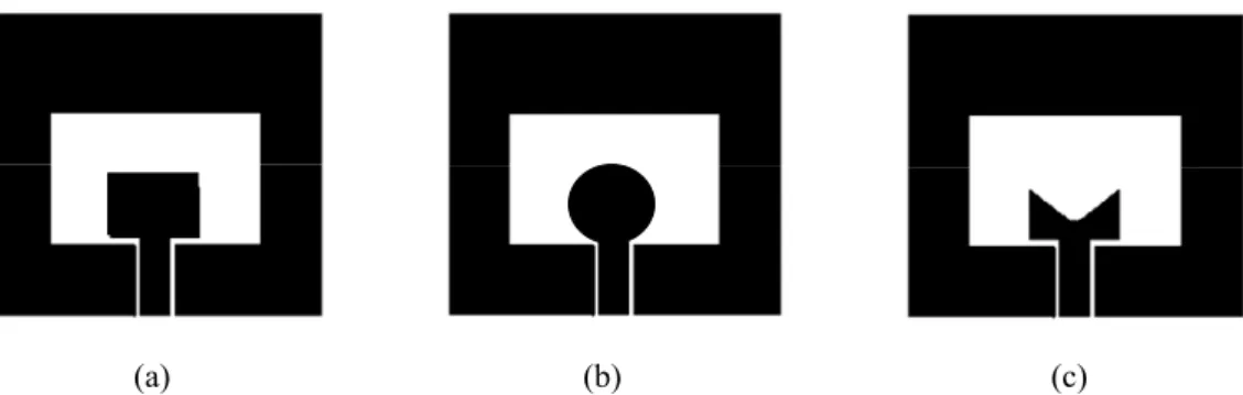
The other one, printed wide slot antennas has an attractive property of providing a wide operating bandwidth, especially for those having a modified tuning stub, such as the fork-like stub [36]-[39], the rectangular stub [40]-[41], and the circular stub [42] inside the wide slot as shown in Figure 1.5. Moreover, there is some research results related to using the ceramic material or Low Temperature Co-fired Ceramic (LTCC) technology, according to that its high dielectric constant material reduces the antenna size and achieves the UWB applications [43]-[45].
(a) (b) (c)
Figure 1.5 Geometry of the typical wide slot UWB antennas with (a) rectangular feed, (b) circular feed, and (c) fork feed.
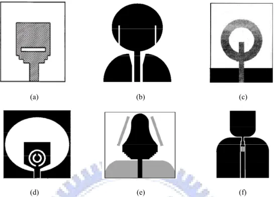
The frequency range for UWB systems approved by the FCC is between 3.1 GHz and 10.6 GHz. It might cause interference with the existing wireless communication systems, for example, the WLAN operating in 5.15-5.85 GHz. Therefore, the UWB antenna with a band-notched characteristic is required. To obtain the band-notched function, there are various methods to achieve it. The conventional methods are cutting a slot (i.e., U-shaped, V-shaped, arc-shaped, and a pie-shaped slot) on the patch [46]-[54], inserting a slit on the patch [55]-[57], embedding a quarter-wavelength tuning stub within a large slot on the patch [58], or using the split ring resonator (SRR) structure on the patch [59]-[60]. Another way is putting parasitic elements near the printed monopole as filters to reject the limited band [61]-[63] or introducing a parasitic open-circuit element, rather than modifying the structure of the antenna’s tuning stub [64]. Changing the feed structure is also a method to achieve the band-notched response such as using the lumped and distributed inductors and capacitors integrated on the top side of the substrate in front of the feed port [65] and inserting two quarter-wavelength tuning stubs or a resonance cell into the proposed feeding [66]-[67]. As mentioned above, at the notch frequency, the current mainly concentrates over the area of the cutting slot, the adding stub and parasitic element, thus, achieving the band notch function.
(a) (b) (c)
(d) (e) (f)
Figure 1.6 Geometry of the band notch UWB antenna design. (a) Cut a slot, (b) insert a slit, (c) embed a quarter-wavelength tuning stub, (d) use the SRR, (e) put a parasitic element, and (f) modify the feed line structure.
As regards the miniaturized antenna design for WLAN application, recently many conventional antennas have been successfully designed for WLAN applications, such as monopole antennas, PIFAs, patch antennas, and dielectric resonator antennas (DRA) [71]-[77]. For the kinds of the printed monopole antenna, the antenna is usually directly excited by a 50Ω microstrip line printed on the same (upper) side of the dielectric substrate [71]-[73]. This kind of internal antenna mainly uses the system ground plane as the antenna’s ground. The system ground-plane dimensions, to some extent, can strongly affect the antenna impedance bandwidth. And the other kind of DRA is attracted the attention of antenna researchers because of its wide impedance bandwidth and flexible coupling schemes [74]. Another kind of antenna design is PIFA that provides several merits of compact size, light weight and low cost [75]-[77]. For establishing future wireless transceiver modules provide flexibility by integrating all functional blocks using the multi-layer process and novel interconnection methods, SOP
technology is one solution. Many single-chip wireless transceivers have been designed, such as those fabricated in 0.25 μm at 1.8 GHz for DCS-1800 applications and at 2.45 GHz for Bluetooth applications [78]. To enhance the function of SOP for wireless communications, it has become very attractive to develop the SOP which integrates an antenna with a module efficiently. In the case that the embedded antennas are integrated with the low temperature co-fired ceramic (LTCC) package, semiconductor substrates, or the ceramic ball grid array package (CBGA), interferences between the antenna and the RF blocks may happen in highly integrated modules [79]-[85]. Usually the patch antenna is employed and stacked on the top above the circuit within the package. The configuration leads to an increase in the overall height of the package and results in narrow-band operation as well. In addition, due to the use of high permittivity dielectric material, the radiation efficiency of the antenna is also limited.
Besides, the antenna performance is affected by the operating environment, especially when metal bodies are nearby the antenna. The EM wave radiated from the antenna will induce currents on the metal bodies, which in turn will radiate back to the antenna and thus deteriorate the antenna function. This possible coupling will then cause degradation effects on the antenna performances. But, there are only few references concerned to the operating environment affecting the antenna characteristics, especially when metal bodies are nearby or under the antenna [68]-[70].
1.3 Contributions
A series of miniaturized antenna designs for UWB and high integration module applications have been established in this dissertation.
First, for the UWB application, although the typical shapes of the UWB monopole antenna include a half-disc, a circle, an ellipse, a rectangle, and others with smooth
edges are published in the open literature as described above. But there are only few references concerned to the edge curve affecting the antenna characteristics. In this dissertation, we present a new method to construct the edge curve of the antenna and analyze parametric effects on the impedance bandwidth. Formulating the curves of the antenna edge by a binomial function, the impedance bandwidths of the proposed antenna can significantly be improved if the parameters of the binomial function are properly selected.
To obtain the band-notched function in the UWB antenna application, then, different approach of the continental design, the concept of the parallel LC circuit is applied. At the resonant frequency, the parallel LC circuit will cause high input impedance that leads to the desired high attenuation and impedance mismatching near the notch frequency. Hence, a pair of T-shaped stubs is embedded inside an elliptical slot cut in the radiation patch to form the parallel LC circuit. The elliptical slot and the T-shaped stubs are equivalent to an inductor and a capacitor, respectively. By adjusting the inductor and capacitor values, the suitable notch frequency and bandwidth can be achieved.
Beside, a new antenna configuration which is different from the printed fat monopoles is proposed for the ultra-wideband operation. The structure is quite simple, containing a conventional printed thin-wire monopole, in addition to a quasi-transmission line section. The input signal from the feed line first passes through the quasi-transmission line section then enters the monopole. The quasi-transmission line section provides impedance matching or antenna radiation at different frequency bands. By properly designing the parameters of this quasi-transmission line section, several current resonances with continuous frequencies can happen in the antenna structure, which thus makes the whole antenna possess wideband performance.
Moreover, in the practical environment, there will cause deteriorate quality of communication while the different polarization propagation between the transmitter and receiver antenna. Hence, in this study, a low-profile DS-UWB antenna with strong vertical polarization field is proposed. According to embedded two L-shaped slits on the ground plane, which provide additional resonances and improve the input impedance matching thus wideband performance can be obtained. Besides, because of the loop structure, the current direction on the feed and the shorting strip are the same, hence, the proposed antenna has stronger vertical polarization field as compared to the conventional printed antenna in the horizontal plane and then maintains good radiation characteristics even while a metal plane is placed parallel under the antenna closely. The antenna has a low profile of 5 mm.
Finally, for high integration module application, an on-package PIFA, consisting of a single folded metal plate for WLAN applications, is proposed. Fabricating an antenna directly on the package has the advantage of reducing feeder loss and the overall size of the circuitry. The shielding package can perform as part of the ground plane and block to eliminate the undesired coupling with nearby RF components and the coupling effect between the on-package PIFA and the RF components in the shielding package is examined. The antenna performance is rarely changed and the isolation between the antenna and the RF components can be maximized by appropriately locating the components in the package. Moreover, an on-package PIFA integrated with a WLAN front-end module and a WLAN card was successfully implemented. The prototype has a compact size of 15 mm × 20 mm × 3.5 mm.
1.4 Outline of the Dissertation
antennas design, and at first, a binomial curved monopole antenna is introduced. We propose a new edge curve characterized by the binomial function, for designing UWB antenna. The effect on the impedance bandwidth through the change with the different order of the binomial function and the gap width between the antenna and ground plane has been investigated and analyzed. Then, a novel planar UWB antenna with band-notched function is proposed. The concept of the parallel LC circuit is applied. The notched band, covering the 5-GHz WiFi band, is achieved by an equivalent parallel LC circuit formed by two T-shaped stubs inside an ellipse slot cut in the radiation patch. The elliptical slot and the T-shaped stubs are equivalent to an inductor and a capacitor, respectively. By adjusting the inductor and capacitor values, the suitable notch frequency and bandwidth can be achieved.
In Chapter 3, a simple and compact monopole-like printed ultra-wideband antenna is presented. The antenna is composed of a monopole section and a quasi-transmission line section. The input signal from the feed line first passes through the line section then enters the monopole. The resonance mechanisms of the proposed ultra-wideband antenna are firstly described. Four antenna resonances with different resonant conditions are examined. The effect of the quasi-transmission line section on the antenna performance is then investigated. Moreover, an equivalent model is proposed to explain the behavior of the line section in the lower frequency band. The geometry parameter study on the impedance bandwidth is done next, followed by the presentation of measured return loss and radiation patterns.
In Chapter 4, a low-profile ultra-wide band antenna with strong vertical polarization field is proposed. The antenna design, including the embedded L-shaped slits mechanisms of the proposed UWB antenna and the simulated current distributions of the proposed antenna, is first described. Besides, in the practical using environment, the performance of the antenna will be quite different depending on the placement relative
to the metal bodies. Hence, the effect on the antenna performance on the metal object will be investigated and a conventional printed UWB antenna is also simulated for comparison. Lastly, the measured return loss and radiation patterns of the proposed antenna are presented.
In Chapter 5, an on-package PIFA made from a single folded metal plate for IEEE 802.11b/g WLAN band applications has been proposed and demonstrated. This antenna is fabricating directly on the shielding package. First, to demonstrate the on-package antenna, several design parameters, such as the package dimensions and ground size, have been analyzed in detail. Secondly, the coupling between the antenna and the RF component embedded inside the package is studied. Next, an on-package PIFA integrated with a WLAN front-end module and a WLAN card was successfully implemented. Finally, the antenna embedded front-end module (AFEM) is first built and measured.
Finally, Chapter 6 concludes the overall dissertation and also provides suggestions for the future works.
Chapter 2
Planar Ultra-wideband Antennas
In this chapter, two planar UWB antennas design are presented. Firstly, by introducing the binomial function for characterized the edge curve of the antenna. Through the change with the different order of the binomial function and the gap width between the antenna and ground plane, the UWB (3.1-10.6 GHz) antenna can be achieved. Secondly, in order to obtain the band-notched function in the UWB antenna application, then, the concept of the parallel LC circuit is applied and proposed. By properly adjust the inductor and capacitor values, the notched band, covering the 5 GHz WiFi band, is obtained.
2.1 Planar Binomial Curved Monopole Antenna for Ultra-Wideband
Communication
The curve of a planar antenna edge is an important parameter which affects the antenna performances. As mentioned in Chapter 1, there are many related studies to the type of antenna having been available in the open literature and most researches focus on the planar design antenna such as half-disc [13]-[14], circular [15]-[17], elliptical [18], triangle [19]-[21], rectangular [22]-[25], bow-tie [26]-[28], hexagonal [29]-[30], and others with smooth edges [31]-[35], which provide the possible shapes of antennas suitable for UWB application.
In this section, we propose a new edge curve, characterized by the binomial function, for designing ultra-wideband (UWB) antenna. The effect on the impedance bandwidth through the change with the different order of the binomial function and the gap width between the antenna and ground plane has been investigated and analyzed. The measurement result shows a good agreement with the simulation. Besides, the radiation patterns are omnidirectional in the H plane across the operating bandwidths.
2.1.1 Antenna Configuration
Figure 2.1 illustrates the geometry of the investigated antenna. This antenna is printed on a FR4 microwave substrate with the thickness of 0.8mm and the dielectric constant of 4.4. The areas of the monopole antenna and the ground plane are denoted as
w × A and W × L, respectively. A 50 Ω microstrip feed line of 1.5 mm width is
etched on the same side of the monopole. The gap width between the monopole antenna and the ground plane is G. Hence, the whole substrate size of the antenna is W × (A+ G+ L). W L G x y w E (w/2, ) A A W L G x y w E (w/2, ) A A
Figure 2.1 Geometry of the planar binomial curved monopole antenna.
The curve of a planar antenna edge is an important parameter which affects the antenna characteristics. The parametric effects on the impedance bandwidth of the proposed antenna are analyzed by utilizing a binomial function. The function includes parameters of the length A and width w of the antenna, the gap width G between the antenna and the ground plane, and the order N of the binomial function, which is
expressed as follows: 2 0 , 2 ) ( x w w x G x f y N ≤ ≤ ⎟ ⎟ ⎠ ⎞ ⎜ ⎜ ⎝ ⎛ + = = A (2.1)
where (x, y) is the coordinate of the curved boundary. In this study, the vertex point E (w/2,A) is fixed, with w = 30 mm and A = 20 mm. By selecting the different order N and the gap width G, we can obtain the half shape of the antenna and then mirror along with y axis to obtain the whole antenna configuration.
The antenna shape is like a triangle with N = 1 as shown in Figure 2.2(a). When N approaches infinite, the shape of the antenna looks like a rectangle. Figure 2.2 shows the antenna configurations for G = 0 mm with different order N from 1 to 6.
(a) (b) (c)
(d) (e) (f)
Figure 2.2 Antenna forms for G = 0 mm with different order N. (a) N = 1, (b) N = 2, (c) N = 3, (d) N = 4, (e) N = 5, (f) N = 6.
2.1.2 Parameter Analysis
In this section, the effects with respect to parameters N and G of the binomial function on impedance bandwidth are discussed. The simulation results shown below are tackled by using the commercial 3-D full-wave electromagnetic (EM) simulation software package, Ansoft High Frequency Structure Simulator (HFSS) [90].
Figure 2.3 shows the simulated return losses of the proposed antenna for G = 0.45 mm with different binomial order N. The relationship between the order N and return loss is not obvious, but by selecting the order N properly, it can be observed that the proposed antenna can cover the frequency band 2.65-10.4 GHz for the case of N = 4.
2 3 4 5 6 7 8 9 10 11 Frequency (GHz) 40 30 20 10 0 R e tu rn L o s s (d B ) N = 1 N = 2 N = 3 N = 4 N = 5 N = 6 2 3 4 5 6 7 8 9 10 11 Frequency (GHz) 40 30 20 10 0 R e tu rn L o s s (d B ) N = 1 N = 2 N = 3 N = 4 N = 5 N = 6
Figure 2.3 Simulated return losses for proposed antenna with different order N, w = 30 mm, A = 20 mm,
W = 46 mm, L = 50 mm, and G = 0.45mm.
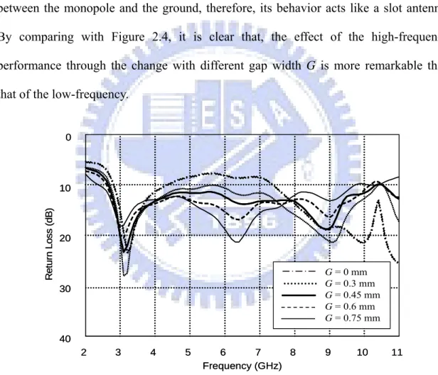
Furthermore, it should also be noted that the gap width G between the antenna and the ground plane has important effect on the impedance bandwidth of the proposed
design can further be improved by selecting G. The bandwidth increases if G > 0.3 mm. In particular, the widest 10 dB return-loss bandwidth, from 2.7 GHz to more than 11 GHz, occurs when G = 0.45 mm and N = 4.
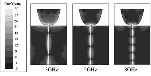
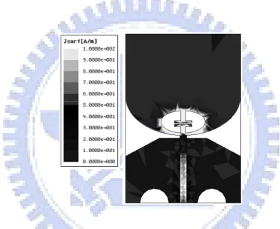
The simulated current distributions for the proposed antenna at the frequencies 3, 5, and 8 GHz are shown in Figure 2.5. At 3 GHz, the current is mainly distributed over the monopole and the upper edge of ground plane, which is similar to the current of a printed resonant monopole. At 8 GHz, the current is mainly distributed around the gap between the monopole and the ground, therefore, its behavior acts like a slot antenna. By comparing with Figure 2.4, it is clear that, the effect of the high-frequency performance through the change with different gap width G is more remarkable than that of the low-frequency.
2 3 4 5 6 7 8 9 10 11 Frequency (GHz) 40 30 20 10 0 R e turn L o ss (d B ) G = 0 mm G = 0.3 mm G = 0.45 mm G = 0.6 mm G = 0.75 mm 2 3 4 5 6 7 8 9 10 11 Frequency (GHz) 40 30 20 10 0 R e turn L o ss (d B ) G = 0 mm G = 0.3 mm G = 0.45 mm G = 0.6 mm G = 0.75 mm
Figure 2.4 Simulated return losses for antenna A with different gap width G, w = 30 mm, A = 20 mm, W
3GHz 5GHz 8GHz 30 27 24 21 18 15 12 9 6 3 0 Jsurf (A/m) 3GHz 5GHz 8GHz 30 27 24 21 18 15 12 9 6 3 0 30 27 24 21 18 15 12 9 6 3 0 Jsurf (A/m)
Figure 2.5 Simulated current distributions for the proposed antenna with w = 30 mm, A = 20 mm, W = 46 mm, L = 50 mm, G = 0.45 mm, and N = 4.
2.1.3 Experiment Results
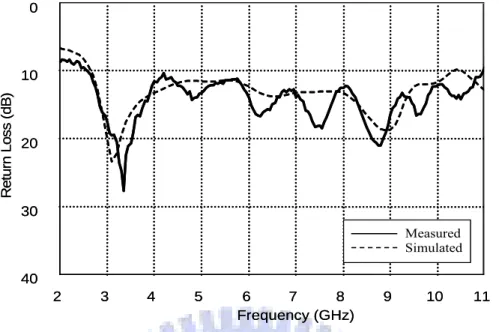
Figure 2.6 shows the measured return loss of the proposed antenna for N = 4 and G = 0.45 mm. The simulation results are also shown for comparison. A good agreement between the measurement and the simulation results is obtained. The measured impedance bandwidth, determined by a 10 dB return loss, is from 2.59 to 10.97 GHz.
The measured radiation patterns of the proposed antenna at the frequencies 3.1, 5.0, and 8.0 GHz in x-z plane are shown in Figure 2.7(a), (b), and (c), respectively. The radiation pattern is omnidirectional and quite stable over the whole frequency band. The measured peak (average) gains for the frequencies of 3.1, 5.0, and 8.0 GHz are, respectively, -0.88 dBi (-3.65 dBi), -2.36 dBi (-4.51 dBi), and 1.54 dBi (-2.1 dBi). Figure 2.8 shows the photograph of the finished antenna.
2 3 4 5 6 7 8 9 10 11 Frequency (GHz) 40 30 20 10 0 R e tu rn L o ss (d B ) Measured Simulated 2 3 4 5 6 7 8 9 10 11 Frequency (GHz) 40 30 20 10 0 R e tu rn L o ss (d B ) Measured Simulated
Figure 2.6 Measured and simulated return losses for proposed antenna with w = 30 mm, A = 20 mm, W
= 46 mm, L = 50 mm, G = 0.45 mm, and N = 4.
(a) (b)
(c)
Figure 2.7 Measured x-z plane radiation patterns at (a) 3.1 GHz, (b) 5.0 GHz and (c) 8.0 GHz for the proposed antenna with w = 30 mm, A = 20 mm, W = 46 mm, L = 50 mm, G = 0.45 mm, and N = 4.
y x z E-total E-phi E-theta E-total E-phi E-theta
Figure 2.8 Photograph of the proposed antenna.
2.1.4 Summary
The planar binomial curved monopole antenna has been proposed and investigated. The antenna has a simple structure and can be designed by utilizing only few parameters. The experiment results show that the impedance bandwidth of the proposed antenna can significantly be improved by selecting the suitable binomial order N and the gap width G. Also show that a wide impedance bandwidth has been obtained, which makes the proposed antenna suitable for UWB (3.1-10.6 GHz) applications. A stable omnidirectional radiation pattern was also obtained for the whole impedance bandwidth.
2.2 Planar Ultra-wideband Antenna with a New Band-Notch
Structure
This section proposes a novel planar UWB antenna with band-notched function. The antenna consists of a radiation patch that has an arc-shaped edge and a partially modified ground plane. The antenna that makes it different from the traditional monopole antenna is the modification in the shape of ground plane, including two bevel slots on the upper edge and two semicircle slots on the bottom edge of the ground plane. These slots improve the input impedance bandwidth and the high frequency radiation
performance. With this design, the return loss is lower than 10 dB in 3.1-10.6 GHz frequency range and the radiation pattern is highly similar to the monopole antenna. By embedding a pair of T-shaped stubs inside an elliptical slot cut in the radiation patch, a notch around 5.5 GHz WLAN band is obtained. The average gain is lower than -18 dBi in the stopband, while the patterns and the gains at frequencies other than in the stopband are similar to that of the antenna without the band-notched function.
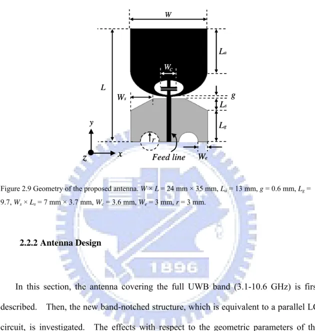
2.2.1 Antenna Configuration
Figure 2.9 shows the geometry of the proposed antenna. It consists of a radiation patch with an arc-shaped edge and a partially modified ground plane with two bevels to achieve a broad bandwidth. The arc-shaped edge of the radiation patch is a half-ellipse with the major axis of 8 mm and the axial ratio of 1.5. The lengths and width of the straight-edges of the radiation patch are La and W, respectively. The bevels with
dimensions of Ws × Ls are placed on the upper side of the ground plane. Additionally,
the antenna performance in the high frequency band can be further improved by cutting two semicircle slots on the bottom side of the ground plane. The two semicircle slots have the same radii of r and are placed We away from the side edge of the ground plane.
The gap between radiation patch and ground plane is denoted as g. A 50Ω microstrip line of 1.5 mm width is connected to the radiation patch as the feed line. Moreover, an elliptical slot cut in the radiation patch with a pair of T-shaped stubs embedded inside produces a notched band in the vicinity of 5.5 GHz and thus prevents the interference with the WLAN system. The antenna is printed on both the top (the radiation patch and microstrip line) and back-side (the ground plane) of a FR4 substrate with thickness of 0.8 mm, relative permittivity of 4.4, and loss tangent of 0.02. The total antenna size
is 24 mm × 35 mm. L W a L e W r g g L s L s W Wc
z
x y line Feed L W a L e W r g g L s L s W Wc Wcz
x yz
x y line FeedFigure 2.9 Geometry of the proposed antenna. W × L = 24 mm × 35 mm, La = 13 mm, g = 0.6 mm, Lg = 9.7, Ws × Ls = 7 mm × 3.7 mm, Wc = 3.6 mm, We = 3 mm, r = 3 mm.
2.2.2 Antenna Design
In this section, the antenna covering the full UWB band (3.1-10.6 GHz) is first described. Then, the new band-notched structure, which is equivalent to a parallel LC circuit, is investigated. The effects with respect to the geometric parameters of the proposed antenna on impedance bandwidth and radiation pattern are discussed. The proposed antenna structure is simulated using the HFSS.
A. Full band UWB Antenna Design
At low frequencies, the current is mainly distributed over the radiation patch and the ground plane, which is similar to the current of a printed finite-ground monopole antenna. Thus, increasing the patch length La is equal to increasing equivalent current
length and decreasing the resonant frequency. Figure 2.10 shows the simulated return losses for La varied from 7 to 13 mm. It can be seen that the edge of low frequency
decrease as La increase. When La varies from 7 to 13 mm, the low frequency edge
moves from 3.25 to 2.75 GHz. Frequency (GHz) 2 3 4 5 6 7 8 9 10 11 Re tu rn Lo ss ( dB ) 50 40 30 20 10 0 La = 7 mm La= 9 mm La= 11 mm La= 13 mm Frequency (GHz) 2 3 4 5 6 7 8 9 10 11 Re tu rn Lo ss ( dB ) 50 40 30 20 10 0 La = 7 mm La= 9 mm La= 11 mm La= 13 mm
Figure 2.10 Simulated return losses for the proposed antenna with various patch length La. Ws = Ls = Wc =
We = r = 0 mm. Other geometric parameters are the same as given in Figure 2.9.
The ground plane of the proposed antenna is also a part of the antenna. The current distribution on the ground plane affects the characteristics of the antenna. The monopole antenna as well as the ground plane forms an equivalent dipole antenna. Figure 2.11 shows the effects of varying the ground plane length Lg (Lg = 7.4, 9.4, 11.4,
and 13.4 mm) on the simulated return losses, with La = 13 mm. In Figure 2.11, the
edge of low frequency decreases as Lg increases, the behavior is similar to changing La.
When Lg varies from 7.4 to 13.4 mm, the edge of low frequency moves from 3.5 to 2.75
Frequency (GHz) 2 3 4 5 6 7 8 9 10 11 R et ur n L oss (d B ) 50 40 30 20 10 0 Lg= 7.4 mm Lg= 9.4 mm Lg= 11.4 mm Lg= 13.4 mm Frequency (GHz) 2 3 4 5 6 7 8 9 10 11 R et ur n L oss (d B ) 50 40 30 20 10 0 Lg= 7.4 mm Lg= 9.4 mm Lg= 11.4 mm Lg= 13.4 mm
Figure 2.11 Simulated return losses for the proposed antenna with various ground plane length Lg. Other geometric parameters are the same as given in Figure 2.9.
The gap between the radiation patch and the ground plane has an important effect on the impedance matching of the proposed antenna, as shown in Figure 2.12. When the gap g is increasing from 0 to 0.6 mm, the impedance matching at low frequencies can be greatly improved, at the expense of little deterioration in high frequency matching.
By comparing Figure 2.10 to Figure 2.12, it is found that La, Lg, and g are
principally relevant to the low frequency characteristics, but not the high frequency performance. The reason is that in the low frequency band, the proposed antenna acts like as a printed monopole (or dipole) antenna, while in the high frequency band, the antenna behavior is like a slot antenna. Hence, properly designing the shape of the two bevels between the patch and ground plane will enhance the slot mode radiation and improve the impedance matching in high frequency band.
Frequency (GHz) 2 3 4 5 6 7 8 9 10 11 R et ur n L oss (d B ) 50 40 30 20 10 0 g = 0 mm g = 0.2 mm g = 0.4 mm g = 0.6 mm Frequency (GHz) 2 3 4 5 6 7 8 9 10 11 R et ur n L oss (d B ) 50 40 30 20 10 0 g = 0 mm g = 0.2 mm g = 0.4 mm g = 0.6 mm
Figure 2.12 Simulated return losses for the proposed antenna with various gap g. Other geometric parameters are the same as given in Figure 2.9.
Figure 2.13 and Figure 2.14 show the simulated return losses for various bevel sizes of the ground plane. It is clearly seen that changing Ws or Ls is an efficient way to
improving the input impedance matching, especially at the high frequency. For the case of the bevel size Ws = Ls = 0 mm, which means no bevel on the ground plane, the
bandwidth is not sufficient. Properly choose Ws and Ls, a widest bandwidth can be
obtained. From the simulated results in Figure 2.13 and Figure 2.14, it occurs when Ws = 7 mm and Ls = 3.7 mm.
Frequency (GHz) 2 3 4 5 6 7 8 9 10 11 R et ur n L oss (d B ) 50 40 30 20 10 0 Ls= 0 mm Ls= 1.7 mm Ls= 3.7 mm Ls= 5.7 mm Frequency (GHz) 2 3 4 5 6 7 8 9 10 11 R et ur n L oss (d B ) 50 40 30 20 10 0 Ls= 0 mm Ls= 1.7 mm Ls= 3.7 mm Ls= 5.7 mm
Figure 2.13 Simulated return losses for the proposed antenna of various bevel length Ls with a fixed value of Ws = 7mm. Other geometric parameters are the same as given in Figure 2.9.
Frequency (GHz) 2 3 4 5 6 7 8 9 10 11 R et ur n L oss (d B ) 50 40 30 20 10 0 Ws= 0 mm Ws= 5 mm Ws= 7 mm Ws= 9 mm Frequency (GHz) 2 3 4 5 6 7 8 9 10 11 R et ur n L oss (d B ) 50 40 30 20 10 0 Ws= 0 mm Ws= 5 mm Ws= 7 mm Ws= 9 mm
Figure 2.14 Simulated return losses for the proposed antenna of various bevel width Ws with a fixed value of Ls = 3.7mm. Other geometric parameters are the same as given in Figure 2.9.
Additionally, two semicircle slots cut in the bottom side of the ground plane may further improve the antenna performance. The effects of different radii and positions of the semicircle slots were investigated. The simulated return losses for various sizes and positions of the semicircle slot are shown in Figure 2.15 and Figure 2.16. It can be seen in Figure 2.15 that the return loss curves have similar shapes for the three different slot radii (r = 2.0, 2.5, and 3.0 mm) at low frequencies, but the high frequency impedance matching changes significantly with the variation of r. In Figure 2.16, when We becomes larger (i.e., becoming farther from the side edge of the ground plane),
the high frequency matching is slightly improved.
Frequency (GHz) 2 3 4 5 6 7 8 9 10 11 R et ur n L oss (d B ) 50 40 30 20 10 0 r = 0 mm r = 2.0 mm r = 2.5 mm r = 3.0 mm Frequency (GHz) 2 3 4 5 6 7 8 9 10 11 R et ur n L oss (d B ) 50 40 30 20 10 0 r = 0 mm r = 2.0 mm r = 2.5 mm r = 3.0 mm
Figure 2.15 Simulated return losses for the proposed antenna of various slot radii r with a fixed value of
Frequency (GHz) 2 3 4 5 6 7 8 9 10 11 R et ur n L oss (d B ) 50 40 30 20 10 0 without slot We= 1 mm We= 2 mm We= 3 mm Frequency (GHz) 2 3 4 5 6 7 8 9 10 11 R et ur n L oss (d B ) 50 40 30 20 10 0 without slot We= 1 mm We= 2 mm We= 3 mm
Figure 2.16 Simulated return losses for the proposed antenna of various distance We with a fixed value of
r = 3 mm. Other geometric parameters are the same as given in Figure 2.9.
The radiation pattern in low frequency band is omnidirectional, but it usually deteriorates in the high frequency region. It is because that at the high frequencies, the magnetic currents mainly distributed over the slots between the radiation patch and the ground plane. The waves travel through the slots cause directional radiation patterns in the horizontal plane (i.e., the xz-plane). By introducing these two semicircle slots, the transverse currents on the ground plane near the bottom side diminish. Thus the waves radiated from the slot propagate in a more omnidirectional way. Also, since the currents on the ground plane at high frequencies are rectified with the insertion of the two semicircle slots, more power is fed into the slots between the patch and the ground plane. As the results, the return-loss bandwidth of the antenna is broadened, and the gains in high frequency band become larger. Figure 2.17 shows the comparison of the simulated 3-D radiation patterns with and without the semicircle slots at 9 GHz. In Figure 2.17, the radiation pattern with semicircle slots is more omnidirectional than that without slots in the horizontal plane (i.e., the xz-plane).
x y
x y
z z
without semicircle slots with semicircle slots
x y
x y
z z
without semicircle slots with semicircle slots
Figure 2.17 Simulated 3-D radiation patterns with and without semicircle slots in the ground plane of the proposed antenna at 9 GHz.
B. UWB Antenna with Band-Notched Function Design
The frequency range for UWB systems approved by the FCC is between 3.1 GHz to 10.6 GHz. It might cause interference to the existing wireless communication systems, for example the WLAN operating in 5.15-5.85 GHz. Therefore, the UWB antenna with a band-notched characteristic is required. To obtain the band-notched function, there are various methods to achieve it as described in Chapter 1. The conventional methods are cutting a slot on the patch [46]-[54], inserting a slit on the patch [55]-[57], embedding a quarter-wavelength tuning stub within a large slot on the patch [58], or using the SRR structure on the patch [59]-[60]. Another way is putting parasitic elements near the printed monopole as filters to reject the limited band [61]-[63] or introducing a parasitic open-circuit element, rather than modifying the structure of the antenna’s tuning stub [64]. Changing the feed structure is also a method to achieve the band-notched response such as using the lumped and distributed inductors and capacitors integrated on the top side of the substrate in front of the feed port [65] and inserting two quarter-wavelength tuning stubs or a resonance cell into the proposed feeding [66]-[67].
In our design, the concept of the parallel LC circuit is applied. At resonant frequency, the parallel LC circuit will cause high input impedance that leads to the desired high attenuation and impedance mismatching near the notch frequency. In this section, a pair of T-shaped stubs is embedded inside an elliptical slot cut in the radiation patch to form the parallel LC circuit. The elliptical slot and the T-shaped stubs are equivalent to an inductor and a capacitor, respectively. By adjusting the inductor and capacitor values, the suitable notch frequency and bandwidth can be achieved.
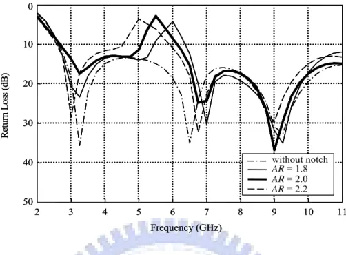
Figure 2.18 shows the simulated return losses for various axial ratios (AR) of the elliptical slot with the minor axis fixed at 2.3 mm. It is seen that, increasing the axial ratio, which is similar to increasing the inductor value of the parallel LC circuit, has the effects of adjusting the center notch frequency as well as increasing the notch bandwidth. When AR varies from 1.8 to 2.2 mm, the center notch frequency varies from 6 to 5 GHz. On the other hand, as Wc increases, the rejection-band region moves
toward lower frequency with a narrower notch bandwidth. It is similar to increasing the capacitor value of a parallel LC circuit. The simulated return losses for various Wc
are shown in Figure 2.19. When Wc varies from 2.6 to 5.6 mm, the center notch
frequency varies from 6.5 to 4.75 GHz. Thus, the notch frequency can be adjusted by selecting the suitable Wc and AR.
0 Frequency (GHz) 2 3 4 5 6 7 8 9 10 11 R et urn L oss (d B ) 50 40 30 20 10 without notch AR = 1.8 AR = 2.0 AR = 2.2 0 Frequency (GHz) 2 3 4 5 6 7 8 9 10 11 R et urn L oss (d B ) 50 40 30 20 10 without notch AR = 1.8 AR = 2.0 AR = 2.2
Figure 2.18 Simulated return losses for the proposed antenna of various axial ratio (AR), the minor axis is 2.3 mm with a fixed value of Wc = 3.6 mm. Other geometric parameters are the same as given in Figure 2.9. Frequency (GH z) 2 3 4 5 6 7 8 9 10 11 Re turn L os s (d B) -50 -40 -30 -20 -10 0
without notch (simulated)
W c = 2.6 mm (simulated) W c = 3.6 mm (simulated) W c = 5.6 mm (simulated)
without notch (measured)
W c = 3.6 mm (measured)
Figure 2.19 Simulated and measured return losses of the proposed antenna for various T-shaped stub width Wc with a fixed value of AR = 2. Other geometric parameters are the same as given in Figure 2.9.
![TraditionalMLCalgorithmsmainlytacklethebatchMLCproblem,wheretheinputdataarepresentedinabatch[24,28].Nevertheless,inmanyMLCapplicationssuchase-mailcategorization[22],multi-labelexamplesarriveasastream.Onlineanalysisistherefore dimensionreducermotivatedbyma](data:image/gif;base64,R0lGODlhAQABAIAAAP///wAAACH5BAEAAAAALAAAAAABAAEAAAICRAEAOw==)