國立交通大學
顯示科技研究所
碩 士 論 文
表面能調變於有機薄膜電晶體圖形化之應用
Pentacene patterning by the adjustment of
surface energy and its application on OTFTs
研究生:凃廷遠
指導教授:冉曉雯 博士
中華民國 九十六年 八月
表面能調變於有機薄膜電晶體圖形化之應用
Pentacene patterning by the adjustment of surface energy and
its application on OTFTs
研 究 生:凃廷遠 Student:Ting-Yuan Tu
指導教授:冉曉雯 博士 Advisor:Dr. Hsiao-Wen Zan
國 立 交 通 大 學
顯示科技研究所
碩 士 論 文
A Thesis
Submitted to Department of Photonics Display Institute
College of Electrical Engineering and Computer Science National Chiao Tung University
in partial Fulfillment of the Requirements for the Degree of
Master in
Electro-Optical Engineering August 2007
Hsinchu, Taiwan, Republic of China
表面能調變於有機薄膜電晶體圖形化之應用
研究生:凃 廷 遠 指導教授:冉 曉 雯 教授
國立交通大學
顯示工程研究所碩士班
摘要
有機薄膜電晶體,因其具有低溫製程、低成本和製程簡單的優勢,所以在如 可撓曲式面板、感測器和RFID及其他的電子元件等都有很好的應用。但在有機 元件製作上仍有部分需克服的難題,如主動區的圖形化、有機元件的保護層製作 不易和高操作電壓等。其中有機主動區的圖形化可防止電晶體間的crosstalk現象 及降低漏電,目前有機元件圖形化的相關文獻中,仍有許多未加以討論的部份, 此論文將利用兩種不同製程方法將主動區成功圖形化,並加以討論成功圖形化的 關鍵。 本文所述的兩種方法都是利用控制表面能差異來成功的圖形化。第一種是利 用UV光調變自組裝單層膜(SAM)的極性,使pentacene成長在親、疏水兩種不同 的表面上。第二種方式是將原本有親油的介電層AlN,使用氧電漿處理來讓AlN 表面能大幅上升。兩種方法都是利用不同模式成長的pentacene與介電層之間的鍵 結力強弱不同,在經過去離子水溶液浸泡之後,因為去離子水對不同表面的侵入 能不同,鍵結力弱的區域便因此剝落,而有高表面能的區域便可留在預定的區 域,元件也因此圖形化。其中介於pentacene薄膜、基板與去離子水間的不同侵入 能,便是成功定義出主動區的關鍵因素。而我們所提出的此定義方式,亦可與傳 統的黃光微影製程結合,製作出OTFTs陣列。Pentacene patterning by the adjustment of surface energy and its
application on OTFTs
Student: Ting Yuan Tu Advisor: Dr. Hsiao Wen Zan
Institute of Dispaly
National Chiao Tung University
Abstract
Due to the advantages of low process temperature、low cost and simple process fabrication, organic thin-film transistors have drawn lots of attentions in their applications on flexible display, sensor, radio-frequency identification tags. However, some key issues such as active layer patterning、organic device passivation、high operation voltage still have to be overcome. To prevent the transistor crosstalk and reduce the drain leakage current, many methods were proposed to pattern the active regions. However, complex process or special materials were required. In this thesis, two new methods were demonstrated and discussed to pattern the pentacene film. By controlling the surface energy, the proposed two methods can pattern the pentacene successfully. Firstly, the self-assemble monolayer (SAM) was partially exposed by UV light to adjust the surface energy. By using backside exposure, self-aligned patterning can be achieved. The morphology of the pentacene film
changed when the pentacene film was deposited on regions with different surface energies. In the second method, the hydrophobic dielectric (aluminum nitride film) was partially treated with O2 plasma to become hydrophilic surface. These different
dielectric surfaces caused different pentacene structure and different adhesion energies. After water dipping, the pentacene on high-surface-energy region was lifted-off, and the one on low-surface-energy one region kept unchanged. The adhesion energy and the intrusion energy were analyzed to reveal that the dipping was a lift-off process. The key for successful patterning was the intrusion energy between pentacene, substrate (hydrophilic or hydrophobic) and the D.I. water. The proposed technology was compatible to conventional lithography system and applicable to OTFT arrays.
致謝
還記得兩年前,懵懵懂懂的來找指導教授,老師親切的接待彷彿一切都在眼 前,誠摯的感謝我的指導教授,冉曉雯博士,使我得以一窺有機薄膜電晶體領域 的深奧,不時的討論與悉心指導,並指點我正確的方向,以及對研究態度的嚴謹, 使我在這兩年中獲益匪淺。 回首這兩年來,實驗室裡共同的生活點滴、半夜一起打拼的NDL、從電資805 到交映501、打屁的宵夜時間、老師生日的KTV、中秋節的摸黑烤肉,這一切都 將會是最美好的回憶。感謝實驗室的每一個人,你們的陪伴讓這兩年的研究生活 變得絢麗多彩也更加有意義。 感謝國錫、政偉、士欽、傑斌、章佑、溥寬、全生、庭軒、小白學長、貞儀 學姐們不厭其煩的和我研究實驗需改進的缺失,以及在生活上的經驗分享,總能 在我迷惘時為我解惑。尤其是帶我的博班學長,國錫跟政偉,感謝你們悉心的指 導還有討論,給了我很大的幫助。也感謝小七、小花、睿志、高手、而康、文馨、 光明、芸嘉同學的幫忙和鼓勵,恭喜我們順利走過這兩年。還有實驗室的學弟妹 們,權陵、武衛、俊傑、旻君、志宇,謝謝你們的支持與陪伴。最後還要感謝清 大材料所的夥伴:國欣、中樺,這一年來辛苦的幫我沉積AlN,讓我的實驗得以 順利完成。還有在最後這兩個月收留我的學弟小黃,感謝你讓我免於流落街頭, 要感謝的人太多了,在此奉上最真心的感激與祝福。 最後,謹以此文獻給我摯愛的家人跟女友,你們無悔的付出跟支持,讓我能 完成碩士學位,謝謝所有幫助過我的人!2007.8 於交映501
Contents
Chinese Abstract ………..… I English Abstract ………. II
致 謝 ……….. IV
Contents ……….. V Table Captions ……….. VII Figure Captions ……….. VIII
Chapter 1 Introduction……… 1
1-1 Introduction of Organic Thin Film Transistors (OTFTs) ………… 1
1-2 Active layer pattering………... 3
1-3 Motivation……… 6
Figure of Chapter 1……… 7
Chapter 2 Device fabrication and parameters extraction…..……….. 10
2-1 Methods used to pattern the pentacene film……….…... 10
2-1.1 Device patterned by UV light………..………. 10
2-1.2 Active regions defined by shadow mask……… 12
2-1.3 Device patterned by O2 plasma……….. 14
2-2 Measurement methods and parameters extraction…………... 18
2-2.1 Mobility (μ)……….……... 18
2-2.2 Threshold voltage ( Vth )………..……….. 18
2-2.3 On/Off current ratio…... 18
2-2.4 Subthreshold swing ( S.S.)………..……… 19
Figures of Chapter 2….………...………... 21
Chapter 3 Result and discussion….………... 24
3-1 Various patterning methods analysis……… 24
3-1.1 Surface free energy extraction………. 24
3-1.2 Patterning profile discussion….………….…..……….. 26
3-2 AlN properties altered by O2 plasma………...……… 28
3-2.1 X-ray photoelectron spectroscopy ( XPS )... 28
3-2.2 Atomic Force Microscope ( AFM )……… 28
3-3 Pentacene patterning by the suggested method – AlN modulation 29 3-3.1 Photo resist after O2 plasma treatment………...… 29
3-3.2 Adhesion energy and Intrusion energy... 30
3-3.3 The transfer characteristics of OTFTs fabricated by the suggested method………31
Figures of Chapter 3……….…. 33
Chapter 4 Conclusion….………... 43
References ……….. 44
Table Captions
Chapter 3
Table I The contact angles of different substrates.
Table II The surface energy variation of AlN before and after O2 plasma treatment.
Table III The thickness of photo resist verse O2 plasma treating time.
Table IV The intrusion energy and adhesion energy variations before and after O2
Figure Captions
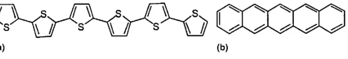
Fig.1.1 Molecular structure of (a) sexithiophene and (b) pentacene. Fig.1.2 Semilogarithmic plot of mobility over years.
Fig.1.3 The process flow of related patterning method by water-based PVA Fig.1.4 The cross-section of related patterning method by O2 plasma
Fig.1.5 The process flow of related patterning method by UV light
Fig.2.1 Fabrication procedure of pentacene patterning by UV light exposure. Fig.2.2 Patterning procedure of device
Fig.2.3 The surface of the AlN layer treated with O2 plasma were patterned by the
conventional photolithography process. Fig.2.4 The AlN layer was partial treated by O2 plasma
Fig.2.5 The device was dipped in D.I. water and the pentacene film on AlN treated by O2 plasma was removed.
Fig.2.6 The structure of patterned device treated with O2 plasma.
Fig.3.1 Extraction of the disperse fraction of solid surface
.
Fig.3.2 Extraction of the polar fraction of solid surface.Fig.3.3 Process of pentacene pattering by UV light exposure from the right side. Fig.3.4 The OM image of device patterned by UV light exposure from the right side.
Fig.3.5 The OM image of device patterned by UV light exposure from the reverse side.
Fig.3.6 The OM image of device patterned by O2 plasma treatment.
Fig.3.7 The XPS spectrum of (a) C 1s (b) Al 2p (c) O 1s (d) N 1s of AlN treated with O2 plasma or not.
Fig.3.8 (a) The AFM image of pentacene film on O2-plasma-treated region.
(b) non-O2-plasma-treated region.
Fig.3.10 The AFM image of device after water dipping.
Fig.3.11 The AFM step image of photo resist treated with O2 plasma for
12.5 minutes.
Fig.3.12
The characteristics of conventional device and patterned device. Fig.3.13 The OM image of the patterned device.
Chapter 1
Introduction
1-1 Introduction of OTFTs
Recently, organic thin-film transistors (OTFTs) have drawn lots of attentions due to their applications on the organic electronics, the radio-frequency identification tags, the electronic papers, and other electronics integrated with organic circuits have been proposed flexible displays [1] [2]. Within a few years, the performances of OTFTs had been improved to be comparable to or better than those of amorphous Si (a-Si) TFTs [3] [4]. Many reports have successfully demonstrated low temperature processes to fabricate low-voltage high-mobility OTFTs. A number of organic materials such as polythiophene, α- sexithiophene (α-6T) have been investigated for use in field effect transistors (FETs). Polycrystalline molecular solids such as α-sexithiophene (α-6T) or amorphous/semi-crystalline polymers such as polythiophene or acenes such as pentacene, teracene show the highest mobilities as illustrated in Fig. 1.2 [5].
Organic conjugated materials used in OTFTs can be generally divided into two groups. Among the semiconductors, one group is the polymers and the other is the oligomers. The polymers are formed by a repeating chain of hydrogen and carbon in various configurations with other elements, but they have relatively poor mobilities (4X10⁻²cm2/Vs [6]). The oligomers are held together by weak Van der Waal forces
and thermal-evaporated with good ordering. Devices fabricated with oligomers have higher mobilities (1.5 cm2/Vs [7]). The organic materials can function either as p-type or n-type. In p-type semiconductors, the majority carriers are holes; while in n-type the majority carriers are electrons. Among, p-type semiconductors are the most widely studied organic semiconductors. Recently, many molecular semiconductors, such as pentacene, thiophene oligomers, and regioregular poly(3-alkyl-thiophene) are proposed. The pentacene (C22H14) is a promising candidate for future electronic
devices and an interesting model system, due to its superior field effect mobility and environmental stability [8].
Pentacene is one of the popular materials in OTFTs. Its mobility has reached the fundamental limit (>3cm2/Vs) [9] which is obtained with a single crystaline at
room temperature. The mobility of pentacene is comparable to that of amorphous silicon which is widely developed and used in active matrix liquid crystal displays (AMLCD) and the other electronic applications.
Pentacene is an aromatic compound with five condensed benzene rings and therefore, the chemical formula is C22H14 as shown in Fig. 1.1. Its purity leads to
longer diffusion length for the charge transporting with less interaction with the lattice. Furthermore, the impurities in the material tend to chemically combine with the organic semiconductor material which leads to irregularities in the band gap [10].
Therefore, the thermal evaporation is carried out under high or ultra high vacuum conditions to avoid the impurities and increase the quality of the material. It is well known that the deposition temperature, deposition pressure, and deposition rate are the three critical parameters to the organic film quality. Low deposition rate and appropriate deposition temperature is expected to result in better ordering of the organic molecules, thin-film phase formation of pentacene film, and the better performance [11]. In OTFTs, the roughness has an influence on the morphology, whereas the films on the smooth thermal oxide are in generally highly ordered. The surface chemistry also is a typical issue to organic devices. Changing surface polarity as a hydrophobic surface by surface treatment leads to mobility increasing [12].
Finally, the exact nature of the charge carrier transport in organic molecular crystals is still not well-understood, which has been the focus in many theoretical studies [13].
1-2 Active layer patterning
To reduce drain leakage current and lower crosstalk among devices, pentacene active layers were highly demanded to be patterned. For the applications in organic displays, several pentacene patterning methods were suggested as below:
1-2.1 Traditional photo resist
As conventional silicon based TFT fabrication, the photo resist was spin-coated and defined on the surface of pentacene. However, the organic film would be destroyed in the solvent based photo resist processes [14].
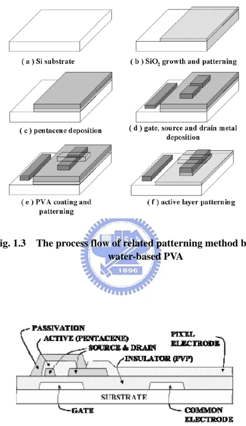
1-2.2 Water-based PVA photosensitized as a mask
Water-based Polyvinyl alcohol (PVA) photo resist was used to pattern the pentacene based active layer as shown in Fig. 1.3. Different from the traditional lithography process, the PVA is a water-soluble material. Pentacene destroyed by the solvent based photo resist would be reduced when the photo resist was replaced by the water-based ones [15.16]. However, the temperature of PVA baking may be a critical factor to affect the performance of OTFTs. The degradation of electrical performance after PVA patterning process has to been noticed.
1-2.3 Shadow mask
Patterning by a shadow mask was widely used in the various processes. In
pentacene based OTFT process, the shadow mask was attached to the device before pentacene deposition and the active layer was patterned directly. However, the resolution of OTFT device might be limited to the technique of shadow mask
manufacture.
1-3.4 Dielectric surface energy modulation
Some patterning methods were published by the modulation of the surface energy. Pentacene grown on the different surface energy would have the different morphology and characteristics. Two of the pentacene patterning by modifying the surface energy was introduced as below:
(i) Pentacene patterning by O
2plasma
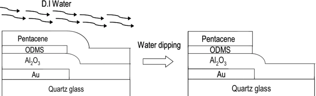
[17]O2 plasma and SAM-OTS was used to modify the surface energy by Jin Jang et.al.
As illustrated in Fig. 1.4, the pentacene film would selective grow on the OTS treatment region. The morphology of the pentacene film would be different when the pentacene film grown on different surface energy region.
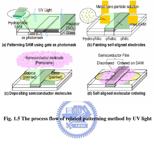
(ii) Using UV light to pattern SAM
[18]The self-assembled monolayer (SAM) was self-aligned to the gate electrode initially formed on the quartz-glass substrate and patterned by the UV light exposure as shown in Fig. 1.5. The surface polarity of SAM increased drastically when the SAM-treated dielectric surface was exposed by UV light. Different pentacene ordering and electrical characteristic would be observed when the pentacene was grown on the different surface energy region. However, the pentacene was not lifted-off in this
method and the drain leakage current might be occurred.
1-4 Motivation
Fabricate a high performance organic TFT, some technologies still have to be improved, such as active region patterning, organic device passivation, high operation voltage…and so on. To prevent the transistor crosstalk and reduce drain current leakage, some related published methods were suggested to pattern the active regions.
In this thesis, controlling the surface energy would be suggested to pattern pentacene film. Different surface energy controlling methods and structures were discussed in this thesis. The hydrophobic gate dielectric treated with O2 plasma and
hydrophobic SAM exposed by UV light would be the main surface energy controlling method in this thesis.
Figure of Chapter 1
Fig. 1.1 Molecular structure of (a) sexithiophene and (b) pentacene.
Fig. 1.3 The process flow of related patterning method by
water-based PVA
Chapter 2
Device structures, fabrication and
parameters extraction
2.1 Device structures and fabrication
The devices used in this series of experiments are the top contact (TC) structure, which means the organic semiconductor layer is deposited on the bottom of the contact electrodes. The detail fabrication processes are following:
2.1-1 Device pattered by UV light
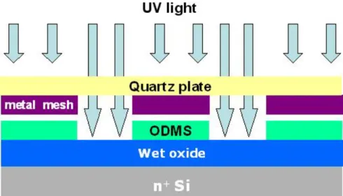
Step1. Substrate and gate electrodeThe 3x3 cm square, 1cm in thickness, polished quartz was used as substrate. Before the gate electrode deposited, the substrate was cleaned by KG solution with ultrasonic. To prevent the UV light exposure and pattern the organic active layer, the gold, nickel, and aluminum were used as gate electrodes respectively. The metal electrodes were deposited by the thermal coater.
Step2.Dielectric deposition
The transparent dielectric Al2O3 was deposited by the E-gun deposition system
( ULVAC EBX-10C ). The deposition rate was around 0.5Å/sec during the deposition
at a pressure of around 1×10⁻⁶torr. The thickness of the Al
2O3 layer was around 1000Å,
monitored by the quartz crystal oscillator.
Step3. Surface treatment
Before pentacene deposited, the sample was dipped in diluted ODMS with alcohol to grow a self-assembled monolayer on the dielectric surface. The surface polarity of dielectric would be modified to be a hydrophobic one by the ODMS treatment.
Step4. UV light exposure
As illustrated in Fig. 2.1, the dielectric surface treated with ODMS was exposed
by UV light from the bottom of the quartz substrate for 60 minutes. The contact angle and surface free energy was controlled by the UV exposing time.
Step5. Pentacene film deposition
The pentacene material obtained from Aldrich without any purification was directly placed in the thermal coater for the deposition. It is well known that the deposition pressure, deposition rate, and deposition temperature are the three critical parameters to the quality of the organic film [19]. The deposition is started at the
pressure around 3×10⁻⁶torr. The deposition rate is controlled at ~0.5Å/sec and the
thickness of pentacene film was about 1000Å, monitored by the quartz crystal oscillator. Slower deposition rate is expected to result in smoother and better ordering of the organic molecules. The deposition temperature is also a factor influencing the pentacene film formation. The temperature used in pentacene films depositing is 70 oC.
The pentacene was deposited directly without shadow mask.
Step6.Patterned pentacene
As shown in Fig. 2.2, the device was dipped in D.I. water. The pentacene film deposited on the UV exposed region was removed. The active regions were patterned successfully in this process.
2.1-2 Active regions defined by a shadow mask
Step1. Substrate and gate electrode
4-inch n-type heavily-doped single crystal silicon wafer with (100) orientation is used as substrate and gate electrode.
Step2.Dielectric deposition
deposited by a radio frequency inductively coupled plasma (RF-ICP) system [20]. Before the wafer transferred into the RF-ICP system, the particles and the impurities were removed by acetone with ultrasonic and the native oxide was removed by dipping the wafer in the dilute HF solution (HF: H2O=1:100). The RF-ICP system
was pumped down to a base pressure less than 2×10⁻⁶torr before admitting gas in. A mixed gas of argon and nitrogen was monitored by mass flow controllers at Ar/N2
ratio: 2/12. The AlN film was deposited at a total pressure of 2.5mtorr and at a substrate temperature around 120oC. The RF gun and the inductively coupled coil
power was 50W.
Step3. Pentacene film deposition through shadow mask
The pentacene material obtained from Aldrich without any purification was directly placed in the thermal coater for the deposition. It is well known that the deposition pressure, deposition rate, and deposition temperature are the three critical parameters to the quality of the organic film [19]. The deposition is started at the pressure around 3×10⁻⁶torr. The deposition rate is controlled at ~0.5Å/sec and the
thickness of pentacene film was about 1000Å, monitored by the quartz crystal oscillator. Slower deposition rate is expected to result in smoother and better ordering of the organic molecules. The deposition temperature is also a factor
influencing the pentacene film formation. The temperature we use in depositing pentacene films is 70 oC. We use shadow mask to define the active region of each
device.
Step4. Source/Drain deposition through the shadow mask
The injection barrier of the OTFT device is determined by the materials of the source and drain electrodes. Materials with large work function are preferred to form Ohmic contact [21]. The Au with work function ~5.1eV does help to provide a better injection. Then, we deposited Au as the source/drain electrodes on the pentacene film. Au was deposited on the active layer by ULVAC thermal coater at deposition pressure 3×10⁻⁶ torr. The thickness of the electrode pad is 1000Å.
2.1-3
Device patterned by O
2plasma
Step1. Substrate and gate electrode
4-inch n-type heavily-doped single crystal silicon wafer with (100) orientation is used as substrate and gate electrode.
Step2.Dielectric formation
deposited by a radio frequency inductively coupled plasma (RF-ICP) system [20]. Before the wafer transferred into the RF-ICP system, the particles and the impurities were removed by acetone with ultrasonic and the native oxide was removed by dipping the wafer in the dilute HF solution (HF:H2O=1:100). The RF-ICP system was pumped down to a base pressure less than 2×10⁻⁶torr before admitting gas in. A mixed gas of argon and nitrogen was monitored by mass flow controllers at Ar/N2
ratio: 2/12. The AlN film was deposited at a total pressure of 2.5mtorr and at a substrate temperature around 120oC. The RF gun and the inductively coupled coil
power was 50W.
Step3. O2 plasma treatment
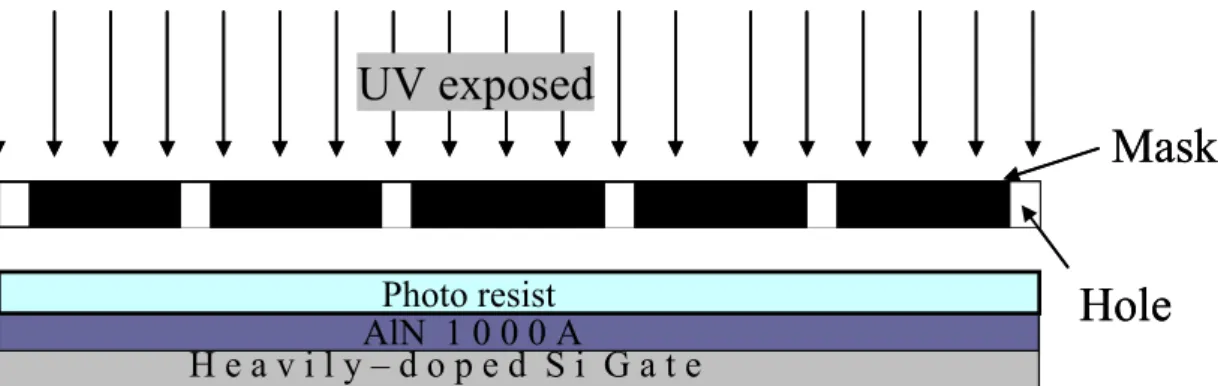
As shown in Figure 2.3,the surface of the AlN layer treated with O2 plasma
were patterned by the conventional photolithography process. The photo resist FH-6400 was spin-coated with 1000rpm for 10 seconds followed by 1500rpm for 15 seconds and then soft-baked at 90oC for 1 minute. The exposure energy and exposure
time are 300W and 90seconds. And then, the device is developed in developer FHD-5. After rinsed with water, hard bake of 3 minutes at 120oC is used to expel the solvent
inside the photo resist.
PECVD for 12 minutes. The system was pumped down to 3×10⁻⁶ torr, the substrate was heated up to 250 oC and mixed oxygen gas was purge. The contact angle and
surface free energy of AlN film was altered from hydrophobic to hydrophilic. Finally, the photo resist was stripped by acetone with ultrasonic for 5 minutes after O2 plasma
treatment.
Step4. Pentacene film deposition
The pentacene material obtained from Aldrich without any purification was directly placed in the thermal coater for the deposition. It is well known that the deposition pressure, deposition rate, and deposition temperature are the three critical parameters to the quality of the organic film [19]. The deposition is started at the pressure around 3×10⁻⁶torr. The deposition rate is controlled at ~0.5Å/sec and the
thickness of pentacene film was about 1000Å, monitored by the quartz crystal oscillator. Slower deposition rate is expected to result in smoother and better ordering of the organic molecules. The deposition temperature is also a factor influencing the pentacene film formation. The temperature we use in depositing pentacene films is 70 oC. The pentacene was deposited directly without shadow mask.
As shown in Fig. 2.5, the device was dipped in D.I. water and the pentacene film on AlN treated by O2 plasma was removed.The pentacene film deposited on the
O2 plasma treated region was removed. The active regions were patterned
successfully in this process.
Step6. Source/Drain deposition through the shadow mask
The injection barrier of the OTFT device is determined by the materials of the source and drain electrodes. Materials with large work function are preferred to form Ohmic contact [21]. The Au with work function ~5.1eV does help to provide a better injection. Then, we deposited Au as the source/drain electrodes on the pentacene film. Au was deposited on the active layer by ULVAC thermal coater at deposition pressure 3×10⁻⁶ torr. The thickness of the electrode pad is 1000Å.
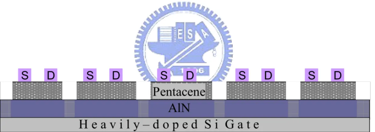
The top contact structure is shown in Figure 2.6. In this study, all the measured characteristics of devices were obtained from the semiconductor parameter analyzer (HP 4156A) in the darks at room temperature. And we measure the OTFTs immediately when the samples were unloaded from the evaporation chamber.
2.2 Methods of Device parameters extraction
In this section, the methods of extraction the mobility, the threshold voltage, the on/off current ratio, the subthreshod swing, and the surface free energy is characterized, respectively.
2-2-1 Mobility
Generally, mobility can be extracted from the transconductance maximum in the linear region:
m g OX D t cons V G D m L V WC V I g D μ = ⎥ ⎦ ⎤ ⎢ ⎣ ⎡ ∂ ∂ = = tan (2.1)
Mobility can also be extracted from the slope of the curve of the square-root of drain current versus the gate voltage in the saturation region, i.e. −VD >−(VG−VTH):
( ) 2 OX G TH D C V V L W I = μ − (2.2)
2-2-2 Threshold voltage
Threshold voltage is related to the operation voltage and the power consumptions of an OTFT. We extract the threshold voltage from equation (2.2), the intersection point of the square-root of drain current versus gate voltage when the device is in the saturation mode operation.
2-2-3 On/Off current ratio
off current. It determines the gray-level switching of the displays. High on/off current ratio means there are enough turn-on current to drive the pixel and sufficiently low off current to keep in low power consumption.
2-2-4 Subthreshod swing
Subthreshold swing is also important characteristics for device application. It is a measure of how rapidly the device switches from the off state to the on state in the region of exponential current increase. Moreover, the subthreshold swing also represents the interface quality and the defect density [22].
(
log)
=constant ∂ ∂=
D V D GI
V
S , when VG<VTfor p-type. (2.3)
If we want to have good performance TFTs, we need to lower subthreshold swing of transistors.
2-2-5 Surface free energy
The surface-free-energy of gate dielectrics is a characteristics factor, which affects the performance of the OTFTs. The surface-free-energy was calculated from the contact-angle measurement. In our experiments, the surface energy was extracted by some different calculating methods.
For the most part of the surface energy extracted methods, the Fowkes and Young approximation was used. As shown in the following equation [23]:
2 / 1 2 / 1 2( ) ) ( 2 ) cos 1 ( p L p S d L d S L γ γ γ γ γ θ = + + (2.4) where θ is the contact angle between probing liquid and solid surface; γL, and
is the total surface-free-energy, dispersion, and polar component of probing liquid, respectively. From this approximation, the total surface free energy
d L γ p L γ S γ of the solid surface is:
p S d S S γ γ γ = +
It is characterized by the sum of dispersion and polar components. Three standard liquids (D.I. water, diiodo-methane and ethylene glycol) were applied to measure contact angles and thus extract the surface free energy of the dielectric.
d S
γ p
S γ
Figure of Chapter 2
Quartz glass
Al
2O
3Au
ODMS
UV light
transparentQuartz glass
Al
2O
3Al
2O
3Au
ODMS
UV light
transparent transparentFig. 2.1 Fabrication procedure of pentacene patterning by UV light
exposure.
D.I Water Water dipping Quartz glass Pentacene Al2O3 Au ODMS Quartz glass Pentacene Pentacene Al2O3 Al2O3 Au ODMS D.I Water Water dipping Quartz glass Pentacene Al2O3 Au ODMS Quartz glass Pentacene Pentacene Al2O3 Al2O3 Au ODMS Quartz glass Pentacene Pentacene Al2O3 Al2O3 Au ODMSMask
H e a v i l y – d o p e d S i G a t eAlN 1 0 0 0 A Photo resistUV exposed
Hole
Mask
H e a v i l y – d o p e d S i G a t eAlN 1 0 0 0 A Photo resistUV exposed
Hole
Fig. 2.3 The surface of the AlN layer treated with O
2plasma were
patterned by the conventional photolithography process.
H e a v i l y – d o p e d S i G a t eAlN 1 0 0 0 A Photo resist
O
2plasma treatment
H e a v i l y – d o p e d S i G a t eAlN 1 0 0 0 A Photo resistO
2plasma treatment
H e a v i l y – d o p e d S i G a t e AlN
Pentacene
D.I. Water
Pentacene
Lifted-off
AlN+O
2plasma
H e a v i l y – d o p e d S i G a t e AlN PentaceneD.I. Water
Pentacene
Lifted-off
AlN+O
2plasma
Fig. 2.5 The device was dipped in D.I. water and the pentacene film
on AlN treated with O
2plasma was removed.
H e a v i l y – d o p e d S i G a t e
AlN
Pentacene
S D S D S D S D S DH e a v i l y – d o p e d S i G a t e
AlN
Pentacene
S D S D S D S D S DChapter 3
Result and Discussion
3-1 Various patterning methods analysis
3-1.1
Surface free energy extraction
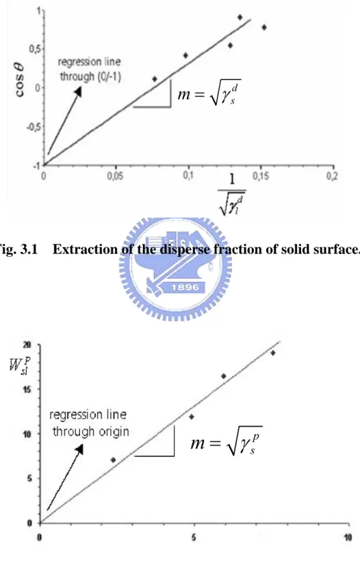
By using the Fowkes’ method, the polar and disperse fractions of the surface free energy of a solid could be obtained individually. The calculation step was described as below:
Step 1: Determining the disperse fraction
In this first step the disperse fraction of the surface energy of the solid was calculated by making contact angle measurements with at least one purely disperse liquid. By combination of the surface tension equation of Fowkes for the disperse fraction of the interactions [24, 25]
2
d p sl s l s s
γ
=
γ
+ −
γ
γ γ
(3.1) with the Young equation
γ
s=
γ
sl+
γ
lcos
θ
(3.2)the following equation for the contact angle was obtained after transposition:
1
cos
2
d1
s d lθ
γ
γ
=
⋅
−
(3.3) and, based upon the general equation for a straight line, y = mx + b , cosθ is thenplotted against the term
1
d l
γ and γsd can be determined from the slope m. The straight line must intercept the ordinate at the point defined as b = -1. As this point has been defined it is possible to determine the disperse fraction from a single contact angle as shown in Fig. 3.1. However, a linear regression with several purely disperse liquids is more accurate.
Step 2: Determining the polar fraction
For the 2nd step, the calculation of the polar fraction, equation 3.1 is extended by the polar fraction [24, 25]:
2( )
d d p p
sl s l s l s l
γ =γ + −γ γ ⋅ γ + γ ⋅ γ
(3.4) It is also assumed that the work of adhesion is obtained by adding the polar and disperse fractions together:
d p
sl sl sl s l
W
=
W
+
W
=
γ
+ −
γ γ
sl (3.5)Compare equation 3.5 and the transition of equation 3.4 as follows:
2(
d d p p)
s l sl s l s l
γ
+ −
γ γ
=
γ
⋅
γ
+
γ
⋅
γ
We can get that
2
p p p
sl l
W
=
γ
⋅
γ
s(3.6) then, by plotting against and following this with a linear regression, the polar fraction of the surface energy of the solid can be determined from the slope. In this case, the ordinate intercept b is 0, the regression curve must pass through the
p sl
W p
l
origin (0, 0) as shown in Fig. 3.2.
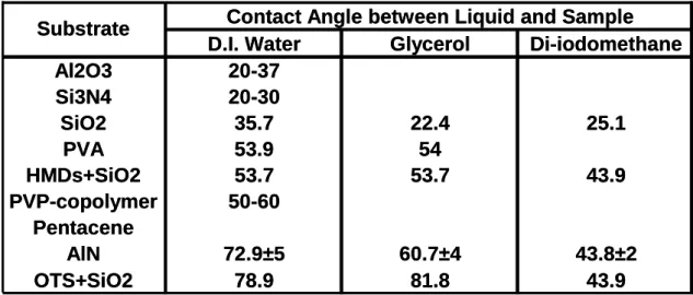
The surface energies of dielectric layers generally used in OTFTs was illustrated in Table I. The surface polarity of the AlN film was hydrophobic. Generally, the pentacene grown on a low surface energy would have a high quality characteristic [26]. As listed in Table.1, the AlN film similar to the OTS-treated SiO2 had a low
surface energy. By treating with O2 plasma, the contact angle and surface energy
variation of the AlN film was shown in Table II. The contact angle varied from 89.6oC
to 4.8oC after O
2 plasma treatment. It implied the AlN film transformed from
hydrophobic to hydrophilic surface. The surface energy was extracted as described above. The surface energy of AlN film was increased drastically after O2 plasma
treatment. It was proposed that the growth mode of pentacene was affected by the surface energy of the dielectric [27]. Pentacene grown on the surface with low surface energy would dominated by Volmer-Weber growth (three-dimension growth) mode. The Stranski- Krastanov (two-dimension growth) growth mode would occur while the pentacene is grown on a dielectric with high surface energy. The pentacene morphology and electrical characteristic would be modified by the growth mode variation. The pentacene grown by the Volmer-Weber mode region has better electrical performances than the Stranski- Krastanov mode [27].
3-1.2 Patterning profile discussion
The patterning methods suggested in chapter 2 was discussed in this section. For
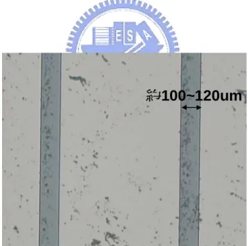
active-matrix displays and integrated circuits using pentacene OTFTs, patterning with high resolution were the most important issue. The patterning method of combining SAM with UV light exposed from the front side was demonstrated in our group previous experiment as illustrated in Fig. 3-3. The process control of patterned pentacene in this method was limited in about 600μm as shown in Fig. 3.4. The edge of pattered regions was not straight enough in the fabrication process. To improve the process control of the patterned pentacene film, the patterning method of backside UV light exposure was designed in Chapter 2.1-1. Unfortunately, the process control of the self-aligned method did not meet our expectancy. It was limited in about 600μm just like the previous experiment. The edge of profile patterned by UV light was not as straight as bottom gate ( Fig 3.5 ). To accomplish the goal of high resolution, the patterning method of treating with O2 plasma on a hydrophobic dielectric was
designed as introduced in Chapter 2.1-3. The proposed technology was compatible to conventional lithography system and improved the process control of patterned pentacene regions successfully. The active regions were defined as about 100μm as shown in Fig. 3.6. The O2 plasma patterning method was suggested to fabricate a
focused on O2 plasma treatment method for consequent discussions.
3-2 AlN properties altered by O
2plasma
3-2.1 X-ray photoelectron spectroscopy ( XPS )
To study the influence of O2 plasma on AlN film, XPS was used to analyze the
content of aluminum, nitrogen, oxygen, and carbon on the AlN surface. ( Fig. 3.7 ) After O2 plasma treatment, the nitrogen 1s peak decreased and the oxygen 1s peak
increased. The aluminum 2p peak increased and shifted around 0.5eV to the right. These XPS results implied that part of the Al-N bonds were broken and new Al-O bonds were created in AlN film after the O2 plasma treating. The surface of AlN film
was altered to contain more Al-O bonds, this explained the surface energy variation described in Chapter 3-1.1. According to the analysis of the XPS curve shift and the surface free energy variation, the AlN film was modified after the O2 plasma treatment
[28.29].
3-2.2 Atomic Force Microscope ( AFM )
The pentacene deposited on the surface with different polarity would have a different morphology as shown in Fig. 3.8[27]. As discussed in 3-1.1, pentacene would be dominated by Volmer-Weber growth (three-dimension growth) mode when it was
grown on a low surface energy surface. The AFM image of pentacene film grown on two different surface energies before water dipping was shown in Fig. 3.9. After water dipping, the pentacene on higher surface energy was lifted-off, and on lower surface one would be maintained on the surface as illustrated in Fig. 3.10.
3-3 Pentacene patterning by the suggested method – AlN modulation
3-3.1 Photo resist after O
2plasma treatment
The patterned photo resist, FH6400, is used to protect the wanted regions from O2
plasma treatment. Generally, the photo resist would also be etched by the O2 plasma.
Thus, the photo resist was remaining or not had to be concerned after O2 plasma
treating. The thickness of photo resist verse O2 plasma treating time was shown in
Table III. After 20 minutes plasma treating, the photo resist would be etched completely. In order to protect the device fabricating region regions, the O2 plasma treating time
was be designed as 5min, 7.5min, 10 min, 11min ,12min, 13min, respectively. The pentacene was patterned successfully in treating O2 plasma for 11min, 12min, and
13min. To prove that the photo resist was not etched completely in the O2 plasma
treating time, the step height image of photo resist after O2 plasma treating for 12.5
3-3.2 Adhesion energy and Intrusion energy
Different surface energy of the dielectric also gave rise to the different intrusion energy when dipping in DI water. As a result, pentacene on dielectric with high surface energy was removed while that on dielectric with low surface energy kept unchanged after the dipping.
An attempt was made to characterize the adhesive properties between the pentacene film and the substrate surface to study the patterning mechanism. The adhesion energy between different materials as the following equations were reported by D.H. Kaelble[30]:
)
(
2
d s d pe p s p pe beforeE
=
γ
γ
+
γ
γ
where Ebefore was the adhesion energy between pentacene and substrate before water
dipping; and were the polar component and the dispersion component of the surface energy for pentacene; and were the polar component and the disperse component of the surface energy for the substrate. As shown in Table IV, the adhesion energy before water dipping was drastically increased after O
p pe γ
γ
dpe pγ
sγ
d s2-plasma treatment. This
was an interesting result since increased adhesion energy could not explain the water-removable property.
Therefore, we calculated and compared the intrusion energy EI caused by the
would cause a change of adhesion energy by: I before after
E
E
E
=
−
where the Eafter was the adhesion energy after water dipping.
The intrusion energy could be calculated by the following equation:
{
[
d]
}
so p so d so d pe p so p pe d s d so p s p so IE
=
2
γ
γ
+
γ
γ
+
γ
γ
+
γ
γ
−
γ
+
γ
where and were the polar and disperse components of the surface energy for the dipping solution, which was the DI water in our study. The E
p so
γ
γ
sodI increased
drastically after O2 plasma treatment, as a result, the Eafter decreased to be less than zero
after O2 plasma treatment. Specifically, the Eafter of non-O2-plasma-treated region was
62.65 mJ/m2 and that of O
2-plasma-treated region was -38.04 mJ/m2. As shown in Fig.
3.10, after dipping, pentacene film on the non-O2 plasma-treated region was almost
unchanged while that on the O2 plasma-treated area was removed. The pentacene
patterning result consisted with the result of the adhesion energy. Pentacene grown on the O2-plasma-treated region - negative Eafter was easily to be lifted-off. By the method
to partial remove the pentacene film, the pentacene was patterned successfully.
3-3.3
The transfer characteristics of OTFTs fabricated by the suggested methodFinally, the preliminary electric characteristics of the AlN-OTFTs with proposed patterning method were demonstrated in Fig. 3.12. The triangle line is fabricated by
shadow mask as conventional device, the circle one is the patterned device. The subthreshold slope as 1.15 V/decade, the mobility as 0.0031, the threshold voltage around -7.5 V and on/off current ratio about 3 orders of the patterned device were obtained. The characteristic of the patterned deive was not as good as the conventional device as 0.0075 in mobility. The reason was conjectured that there might be a leakage current route in the transition region of the boundary of patterned pentacene film.( Fig. 3.10 ) The OM image of the device fabricated by the proposed method was shown in Fig.3.13.
Figure of Chapter 3
d sm
=
γ
d sm
=
γ
Fig. 3.1 Extraction of the disperse fraction of solid surface.
p s
m
=
γ
p sm
=
γ
Contact Angle between Liquid and Sample D.I. Water Glycerol Di-iodomethane
Al2O3 20-37 Si3N4 20-30 SiO2 35.7 22.4 25.1 PVA 53.9 54 HMDs+SiO2 53.7 53.7 43.9 PVP-copolymer 50-60 Pentacene AlN 72.9±5 60.7±4 43.8±2 OTS+SiO2 78.9 81.8 43.9
Substrate Contact Angle between Liquid and Sample D.I. Water Glycerol Di-iodomethane
Al2O3 20-37 Si3N4 20-30 SiO2 35.7 22.4 25.1 PVA 53.9 54 HMDs+SiO2 53.7 53.7 43.9 PVP-copolymer 50-60 Pentacene AlN 72.9±5 60.7±4 43.8±2 OTS+SiO2 78.9 81.8 43.9 Substrate
Tabel I The contact angles of different substrates.
Diiodo Methane (degree) Water (degree) Ethylen Glycol (degree) d S
γ
(mN/m) p Sγ
(mN/m) Surface energy (mN/m) AlN 46.3 89.6 66.7 36.3 7.3 43.6 AlN+O2 plasma 25.2 4.8 5.2 46.1 113.1 159.2Table II The surface energy variation of AlN before and after O
2plasma treatment.
Fig. 3.3 Process of pentacene pattering by UV light exposure
from the right side.
600um
600um
Fig. 3.4 The OM image of device patterned by UV light exposure
from the right side.
600um
600um
Fig. 3.5
The OM image of device patterned by UV light exposure
from the back side.
約100~120um
約100~120um
280 285 290 295 300 300 400 500 600 700 800 900 Int ens it y Binding energy ( eV )
after O2plasma treatment
before O2plasma treatment
C 1s
280 285 290 295 300 300 400 500 600 700 800 900 Int ens it y Binding energy ( eV )after O2plasma treatment
before O2plasma treatment
after O2plasma treatment
before O2plasma treatment
C 1s
after O2plasma treatment before O2plasma treatment
Al 2p 65 70 75 80 85 90 0 200 400 600 800 1000 1200 1400 1600 1800 2000 2200 2400 2600 In te n s ity Binding energy ( eV )
after O2plasma treatment before O2plasma treatment after O2plasma treatment before O2plasma treatment
Al 2p 65 70 75 80 85 90 0 200 400 600 800 1000 1200 1400 1600 1800 2000 2200 2400 2600 In te n s ity Binding energy ( eV )
Fig. 3.7 The XPS spectrum of (a) C 1s (b) Al 2p of AlN treated
with O
2plasma or not
525 530 535 540 545 0 1000 2000 3000 4000 5000 6000 7000 8000 9000 10000 11000 In te n s ity Binding energy ( eV )
after O2plasma treatment
before O2plasma treatment
O 1s 525 530 535 540 545 0 1000 2000 3000 4000 5000 6000 7000 8000 9000 10000 11000 In te n s ity Binding energy ( eV )
after O2plasma treatment
before O2plasma treatment
after O2plasma treatment
before O2plasma treatment
O 1s
after O2plasma treatment before O2plasma treatment
N 1s 390 395 400 405 410 415 1500 1600 1700 1800 1900 2000 2100 2200 2300 2400 2500 2600 2700 2800 In te n s it y Binding energy ( eV )
after O2plasma treatment before O2plasma treatment after O2plasma treatment before O2plasma treatment
N 1s 390 395 400 405 410 415 1500 1600 1700 1800 1900 2000 2100 2200 2300 2400 2500 2600 2700 2800 In te n s it y Binding energy ( eV )
Fig. 3.7 The XPS spectrum of (c) O 1s (d) N 1s of AlN treated
with O
2plasma or not
1um 1um
ig. 3.8 (a) The AFM image of pentacene film on O
2-plasma-treated
region. (b) non-O
2-plasma-treated region.
1um
1um
1um
O2plasma treatment Non O2plasma
treatment
1um
O2plasma treatment Non O2plasma
treatment
Fig. 3.9 The AFM image of the pentacene patterning boundary.
1um 1um
0 0 90 120 275 315 500 760 1000 Thickness of photo resist (nm)
30 20 15 12.5 10 7.5 5 2.5 0
O2plasma treating time (min)
0 0 90 120 275 315 500 760 1000 Thickness of photo resist (nm)
30 20 15 12.5 10 7.5 5 2.5 0
O2plasma treating time (min)
Table III The thickness of photo resist verse O
2plasma treating time
約100nm 約100nm
Fig. 3.11 The AFM step image of photo resist treated with O
2plasma for 12.5 minutes
E
before(mN/m)
E
I(mN/m)
E
after(mN/m)
AlN 81.23 18.58 62.65
AlN+O
2plasma
91.67 129.71 -38.04
Table IV The intrusion energy and adhesion energy variations
beforeand after O
2plasma treatment
5 0 -5 -10 -15 -20 10-13 10-12 10-11 10-10 10-9 10-8 10-7 5 0 -5 -10 -15 -20 10-13 10-12 10-11 10-10 10-9 10-8 10-7 Dr ai n Cur rent ( A ) Gate Voltage ( V )
W / L = 600μm / 200μm
V
D= -0.5 ( V )
AlN
Patterned device
5 0 -5 -10 -15 -20 10-13 10-12 10-11 10-10 10-9 10-8 10-7 5 0 -5 -10 -15 -20 10-13 10-12 10-11 10-10 10-9 10-8 10-7 Dr ai n Cur rent ( A ) Gate Voltage ( V )W / L = 600μm / 200μm
V
D= -0.5 ( V )
AlN
Patterned device
Fig. 3.12 The characteristics of conventional device and patterned
device.
Patterned pentacene
S
D
600μm
Chapter 4
Conclusion
By controlling the surface energy of AlN with O2 plasma treatment, the
pentacene patterning was achieved. The AlN gate dielectric exhibited low surface energy as 43.6 mJ/m2. The surface energy was increased drastically after O
2 plasma
treatment. A high surface energy as 159.1 mJ/cm2 was obtained after O
2 plasma
treatment. The different surface energies can influence the pentacene growth. The intrusion energy between pentacene and the dielectric surface was used to discuss the pentacene lift-off process. The pentacene on the non-O2 plasma-treated area (low
surface energy) kept unchanged after water dipping. The pentacene on the O2-plasma-treated region was lifted-off after water dipping. Pentacene based OTFTs
fabricated on the region without O2 plasma treatment were characterized. After water
dipping, subthreshold slope was around 1.15 V/decade and on/off current ratio was about 3 orders. The proposed technology was compatible to conventional lithography system and is applicable to OTFT arrays.
Reference
[1] K. Nomoto, N. Hirai, N. Yoneya et al., "A high-performance short-channel bottom-contact OTFT and its application to AM-TN-LCD," IEEE Trans. Electron Devices 52 (7), 1519-1526 (2005).
[2] M. Mizukami, N. Hirohata, T. Iseki et al., "Flexible AM OLED panel driven by bottom-contact OTFTs," IEEE Electron Device Lett. 27 (4), 249-251 (2006). [3] H. Klauk, M. Halik, U. Zschieschang et al., "High-mobility polymer gate
dielectric pentacene thin film transistors," J. Appl. Phys. 92 (9), 5259-5263 (2002).
[4] W. Wang, J. W. Shi, W. H. Jiang et al., "High-mobility pentacene thin-film
transistors with copolymer-gate dielectric," Microelectron. J. 38 (1), 27-30 (2007). [5] H. E. Katz, C. Kloc, V. Sundar et al., "Field-effect, transistors made from
macroscopic single crystals of tetracene and related semiconductors on polymer dielectrics," J. Mater. Res. 19 (7), 1995-1998 (2004).
[6] Z. Bao, A. Dodabalapur, A. J. Lovinger, ”Soluble and processable regioregular poly(3-hexylthiophene) for thin film field-effect transistor applications with high mobility” Appl. Phys. Lett. Vol. 69, pp.4108, (1996)
[7] Y.Y. Lin, D. J. Gundlach, S. Nelson, T. N. Jackson, “Stacked pentacene layer organic thin-film transistors with improved characteristics”, IEEE Electron Device
Lett, Vol. 18, pp.606, (1997).
[8] Yanming Sun, Yunqi Liu, and Daoben Zhu, “Advances in organic field-effect transistors”, J. Mater. Chem., vol. 15, pp. 53, (2005).
[9] G. M. Wang, J. Swensen, D. Moses, and A. J. Heeger, “Increased mobility from regioregular poly (3-hexylthiophene) field-effect transistors”, J. Appl. Phys, Vol 93, pp 6137, (2003)
[10] Y. S. Yang, S. H. Kim, J. Lee, H.Y. Chu, L. Do, “Deep-level defect characteristics in pentacene organic thin films”, Applied Physics Letters, Vol. 80, pp. 1595-1597, (2002)
[11] H. Yanagisawa, T. Tamaki, M. Nakamura, K. Kudo, “Structural and electrical characterization of pentacene films on SiO2 grown by molecular beam” Thin Solid Films, Vol. 464-465, pp.398, (2004)
[12] D. Knipp, R. A. Street, A. Vo¨ lkel, J. Ho. “Pentacene thin film transistors on inorganic dielectrics: Morphology, structural properties, and electronic transport” Journal of Applied Physics, Vol. 93, pp.247, (2003)
[13] O. Ostroverkhova, D. G. Cooke, S. Shcherbyna, R. F. Egerton, F. A. Hegmann, R. R. Tykwinski, and J. E. Anthony, “Bandlike transport in pentacene and
functionalized pentacene thin films revealed by subpicosecond transient
[14] D.J. Gundlach, T.N. Jackson, D.G. Schlom, S.F. Nelson, “Olvent-induced phase transition in thermally evaporated pentacene film”, Applied Physics Letters, May, (1999)
[15] C.D. Sheraw, L. Zhoy, J.R. Huang, D.J. Gundlach, T.N. Jackson, ‘Organic thin-film transistor-driven polymer-dispersed liquid crystal displays on flexible polymeric substrates”, Applied Physics Letters, Vol.80, pp1088, (2002)
[16] J.W. Kim, “Process temperature dependency on electrical performance of OTFTs in the pattering of a pentacene active layer by PVA photo resistor.”, SMDL, Annual Report, (2003)
[17] Sung Hwan Kim, Hye Young Choi, Seung Hoon Han, Ji Ho Hur, Jin Jang, “Self-organized organic thin-film transistor for flexible active-matrix display”, SID, pp.1294, (2004)
[18] M. Ando, M. Kawasaki, S. Imazeki, “Organic thin-film transistors fabricated with alignment-free printing technique”, Materials Research Society, Vol.814, (2004)
[19] C. D. Dimitrakopoulos, A. R. Brown, and A. Pomp, “Molecular beam deposited thin films of pentacene for organic field effect transistor applications”, J. Appl. Phys.,vol. 80, pp. 2501, (1996).
c-axis texture of aluminum nitride by an inductively coupled plasma reactive sputtering process”, Thin Solid Films, vol. 483, pp. 6, (2005).
[21] Chih-Wei Chu, Sheng-Han Li, Chieh-Wei Chen, Vishal Shrotriya, and Yang Yang, “High-performance organic thin-film transistors with metal oxide/metal bilayer electrode”, Appl. Phys. Lett., vol. 87, pp. 193508, (2005).
[22]K N Narayanan Unni, Sylvie Dabos-Seignon, and Jean-Michel Nunzi, “Improved performance of pentacene field-effect transistors using a polyimide gate dielectric layer”, J. Phys. D: Appl. Phys.,vol. 38, pp. 1148, (2005).
[23] Kui-Xiang Ma, Chee-Hin Ho, Furong Zhu, and Tai-Shung Chung, “Investigation of surface energy for organic light emitting polymers and indium tin oxide”, Thin Solid Films, vol. 371, pp. 140, (2000)
[24] F.M. Fowkes, “Attractive forces at interfaces”, Industrial and engineering chemistry, vol.56, pp. 40, (1964)
[25] K.S. Ma, C.H. Ho, F. Zhu, T.S. Chung, ”Investigation of surface energy for organic light emitting polymers and indium tin oxide”, Thin Solid Films, vol.371, pp. 140, (2000)
[26] H.W. Zan, K.H.Yen, C.H. Chen, P.K. Liu, K.H. Kuo, J. Hwang, “Effects of Ar/N2 Flow Ratio on Sputtered-AlN Film and Its Application to Low-Voltage
[27] S.Y. Yang, K. Shin and C.E. Park, “The effect of gate-dielectric surface energy on pentacene morphology and organic field-effect transistor characteristics”, Adv. Mater., vol.15, pp.1806 (2005)
[28] H.M. Liao, R.N.S. Sodhi, T.W. Coyle, “Surface composition of AlN powders studied by x-ray photoelectron spectroscopy and bremsstrahlung-excited Auger electron spectroscopy.”, J. Vac. Scl. Technol. A, vol.11, No.5, pp.2681, (1993) [29] G. Martin, S. Strite, A. Botchkarev, A. Agarwal, A. Rockett, H. Morkoc,
“Valence-band discontinuity between GaN and AlN measured by x-ray photoemission spectroscopy.”, Appl. Phys. Lett., vol65, pp.610, (1994) [30] D.H. Kaelble, “A relationship between the fracture mechanics and surface
energetics failure criteria”, Applied Polymer Science, vol.18, pp. 1869 (1974)