IEEE ELECTRON DEVICE LETTERS, VOL. 25, NO. 10, OCTOBER 2004 693
Ge Outdiffusion Effect on Flicker Noise
in Strained-Si nMOSFETs
W.-C. Hua, M. H. Lee, P. S. Chen, S. Maikap, C. W. Liu, Senior Member, IEEE, and K. M. Chen
Abstract—The flicker noise characteristics of strained-Si
nMOS-FETs are significantly dependent on the gate oxide formation. At high temperature (900 C) thermal oxidation, the Si intersti-tials at the Si/oxide interface were injected into the underneath Si–SiGe heterojunction, and enhanced the Ge outdiffusion into the Si/oxide interface. The Ge atoms at Si/oxide interface act as trap centers, and the strained-Si nMOSFET with thermal gate oxide yields a much larger flicker noise than the control Si device. The Ge outdiffusion is suppressed for the device with the low temperature (700 C) tetraethylorthosilicate gate oxide. The capacitance–voltage measurements of the strained-Si devices with thermal oxide also show that the Si/oxide interface trap density increases and the Si–SiGe heterojunction is smeared out due to the Ge outdiffusion.
Index Terms—Flicker noise, Ge outdiffusion, strained-Si,
MOSFET.
I. INTRODUCTION
D
UE TO the mobility enhancement of strained-Si channels, the strained-Si MOSFETs have made great improvements on dc characteristics [1], [2]. The conventional method to obtain the strain in Si is to utilize the lattice misfit between the relaxed SiGe and Si, and the Si–SiGe heterojunction is formed uninten-tionally underneath the device channel. The role of Ge may lead to the different electrical characteristics of the strained-Si de-vices. For the radio frequency applications, the low frequency noise behavior of the active device has great influence on the phase noise of an oscillator, but few literatures are on this issue. In this letter, the flicker (1/f) noise of the strained-Si nMOSFETs is investigated. As a result, the device process has significant ef-fect on the flicker noise.II. DEVICEFABRICATION
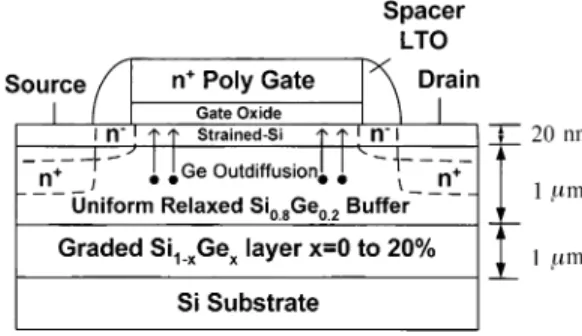
The schematic structure of the strained-Si nMOSFET is illustrated in Fig. 1. The Si Ge graded buffer layer was expitaxially grown on a p-type Si substrate at 600 C. Silane and germane were used as the Si and Ge precursors, respec-tively, and the Ge content of the graded buffer increased
Manuscript received May 7, 2004. This work was supported by the National Science Council of Taiwan, R.O.C. under Contract 92-2215-E-002-007 and Contract 92-2120-E-002-006. The review of this letter was arranged by Editor T.–J.King.
W.-C. Hua, S. Maikap, and C. W. Liu are with the Department of Electrical Engineering, Graduate Institute of Electronics Engineering, National Taiwan University, Taipei, Taiwan, R.O.C. (e-mail: [email protected]).
M. H. Lee and P. S. Chen are with the Electronics Research and Service Organization, Industrial Technology Research Institute (ERSO/ITRI), Hsinchu 300, Taiwan, R.O.C.
K. M. Chen is with the National Nano Device Laboratories, Hsinchu 300, Taiwan, R.O.C.
Digital Object Identifier 10.1109/LED.2004.834884
Fig. 1. Schematic diagram of a strained-Si nMOSFET.
from 0% to 20% over the thickness of 1 m. A 1- m-thick relaxed Si Ge layer was grown on the graded buffer layer, and a 20-nm strained-Si layer was grown on the uniform re-laxed Si Ge layer. The surface roughness of the resulting strained-Si is nm after the device fabrication, measured by the atomic force microscope. All the epitaxial layers were prepared by the ultrahigh-vacuum chemical vapor deposition reactor. Both the strained-Si and the control Si nMOSFETs were fabricated by the same process with the 25- m gate width and the 0.8- m gate length. The maximum thermal budget is 960 C for 7 min. The tensile strain in the Si channel is %, measured by surface Raman spectroscopy [3]. The treading dislocation density on the strained-Si is cm , and almost no dislocation penetrates into the device with m and m. The effect of the threading dislocation can be neglected in these devices.
III. RESULTS ANDDISCUSSION
The normalized input referred gate voltage noises (NS for both the strained-Si and the control Si nMOSFETs with rapid thermal oxidation (RTO) (5 nm at 900 C for 5 min) and de-posited tetraethylorthosilicate (TEOS) oxide (30 nm at 700 C for 1 h) are shown in Fig. 2. NS is independent of oxide thick-ness and is given by
NS (1)
where is the input referred gate voltage noise, is the drain current noise, is the transconductance, , and are the dielectric constant and thickness of the gate oxide, respec-tively. is the equivalent oxide traps per unit area, and are channel width and length, respectively, and is frequency. Equation (1) is based on the carrier number fluctuation model [4]–[6] also known as the trapping-detrapping model originated by McWhoter [4], [5] for the nMOSFET. The effect of the oxide thickness on the flicker noise can be normalized in (1). All the
694 IEEE ELECTRON DEVICE LETTERS, VOL. 25, NO. 10, OCTOBER 2004
Fig. 2. NS of the strained-Si and the control Si devices with RTO and TEOS oxide. The strained-Si device with RTO gate oxide has a much higher NS than the control device with RTO, but the strained-Si device with TEOS gate oxide shows slightly increased NS than the control device.
Fig. 3. D of the strained-Si and control Si devices with TEOS and RTO oxide. The strained-Si device with RTO oxide has the highestD of 5 2 10 eV cm due to the oxidation-enhanced Ge outdiffusion.
devices are biased at triode region with the same (60 A) and very small (0.05 V) to maintain the similar condition as the extraction measurement (no lateral electric field in the channel). Even though the four devices are biased at different ef-fective gate voltages NS is still comparable since the
is normalized to the square of the transconductance ( dependence). Note that is only weakly dependent on the gate voltage when [6]. The measured transconduc-tance is used in the NS calculation. Fig. 2 shows that for RTO gate oxide, the strained-Si MOSFET yields a higher NS than the control device at the same frequency, but for the TEOS gate oxide, the strained-Si MOSFET exhibits only a slightly higher NS than the control one. The results can be explained by the carrier number fluctuation theory and the Ge outdiffusion [7]. Since the NS is proportional to the in (1) and the is approximately proportional to the interface trap densities , the NS can be directly related to the . The of the four devices can be obtained from the high-low frequency capacitance–voltage (C–V) (Fig. 3) [8]. The order of the NS level in Fig. 2 is consistent with the level in Fig. 3. For the control Si devices, the RTO device has lower and NS as compared to the TEOS device due to the high quality thermal oxide formation at 900 C. However, the strained-Si device with RTO oxide has the highest and NS due to the oxida-tion-enhanced Ge outdiffusion. At the high temperature RTO process, the Si-interstitials at Si/oxide interface were injected
Fig. 4. Room temperature quasi-static C–V curves of strained-Si devices with TEOS and RTO oxide.
into the underneath Si–SiGe heterojunction, and the interstitials enhanced the Ge outdiffusion in the relaxed SiGe layer into the strained-Si/oxide interface. The Ge acts as a trap center. The traps near the strained-Si/oxide interface enhance the random trapping and detrapping processes of charges. The charge fluc-tuation induces the flucfluc-tuation of the surface potential and mod-ulates the channel carrier density. As a result, the flicker noise of the strained-Si device with RTO oxide increases. The satu-ration drain current of the strained-Si device has a 35% increase and a % decrease at V as compared to the control device for TEOS and RTO oxides, respectively. The decrease of of the strained-Si device with RTO oxide as compared to the control device with the same RTO oxide also suggests that Ge traps can decrease the electron mobility. The mobility enhancement obtained by low temperature process has been reported previously [9]. Both the NS and are sim-ilar for the strained-Si and control Si devices with low temper-ature TEOS oxide. This indicates that for the low tempertemper-ature (TEOS) process, the Ge outdiffusion at 700 C is not significant and the interface trap densities are almost similar for both the strained-Si and the control Si devices. Note that the Ge diffusion at 950 C without Si-interstitial injection can be enhanced for strained-Si [10]. This may be responsible for the slightly higher NS and of the strained-Si device with TEOS oxide as compared to the control Si device with the same TEOS oxide.
To further confirm the Ge outdiffusion, quasi-static (C–V) measurements of strained-Si devices with the TEOS and RTO oxide at room temperature are performed (Fig. 4). For the strained-Si device with TEOS gate oxide, the hole confinement shoulder due to the strained-Si/relaxed SiGe heterojunction [11] is clearly observed in the C–V curves at the accumulation region ( V). The existence of the hole confinement shoulder is confirmed by quasi-static C–V measurements from room temperature to 230 C. However, for the strained-Si de-vice with RTO gate oxide, no such hole confinement shoulder is observed. This indicates that the strained-Si/relaxed SiGe heterojunction of the RTO device is smeared out due to the Ge outdiffusion during the RTO process.
IV. CONCLUSION
Both the disappearance of hole confinement shoulder in the
C–V measurements and the increase of and NS for the strained-Si device with RTO oxide indicate the Ge outdiffu-sion from the Si–SiGe heterojunction which smears out the
HUA et al.: Ge OUTDIFFUSION EFFECT ON FLICKER NOISE IN STRAINED-Si nMOSFETs 695
abruptness of the heterojunction, and forms interface traps at the Si/oxide interface. The low temperature oxide is required to avoid the injection of Si-interstitials and the Ge outdiffusion.
REFERENCES
[1] J. L. Hoyt, H. M. Nayfeh, S. Eguchi, I. Aberg, G. Xia, T. Drake, E. A. Fitzgerald, and D. A. Antoniadis, “Strained silicon MOSFET tech-nology,” in IEDM Tech. Dig., 2002, pp. 23–26.
[2] K. Rim, S. Narasimha, M. Longstreet, A. Mocuta, and J. Cai, “Low field mobility characteristics of sub-100 nm unstrained and strained Si MOS-FETs,” in IEDM Tech. Dig., 2002, pp. 43–46.
[3] J. C. Tsang, P. M. Mooney, F. Dacol, and J. O. Chu, “Measurements of alloy composition and strain in thin Ge Si layers,” J. Appl. Phys., vol. 75, no. 12, pp. 8098–8108, 1994.
[4] A. L. McWhorter, “Semiconductor surface physics,” Ph.D. dissertation, Lincoln Lab., Mass. Inst. Technol., Lexington, MA, 1955.
[5] A. L. McWhorter, Semiconductor Surface Physics, R. H. Kinston, Ed. Philadelphia, PA: Univ. Penn., 1957.
[6] Y. Nemirovsky, I. Brouk, and C. G. Jakobson, “1=f noise in CMOS transistors for analog applications,” IEEE Trans. Electron. Devices, vol. 48, pp. 921–927, May 2001.
[7] P. Fahey, S. S. Lyer, and G. J. Scilla, “Experimental evidence of both interstitial- and vacancy-assisted diffusion of Ge in Si,” Appl. Phys. Lett., vol. 54, no. 9, pp. 843–845, 1989.
[8] E. H. Nicollian and J. R. Brews, MOS (Metal Oxide Semiconductor) Physics and Technology. New York: Wiley, 1991.
[9] K. Rim, J. L. Hoyt, and F. Gibbons, “Fabrication and analysis of deep submicron strained-Si N-MOSFETs,” IEEE Trans. Electron Devices, vol. 47, pp. 1406–1415, July 2000.
[10] T. Mizuno, N. Sugiyama, T. Tezuka, T. Numata, T. Maeda, and S. Takagi, “Design for scaled thin film strained-SOI CMOS devices with higher carrier mobility,” in IEDM Tech. Dig., 2002, pp. 31–34.
[11] G. A. Armstrong and C. K. Majti, “Strained-Si channel heterojunction PMOSFETs,” Solid State Electron., vol. 42, no. 4, pp. 487–498, 1998.