The study of electrical characteristics of heterojunction based on ZnO
nanowires using ultrahigh-vacuum conducting atomic force microscopy
J. H. Hea兲and C. H. Ho
Institute of Photonics and Optoelectronics and Department of Electrical Engineering, National Taiwan University, Taipei, 106 Taiwan, Republic of China
共Received 30 August 2007; accepted 15 November 2007; published online 5 December 2007兲 The electrical performances of the heterojunction of n-ZnO nanowires with p-Si substrate at the nanometer scale have been characterized using an ultrahigh-vacuum conducting atomic force microscopy. Compared with the expected values of 1.0–2.0 reported in p-n junction in the previous studies, the abnormally high diode ideality factor共Ⰷ2兲 was obtained. It elucidates that a ZnO–Si p-n junction can be modeled by a series of diodes, the actual ZnO–Si junction diode and two Schottky diodes at the metal/ZnO and metal/Si junctions. The tunneling across p-n junction would also play a role in the externally measured high ideality factor. © 2007 American Institute of Physics. 关DOI:10.1063/1.2821831兴
ZnO-based materials and devices have attracted substan-tial interest since ZnO has several potensubstan-tial advantages, such as the commercial availability of bulk single crystals, wide band gap, and the large exciton binding energy共⬃60 meV compared to⬃25 meV for GaN兲.1The fabrication of effec-tive ZnO p-n homojunction remains to be accomplished since ZnO is intrinsically n-type materials, and the growth of reproducible high-quality p-type ZnO is not achieved yet. As an alternative way, ZnO-based heterojunctions are being in-vestigated for realizing device application.2–4In addition, the nanodevices based on ZnO nanowires共NWs兲, such as opti-cally pumped nanolaser,5 nanogenerator,6 acoustic resonator,7 piezoelectric gated diode,8field emitter,9 chemi-cal sensor,10and UV detector,11have been demonstrated due to the combination of structural, semiconducting, and piezo-electric properties of ZnO nanomaterials. Recently, the stud-ies of the NW-based heterojunctions, such as n-ZnO NWs/p-GaN 共Ref.12兲 and n-ZnO/p-Si,13,14have been fab-ricated to investigate their electrical and optoelectronic prop-erties, including the current-voltage 共I-V兲, electrolumines-cent, and photoresponse measurements. Therefore, it is essential to gain a better insight into the electrical properties of the p-n heterojunction diode above.
According to the Sah-Noyce-Shockley theory,15the for-ward current in a p-n junction is dominated by recombina-tion of minority carriers injected into the neutral regions of the junction. This kind of transport gives an ideality factor of 1.0. Recombination of carriers in the space-charge region, mediated by recombination centers located near the intrinsic Fermi level, results in an ideality factor of 2.0. However, the Sah-Noyce-Shockley model cannot account for ideality fac-tors greater than 2.0 found in p-n junction.
In the present study, we have demonstrated the electrical performances of a heterojuction of n-ZnO NW with p-Si at the nanoscale using ultrahigh-vacuum conducting atomic force microscopy共C-AFM兲. To analyze measured electrical transport, we propose an explanation for the high ideality factor in ZnO–Si heterojunciton. It elucidates that a ZnO–Si p-n junction can be modeled by a series of diodes, the actual ZnO–Si junction diode and two Schottky diodes at the metal/
ZnO and metal/Si junctions. A theoretical model on the ef-fective ideality factor of a system of junctions is in agree-ment with the experiagree-mental data.
Fabrication of heterojunction n-ZnO/p-Si has been re-ported elsewhere.13 Electrical measurements of heterojuc-tions of ZnO NWs/p-Si substrate were made using a stan-dard commercial instrument 共Omicron ultrahigh-vacuum variable temperature AFM兲. The pressure in the analysis chamber was below 5⫻10−11mbar during the experiments.
C-AFM measurements were carried out in contact mode us-ing silicon cantilevers with constant loadus-ing forces in the range between 30 and 50 nN. The AFM tip was precoated with a PtIr layer, provided by the manufacturer 共Nanosen-sors兲, and subsequently coated with a Ti/Au 共30 nm/30 nm兲 film by electron beam evaporation for obtaining Ohmic con-tact between Ti and ZnO. The 30-nm-thick Pt was also sput-tered onto the back side of the p-type Si substrate to obtain Ohmic contact. C-AFM tip is used to apply voltage and mea-sure the current through the NW and Si substrate.
Under controlled experimental condition, ZnO NW ar-rays were grown on Al2O3共11–20兲 substrate surface using
Au as catalyst. The phase of NWs is hexagonal wurtzite-structured ZnO, and the growth direction of ZnO NW arrays is关0001兴 direction.16
An undoped ZnO NW usually exhibits n-type character-istics due to presence of zinc interstitials and/or oxygen va-cancies. The I-V curves analyzed by two-electrode transport measurement for a ZnO NW deposited on an insulating layer and connected by a pair of Ti/Au electrodes as an Ohmic metal electrode, and a boron-doped Si substrate connected by a pair of Pt electrodes as an Ohmic electrode for p-type Si indicate that the linear trend shows the establishment of Ohmic contacts, as shown in Fig.1. The detailed method to deposit metal electrodes onto a NW has been reported elsewhere.17 After ensuring Ohmic characteristics for the metal-semiconductor interface, I-V characteristics of the Si/ZnO heterojunction could be measured further. After fab-ricating heterojunction based on ZnO NWs, electrical mea-surements were performed in C-AFM. The C-AFM probe was positioned directly onto the NW and used to apply volt-age and measure the current through the NW and Si sub-strate, as shown in Fig.2共a兲. Previous study indicates good a兲Electronic mail: [email protected].
APPLIED PHYSICS LETTERS 91, 233105共2007兲
0003-6951/2007/91共23兲/233105/3/$23.00 91, 233105-1 © 2007 American Institute of Physics
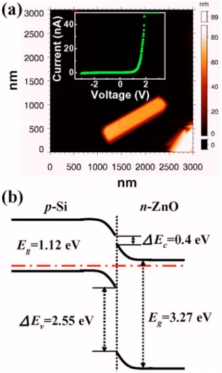
contact between the ZnO NWs and Si substrate and unifor-mity in electrical performance along ZnO NW.13The inset of Fig. 2共a兲 shows that a pronounced rectifying diodelike be-havior was observed, while the AFM tip was used to contact the ZnO NW and to apply voltage. An energy band diagram is drawn in Fig.2共b兲based on individual band structures to explain the behavior of n-ZnO/p-Si heterojunction. It is known that the energy gaps共Eg兲 for ZnO and Si are 3.27 and
1.12 eV, respectively. The valence band offset is much larger than the conduction band offset. The higher barrier in the valence band prevents the holes’ movement. Therefore, the conductive property of this heterojunction is determined by the electrons in the conduction band. However, these argu-ments are for the ideal case, and direct measureargu-ments are required to determine the exact band structure of the hetero-junction.
The ideality of the diode can be determined from the forward-biased characteristic. Figure 3 is a semilogarithmic plot of current versus forward bias of the inset of Fig.2共a兲. The forward-biased current is
I = IS
冋
exp冉
eV nkT冊
− 1册
, 共1兲 n = e kT dV d ln I, 共2兲where n is the ideality factor which is a quantity for describ-ing the deviation of the diode from an ideal p-n junction, for which n = 1, IS is the reverse saturation current, V is the
forward-biased voltage, k is the Boltzmann constant, and T is the absolute temperature. Fitting of the experimental data using Eq. 共1兲 yields n values. The values of n obtained for the p-Si/n-ZnO heterojunction were found to be approxi-mately 4.28 at voltages ranging from 0.46 to 0.85 V and ap-proximately 9.44 at voltages ranging from 0.85 to 1.89 V. According to the Sah-Noyce-Shockley theory,15the values of the ideality factor are around 1.0 at a low voltage and up to 2.0 at a higher voltage. However, the theoretical model can-not account for ideality factors greater than 2.0 found in the present study. This can be attributed to the presence of non-linear metal-semiconductor contact.18–20 The heterojunction diode can then be modeled by a series connection of diodes or resistances in a dissimilar bias range: the actual p-type Si/n-type ZnO heterojunction diode, the contact resistance between metal/p-type Si共or Schottky diode兲, and the contact resistance between metal/n-type ZnO 共or Schottky diode兲. Although the two metal-semiconductor junctions of a diode ideally have Ohmic characteristics, the contacts could exhibit nonlinear characteristics in the interim bias voltage range. As forward bias just applied, it is p-type Si/n-type ZnO hetero-junction diode with two ideal metal-semiconductor contact
FIG. 1.共Color online兲 I-V characteristics of the ZnO NW with Ti/Au con-tacts and Si with the Pt concon-tacts showing Ohmic characteristics.
FIG. 2. 共Color online兲 共a兲 AFM topography image of heterojunction diode based on ZnO nanowires共inset: electron transport characteristics of ZnO/Si heterojunction兲. 共b兲 The energy band diagram of the heterojunction
n-ZnO/p-Si at zero voltage bias.
FIG. 3.共Color online兲 A logarithm plot of current vs bias in the inset of 共b兲. The curve can be simulated with diode ideality factors n = 4.28 in the range from 0.46 to 0.85 V and n = 9.44 in the range from 0.85 to 1.89 V.
233105-2 J. H. He and C. H. Ho Appl. Phys. Lett. 91, 233105共2007兲
resistances. In the limit of high contact resistance, the metal-semiconductor contact could be considered as reverse-biased Schottky contact in the interim bias voltage range.21 There-fore, it could be a p-Si/n-ZnO heterojunction, metal/p-type Si Schottky diode, and/or metal/n-type ZnO Schottky diode in the interim bias voltage range 共⬍1.89 V兲. These three diodes have different values of reverse saturation current and ideality factors. A summation of three diodes could be used to model the various conduction mechanisms. As the external current and voltage are given by I and V =兺Vi, the I-V
char-acteristic of the structure is given by V =
兺
i Vi=兺
i冋
ni冉
kT e冊
ln I − ni冉
kT e冊
ln ISi册
, 共3兲 where the factor ISiis the reverse saturation current of eachjunction, Vi is the voltage at each junction, and ni is the
ideality factor of each junction. We assume that the diode voltages are ViⰇkT/e, so that exp共eV/nkT兲Ⰷ1.
Rearrange-ment of the terms in the above equation yields ln I =共e/kT兲
兺ini
V +兺iniln ISi 兺ini
. 共4兲
In Eq.共4兲, the second summation is a constant, since we consider only the linear region of the ln共I兲-V characteristic, where ni are constants. According to Eq.共4兲, the externally
measured ideality factor is a sum of the ideality factors of the individual rectifying junctions. This result can be expressed as n =兺ini, where ni represent the ideality factors of
p-Si/n-ZnO heterojunction, metal/p-type Si junction, and metal/n-type ZnO junction. Accordingly, it is evident that the ideality factor of the diodeⰇ2 can be measured. In addition, since two metal-semiconductor contacts 共metal/ZnO and metal/Si兲 could be turned into reverse-biased Schottky con-tact at different bias voltages, two slopes, which stands for two n values, were obtained at bias voltages ranging from 0.46 to 1.89 V. As shown in Fig.3, in the bias voltage range greater than 1.89 V, the equivalent circuit of the device turns out to be three resistances instead of the combination of p-Si/n-ZnO heterojunction, metal/p-type Si Schottky diode, and metal/n-type ZnO Schottky diode, since the I-V charac-teristic in the inset of Fig.2共a兲is linear when bias voltage is higher than 1.89 V.
Moreover, the high ideality factors 共nⰇ2.0兲 in GaN-based light-emitting diodes22,23were attributed to deep-level-assisted tunneling24 across p-n junction, since the measure-ment of the I-V behavior demonstrated a temperature independent semilogarithmic slope, which is characteristic of deep-level-assisted tunneling current rather than diffusion or space-charge recombination current where the ideality factor n varies between 1.0 and 2.0. Therefore, in addition to the sum of the ideality factors of the individual rectifying junc-tions 共i.e., the actual ZnO–Si junction diode and two Schottky diodes at the metal/ZnO and metal/Si junctions兲,
the tunneling across p-n junction would also play a role in the externally measured high ideality factor in this study.
In summary, we have demonstrated the electrical perfor-mances of a heterojuction of n-ZnO NW with p-Si substrate at the nanoscale using C-AFM. To gain a better understand-ing of the measured electrical properties of the p-n hetero-junction diode above, the theoretical model was proposed to analyze the anomalously high ideality factor of the prepared p-n junction diode. The externally measured ideality factor of Si/ZnO diode is the sum of the ideality factors of the individual rectifying junction. The tunneling across Si/ZnO p-n junction would also play a role in the externally mea-sured high ideality factor.
The research was supported by the National Science Council under Grant No. NSC 96-2112-M-002-038-MY3 and NSC 96-2622-M-002-002-CC3.
1U. Ozgur, Y. I. Alivov, C. Liu, A. Teke, M. A. Reshchikov, S. Dogan, V. Avrutin, S. J. Cho, and H. Morkoc, J. Appl. Phys. 98, 041301共2005兲. 2I. S. Jeong, J. H. Kim, and S. Im, Appl. Phys. Lett. 83, 2946共2003兲. 3J. D. Ye, S. L. Gu, S. M. Zhu, W. Liu, S. M. Liu, R. Zhang, Y. Shi, and
Y. D. Zheng, Appl. Phys. Lett. 88, 182112共2006兲.
4Y. I. Alivov, Ü. Özgür, S. Dogan, D. Johnstone, V. Avrutin, N. Onojima, C. Liu, J. Xie, Q. Fan, and H. Morkoç, Appl. Phys. Lett. 86, 241108 共2005兲.
5M. H. Huang, S. Mao, H. Feick, H. Q. Yan, Y. Y. Wu, H. Kind, E. Weber, R. Russo, and P. D. Yang, Science 292, 1897共2001兲.
6Z. L. Wang and J. H. Song, Science 312, 242共2006兲.
7B. A. Buchine, W. L. Hughes, F. L. Degertekin, and Z. L. Wang, Nano Lett. 6, 1155共2006兲.
8J. H. He, C. L. Hsin, J. Liu, L. J. Chen, and Z. L. Wang, Adv. Mater. 共Weinheim, Ger.兲 19, 781 共2007兲.
9Y. B. Li, Y. Bando, and D. Golberg, Appl. Phys. Lett. 84, 3603共2004兲. 10Z. Y. Fan, D. W. Wang, P. C. Chang, W. Y. Tseng, and J. G. Lu,
Appl. Phys. Lett. 85, 5923共2004兲.
11J. H. He, Y. H. Lin, M. E. McConney, V. V. Tsukruk, Z. L. Wang, and G. Bao, J. Appl. Phys. 102, 084303共2007兲.
12W. I. Park and G. C. Yi, Adv. Mater.共Weinheim, Ger.兲 16, 87 共2004兲. 13J. H. He, S. T. Ho, T. B. Wu, L. J. Chen, and Z. L. Wang, Chem. Phys.
Lett. 435, 119共2007兲.
14R. Ghosh and D. Basaka, Appl. Phys. Lett. 90, 243106共2007兲. 15C. Sah, R. N. Noyce, and W. Shockley, Proc. IRE 45, 1228共1957兲. 16H. He, C. S. Lao, L. J. Chen, D. Davidovic, and Z. L. Wang, J. Am. Chem.
Soc. 127, 16376共2005兲.
17C. L. Hsin, J. H. He, C. Y. Lee, W. W. Wu, P. H. Yeh, L. J. Chen, and Z. L. Wang, Nano Lett. 7, 1799共2007兲.
18C. X. Wang, G. W. Yang, H. W. Liu, Y. H. Han, J. F. Luo, C. X. Gao, and G. T. Zou, Appl. Phys. Lett. 84, 2427共2004兲.
19J. M. Shah, Y. L. Li, T. Gessmann, and E. F. Schubert, J. Appl. Phys. 94, 2627共2003兲.
20C. X. Wang, G. W. Yang, T. C. Zhang, H. W. Liu, Y. H. Han, J. F. Luo, C. X. Gao, and G. T. Zou, Diamond Relat. Mater. 12, 1548共2003兲. 21J. C. Ranuarez, F. J. G. Sanchez, and A. Ortiz-Conde, Solid-State Electron.
43, 2129共1999兲.
22H. C. Casey, Jr., J. Muth, S. Krishnankutty, and J. M. Zavada, Appl. Phys. Lett. 68, 2867共1996兲.
23P. Perlin, M. Osinski, P. G. Eliseev, V. A. Smagley, J. Mu, M. Banas, and P. Sartori, Appl. Phys. Lett. 69, 1680共1996兲.
24D. J. Dumin and G. L. Pearson, J. Appl. Phys. 36, 3418共1965兲.
233105-3 J. H. He and C. H. Ho Appl. Phys. Lett. 91, 233105共2007兲