IEEE TRANSACTIONS ON CIRCUITS AND SYSTEMS—I: REGULAR PAPERS, VOL. 54, NO. 4, APRIL 2007 807
Design of an FFT/IFFT Processor for
MIMO OFDM Systems
Yu-Wei Lin and Chen-Yi Lee, Member, IEEE
Abstract—In this paper, we present a novel 128/64 point fast
Fourier transform (FFT)/ inverse FFT (IFFT) processor for the applications in a multiple-input multiple-output orthogonal fre-quency-division multiplexing based IEEE 802.11n wireless local area network baseband processor. The unfolding mixed-radix multipath delay feedback FFT architecture is proposed to effi-ciently deal with multiple data sequences. The proposed processor not only supports the operation of FFT/IFFT in 128 points and 64 points but can also provide different throughput rates for 1–4 simultaneous data sequences to meet IEEE 802.11n requirements. Furthermore, less hardware complexity is needed in our design compared with traditional four-parallel approach. The proposed FFT/IFFT processor is designed in a 0.13- m single-poly and eight-metal CMOS process. The core area is 660 2142 m2, including an FFT/IFFT processor and a test module. At the oper-ation clock rate of 40 MHz, our proposed processor can calculate 128-point FFT with four independent data sequences within 3.2
s meeting IEEE 802.11n standard requirements.
Index Terms—80211n, fast Fourier transform (FFT),
mul-tiple-input multiple-output (MIMO) orthogonal frequency-divi-sion multiplexing (OFDM).
I. INTRODUCTION
T
HE combination of the multiple-input multiple-output (MIMO) signal processing with orthogonal frequency-di-vision multiplexing (OFDM) communication system is con-sidered as a promising solution for enhancing the data rates of the next generation wireless communication systems oper-ating in frequency-selective fading environments. The High Throughput Task Group which establishes IEEE 802.11n standard is going to draw up the next-generation wireless local area network (WLAN) proposal based on the 802.11 a/g which is the current OFDM-based WLAN standards [1]. The IEEE 802.11n standard based on the MIMO OFDM system provides very high data throughput rate from the original data rate 54 Mb/s to the data rate in excess of 600 Mb/s because the technique of the MIMO can increase the data rate by extending an OFDM-based system. However, the IEEE 802.11n standard also increases the computational and the hardware complexities greatly, compared with the current WLAN standards. It is a challenge to realize the physical layer of the MIMO OFDM system with minimal hardware complexity and power con-Manuscript received August 23, 2005; revised June 21, 2006. This work was supported by NSC under Grant NSC-94–2215–E-009–044 and by MOEA under Grant 95-EC-17-A-01–S1031. This paper was recommended by Associate Ed-itor P. Nilsson.Y.-W. Lin is with the MediaTek Inc., HsinChu 300, Taiwan, R.O.C. (e-mail: YW_Lin@mtk.com.tw).
C.-Y. Lee is with the Department of Electronics Engineering, National Chiao Tung University, HsinChu 300, Taiwan, R.O.C. (e-mail: cylee@si2lab.org).
Digital Object Identifier 10.1109/TCSI.2006.888664
sumption—especially the computational complexity—in VLSI implementation. The FFT/IFFT processor is one of the highest computational complexity modules in the physical layer of the IEEE 802.11n standard. According to IEEE 802.11n standard, the execution time of 128-point and 64-point with 1–4 simul-taneous data sequences must be calculated within 3.6 or 4.0 s. Therefore, if employing the traditional approach to solve the simultaneous multiple data sequences, several FFT/IFFT processors are needed in the physical layer of a MIMO OFDM system. Thus, the hardware complexity of the physical layer in a MIMO OFDM system will be very high. This paper proposes an FFT/IFFT processor with a novel multipath pipelined archi-tecture to deal with the issue of the multiple data sequences for MIMO OFDM applications. The 128/64-point FFT/IFFT with 1–4 simultaneous data sequences can be supported in our proposed processor with minimal hardware complexity. Fur-thermore, the power consumption can also be saved by using higher radix FFT algorithm. The paper is organized as follows. Section II describes the problems of the implementation of the FFT/IFFT processor in a MIMO OFDM system. The 128-point mixed-radix FFT algorithm including radix-2 FFT algorithm and three-step radix-8 FFT algorithm, the 64-point three-step radix-8 FFT algorithm and the IFFT algorithm is described in Section III. Section IV focuses on describing the proposed FFT/IFFT architecture for IEEE 802.11n applications. In Section V, the layout view of the proposed FFT/IFFT processor and the simulation results are presented. Then, conclusions are drawn in Section VI.
II. DESIGN ISSUE OF FFT PROCESSOR FOR MIMO OFDM SYSTEM
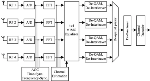
A block diagram of the receiver of IEEE 802.11n standard is shown in Fig. 1. It contains four RFs, four analog-to-digital con-verters (ADCs), four FFTs, a MIMO equalizer, four de-qam and interleaver, a spatial parser, a puncturer, a channel de-coder, a synchronization block, and a channel estimation block. Depending on the desired data rate, the modulation scheme can be binary phase shift keying (BPSK), quaternary phase shift keying (QPSK), or quadrature amplitude modulation (QAM) with 1–6 bits. The encoding rates in this specification are 1/2, 2/3, 3/4, or 7/8. The number of spatial sequence is supported by 1, 2, 3, or 4. The guard interval period is 400 ns or 800 ns. The bandwidth of the transmitted signal is 20 or 40 MHz. The FFT size is 64 points or 128 points. Thus, the FFT/IFFT processor has to calculate 128 points or 64 points with simultaneous 1–4 data sequences within 3.6 or 4 s depending on the number of spatial sequence, the guard interval and the FFT size.
In the last three decades, various FFT architectures, such as single-memory architecture, dual-memory architecture 1549-8328/$25.00 © 2007 IEEE
Fig. 1. Block diagram of the receiver of IEEE 802.11n standard.
[2], pipelined architecture [3], array architecture [4], and cached-memory architecture [5], have been proposed. How-ever, to our knowledge, few papers have reported how to deal with multiple data sequences based on these FFT architectures. In general, multiple FFT processors are added to deal with multiple data sequences in a MIMO OFDM system, as shown in Fig. 1, and therefore cause a large increase in the hardware complexity and power consumption, compared with that of the single FFT processor. In addition, the throughput rate of the FFT processor for the high-speed WLAN applications is very high. A good FFT processor should not only provide a high throughput rate, but also deal with multiple data se-quences effectively for MIMO OFDM applications. In our view, the pipelined architecture should be the best choice for the high throughput rate applications since it can provide high throughput rate with acceptable hardware cost. The pipelined FFT architecture typically falls into one of the two following categories. One is multipath delay commutator (MDC) and the other is single-path delay feedback (SDF) [3]. In general, the MDC scheme can achieve higher throughput rate by using mul-tiple data paths, while the SDF scheme needs less memory and hardware complexity with the delay feedback scheme. Besides, the operation of the complex multiplication consumes lots of power in the FFT processor. In order to save power dissipation, higher radix FFT algorithm can be used to reduce the number of complex multiplications [6]. Three-step radix-8 FFT algorithm is chosen in our design to save complex multiplications. Be-cause 128-point FFT is not a power of 8, the mixed-radix FFT algorithm combining two different FFT algorithms is needed. The mixed-radix multipath delay feedback (MRMDF) FFT architecture can provide higher throughput rate with minimal hardware cost by combining the features of MDC and SDF [7]. However, this scheme can not deal with multiple input data sequences. The main motivation of this paper is to design a novel unfolding MRMDF structure based FFT processor for MIMO OFDM applications. In our proposed processor, the FFT architecture can not only deal with 1–4 simultaneous data sequences for MIMO OFDM applications but also save lots of hardware complexity, compared with the traditional approach as shown in Fig. 1.
ALGORITHM
Given a sequence , an -point discrete fourier transform (DFT) is defined as
(1) Where and are complex numbers. The twiddle factor is
(2) In (1), the computational complexity is through directly performing the required computation. By using the FFT algorithm, the computational complexity can be reduced to , where means the FFT. The radix-FFT algorithm can be easily derived from DFT by decomposing the -point DFT into a set of recursively related -point FFT transform, if is a power of . Higher radix FFT algorithm has less number of the nontrivial complex multiplications, compared with the radix-2 FFT algorithm which is the simplest form in all FFT algorithms [6]. In an example for 128-point FFT and 64-point FFT, the number of nontrivial complex multiplications of radix-8 FFT algorithm is 152 and 48, which is only 58.9%and 48.9% of that of radix-2 FFT algorithm [6]. Thus, in order to save power dissipation of the complex mul-tiplier operation, we choose radix-8 FFT algorithm to reduce the number of nontrivial complex multiplications. Because 128-point FFT is not a power of 8, the mixed-radix FFT algo-rithm, including radix-2 and radix-8 FFT algoalgo-rithm, is needed. Since the algorithm has been derived in detail previously [7], it will be described briefly here.
First let
LIN AND LEE: DESIGN OF FFT/IFFT PROCESSOR 809
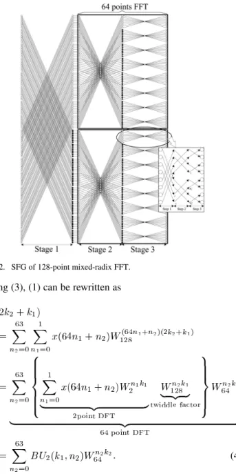
Fig. 2. SFG of 128-point mixed-radix FFT. Using (3), (1) can be rewritten as
(4) Equation (4) can be considered as a two-dimensional DFT. One is 64-point DFT and the other is 2-point DFT. Then, by de-composing the 64-point DFT into the 8-point DFT recursively 2 times, we can complete the 128-point mixed-radix FFT al-gorithm. In order to implement a radix-8 FFT algorithm more efficiently, using the radix- FFT algorithm [3], we further de-compose the butterfly of radix-8 FFT algorithm into three steps and apply the radix-2 index map to the radix-8 butterfly. The three-step radix-8 FFT was derived in detail in [7]. Fig. 2 shows the signal flow graph (SFG) of the 128-point mixed-radix FFT algorithm and two 64-point three-step radix-8 FFT algorithms. In Fig. 2, there are three stages in 128-point FFT algorithm. The radix-2 FFT algorithm is used in the first stage, and the radix-8 algorithm is applied in the second and third stages. And the but-terfly of radix-8 in stage 2 and stage 3 can be further decom-posed into three steps by using the radix- FFT algorithm. The
twiddle factors, and , at
the third step in each radix-8 butterfly are trivial complex mul-tiplications because they can be written as and , respectively. Thus, a complex multiplication
with one of the two coefficients can be computed using addi-tions and a real multiplication, whose hardware can be realized by six shifters and four adders [8]. The black point shown in Fig. 2 means that the specific twiddle factor will be multiplied at that point. Stage 2 and stage 3 can be considered as two 64-point radix-8 FFT algorithms. Therefore, if some data path and con-trol mode are added in 128-point FFT processor, the processor can also calculate 64-point FFT efficiently.
The IFFT of an -point sequence , is defined as
(5) In order to implement the IFFT algorithm more efficiently, (5) can be written as [7]
(6) According to (6), the IFFT can be performed by taking the com-plex conjugate of the incoming data first and then the outgoing data without changing any coefficients in the original FFT algo-rithm so that the hardware implementation can be more efficient.
III. ARCHITECTURE
A. Proposed FFT Architecture for a MIMO OFDM System
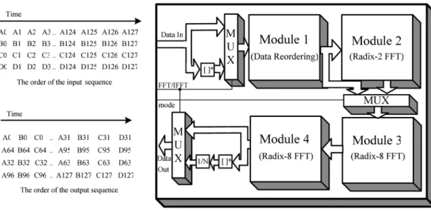
According to (4), (6), and SFG (Fig. 2), we propose a novel 128/64-point FFT/IFFT processor to support 1–4 simultaneous data sequences for a MIMO OFDM system, as shown in Fig. 3. The proposed FFT architecture combining the features of the SDF and MDC architectures consists of Module 1, Module 2, Module 3, Module 4, conjugate blocks, a division block, and multiplexers. The features of the proposed FFT architecture are as follows. First, 128- and 64-point FFT with 1–4 simultaneous data sequences can be operated in our design. Second, the pro-posed FFT architecture can provide several throughput rates to achieve the requirements of IEEE 802.11n standard. Third, the minimal memory is needed by using the delay feed back scheme to reorder the input data and the intermediate results of each module; the hardware complexity of the complex multipliers can be reduced by using the scheduling approach and the speci-fied constant multipliers; so the proposed FFT processor has less hardware complexity, compared with the approach using mul-tiFFT processors. And last, higher radix FFT algorithm can be implemented to save power dissipation regardless of the opera-tion of 64-point or 128-point FFT.
The order of the input sequences and output sequences has the specified order in the proposed FFT architecture. In Fig. 3, the letters, A, B, C, D, mean the different input sequences. The index means the number of FFT points. The index is from 0 to 127 and 0 to 63 for 128- and 64-point FFT, respectively. Because the order of input sequences, shown in Fig. 3 is the same as that of the data sequences from the ADC, shown in Fig. 1, no extra memory is required to reorder these input sequences before they are loaded into the FFT processor. In general, the order of the
Fig. 3. Block diagram of the proposed 128/64-pointFFT/IFFT processor.
Fig. 4. Relation between the input order and the output order of data in a se-quence.
output sequences is different from that of the input sequences in the pipelined FFT architecture. And the order of the output se-quences is usually dependent on the FFT algorithm, the number of data path, and the FFT architecture. In our design, the order among these four output sequences is the repetition of the order A, B, C, and D, as shown in Fig. 3. And the relationship of the input and output order of data in each data sequence is shown in Fig. 4. The bit-reversal addressing concept is described in detail in [9]. The operation of FFT or IFFT is controlled by the con-trol signal, FFT/IFFT, as shown in Fig. 3. When an IFFT is per-formed in our processor, the complex conjugate of the input data is taken and they will be performed by the process in treating FFT. Then, the complex conjugate of the output data from FFT will be taken again, and will be divided by 128 or 64 depending on the operation of 128- or 64- point FFT. Because both 128 and 64 are power of 2, the operation of the division is imple-mented by shifting the decimal point location. The operation of 128- or 64- point FFT/IFFT is controlled by the control signal, mode. If the operation of 64-point FFT/IFFT is performed, the calculated data from Module 1 will skip Module 2 and go into Module 3 directly. The function of Module 1 is to reorder the data among these four data paths into a specific order to imple-ment the operation of FFT/IFFT with multiple data sequences more efficiently. Module 2 is to implement a radix-2 FFT
algo-rithm, corresponding to the first stage of SFG, as shown in Fig. 2. Module 3 and Module 4 are to realize three-step radix-8 FFT algorithm, corresponding to the second and third stages of the SFG, as displayed in Fig. 2. Two different schemes are adopted in Module 3 and Module 4 to implement three-step radix-8 FFT algorithm to minimize the memory requirement and to ensure the correction of the FFT output data.
1) Module 1: Module 1 contains several different-size delay
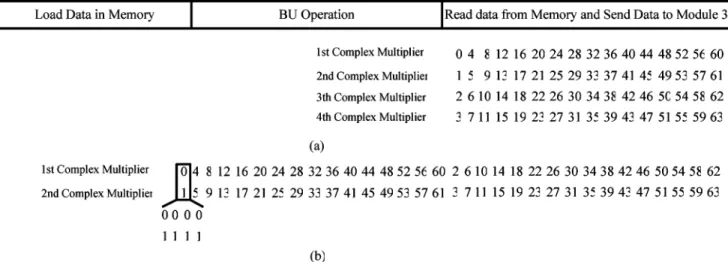
elements and a switch block, as in Fig. 5(a). The function of Module 1 is to reorder the input sequences to achieve two goals. One goal is to let Module 2, Module 3, and Module 4 implement the operation of FFT and IFFT with 1–4 simultaneous data quences more efficiently. The second goal is to avoid the data se-quences in Module 3 to be multiplied by the same twiddle factor in each data path simultaneously. Thus, the proposed complex multiplier can be used in Module 3 to reduce the hardware com-plexity by using the specified constant multipliers. The opera-tion of the Module 1 is shown in Fig. 5(b). First, the acopera-tion of the operation is to separate the four adjoining sequences by one delay unit. Then the separated data will be reordered among four sequences by the appropriate operation of the switch. Finally, the separated data will be adjusted by the delay elements, as shown in Fig. 5(b) [10]. The reordered data will be separated into 32 groups or 16 groups for 128- or 64-point, respectively. Each group contains four data sequences, A, B, C, and D. And each data sequence in the same group has the same FFT index, as shown in Fig. 5(b). In general, the operation of the FFT is data dependenT. For example, the FFT index 0 is operated with the FFT index 64 in the first stage of the 128-point mixed-radix FFT algorithm, as shown in Fig. 2. In order to implement the mul-tiple data sequences more efficiently, we separate the data into several groups. The group replacing the FFT index becomes the basic unit of the FFT operation. For example, group 0 is oper-ated with group 16 in the first stage of the 128-point mixed-radix FFT algorithm in our design. Because each data sequence in a group has the same FFT index, the operation of FFT/IFFT with multiple data sequences can be regarded as the duplication of the operation of one input sequence in the proposed FFT pro-cessor. In each group, the number of operations is decided by
LIN AND LEE: DESIGN OF FFT/IFFT PROCESSOR 811
Fig. 5. (a) Block diagram of Module 1. (b) Data scheduling and the operation of Module 1.
Fig. 6. Relation between the number of operation and the number of input se-quence in a group.
the number of data sequences. As seen in Fig. 6, if there is only one data sequence, the number of operations in the group is one; with two data sequences, the number of operations in the group becomes two and so on. Based on the data ordering and the con-cept of group in Module 1, the operation of FFT/IFFT with mul-tiple data sequences can be implemented more efficiently.
2) Module 2: In general, four complex multipliers are needed
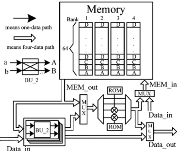
in the four-parallel approach to implement a radix-2 FFT algo-rithm. In this work, a group concept is used to deal with multiple data sequences and only two complex multipliers are used in this module. A block diagram of Module 2 consisting of a memory, 4 butterfly units of radix-2 FFT algorithm (BU_2), two com-plex multipliers, two ROMs, and some multicom-plexers is shown in Fig. 7. If 64-point FFT/IFFT is operated in our scheme, the data will skip this module. The memory size can store the data of 16 groups containing 256 complex data. Because four data paths are adopted in our design, four memory banks are needed to
Fig. 7. Block diagram of Module 2.
provide four data from memory to BU_2 simultaneously. Only 1/8 period of cosine and sine waveforms are stored in ROM and the other period waveforms can be reconstructed by these stored values. The operation of BU_2 is complex addition and com-plex subtraction from two input data. Because radix-2 FFT al-gorithm is adopted in this module, BU_2 can not start until both
input sequences and , when , are
available. This corresponds to the first stage of SFG, as shown in Fig. 2. According to the group data format, the data of the first 16 groups are stored in the memory. When the data of the next 16 groups enter Module 2, the eight input data are loaded into four BU_2s, four from the memory and four from the input,
Fig. 8. Scheduling of the twiddle factorW wherep is from 0 to 63. (a) Traditional four parallel architecture with four complex multipliers. (b) Our proposed unfolding approach with two complex multipliers.
Fig. 9. Block diagram of Module 3.
respectively. The operation of BU_2 in a group is dependent on the number of the data sequences. Four BU_2s generate eight output data according to radix-2 FFT algorithm; four output data will be fed to the Module 3 directly, while the other four output data will be stored in the memory. After the operation of BU_2, there are 16 groups fed to the Module 3 and 16 groups fed back to the memory. Then, these data stored in the memory are read and are multiplied by the twiddle factors simultaneously before they are sent to Module 3. The scheduling of the twiddle factor is shown in Fig. 8(a). In four-parallel approach, the utilization rate of the complex multiplier is only 50%. The proposed ap-proach can increase the utilization rate and reduce the number of complex multipliers [7]. The detailed operation is described below. Four output data must be generated after BU operation. Two of these four output data are multiplied by the appropriate twiddle factors first before they are stored in the memory; the other two are multiplied by the twiddle factors before they are fed to Module 3. The twiddle factor scheduling of the proposed approach is shown in Fig. 8(b). The data of each data path in the group are multiplied by the same twiddle factors. So the twiddle factor will be unfolded times, where is the number of the input data sequences. By rescheduling the timing of the com-plex multiplications, only two comcom-plex multipliers are needed and the utilization of the complex multipliers can achieve 100% in this scheme.
3) Module 3: Module 3 consists of three stages and one
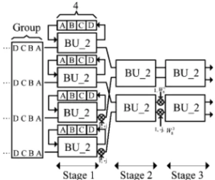
mod-ified complex multiplier, as shown in Fig. 9. The architecture of Module 3 is directly mapped from 3-step radix-8 FFT algorithm,
whose SFG is shown in Fig. 2. Four identical components are used in each stage since four-parallel approach is adopted. In our design, four input data are loaded into Module 3 from the previous module simultaneously. The different data sequences A, B, C, and D are considered as a group, as shown in Fig. 9. The size of the delay element in three stages is 32 (8 group), 16 (4 group) and eight (2 group), respectively, as shown in Fig. 9. The function of delay element is to store the input data until the other available input data is received for the BU_2 opera-tion. The operations of BU_2 of each stage, which is the same as that of BU_2 in Module 2 shown in Fig. 7, are the complex addition and the complex subtraction. For example, the data of the first 8 groups are stored in the delay elements in the first stage of Module 3. When the data of the next groups are valid from the input, eight data are fed to four BU_2s from both the input and the delay element. The output data generated by the BU_2 in the first stage or second stage are multiplied by a trivial twiddle factor, 1, or 1, ,
and ,
before they are fed to the next stage. These twiddle factors can be implemented efficiently, as mentioned in Section III. But the four output data from the third stage of Module 3 need to be multiplied by the nontrivial twiddle factors simultaneously in the modified complex multiplier. In the same group, the output data of each data path are multiplied by the same twiddle factors. It is inefficient to build four complex multipliers in four data paths for multiplying different twiddle factors simultaneously. So we use the proposed approach to reduce the complexity of
LIN AND LEE: DESIGN OF FFT/IFFT PROCESSOR 813
Fig. 10. Block diagram of Module 4.
the complex multipliers [7]. The twiddle factors of the
modi-fied complex multiplier are ,
where and are the
real and imaginary parts of the twiddle factor and p is from 0 to 49. In practice, only nine sets of constant values, ( , ) with to 8 are needed because the other twiddle factors can be obtained by using the trigonometric function. And these constant values can be realized more efficiently by using several adders and shifters. The detailed block diagram and function statement are described in [7]. The gate count of this approach can be saved about 38%, compared to four-complex-multiplier approach. And the performance of this approach is equivalent to that of the four complex multipliers.
4) Module 4: The block diagram of the Module 4 is shown in
Fig. 10. Three-step radix-8 FFT algorithm is realized in Module 4. This corresponds to the third stage of SFG, as shown in Fig. 2. There are also three stages in Module 4 to implement three-step radix-8 FFT algorithm, as shown in Fig. 10. The scheme of the Module 4 is different from that of Module 3 because the two available data of the BU_2 in the second stage and third stage are in the different data paths. So the structure of Module 4 is modified to ensure that the FFT output data are correct. Some output data generated by the BU_2 in the first stage and second stage are multiplied by the nontrivial twiddle factors before they are fed to the next stage.
B. Performance Analysis and Comparison
1) Performance Analysis: In IEEE 802.11n standard, the
128-point and 64-point FFT/IFFT are used for the bandwidth of 40 and 20 MHz, respectively. And 1–4 simultaneous data se-quences must be supported in this specification according to the number of antennas used. Eight operation modes of the FFT/ IFFT processor are needed in IEEE 802.11n standard, as listed in Table I. Two operation clock rates of our scheme, 40 and 20 MHz, are needed for the operation of 128-point and 64-point FFT/IFFT. The effective throughput rates of our design are de-pendent on the number of data sequences and can be calculated as
(7) where the operation ratio is defined as the number of data se-quences divided by 4. In general, while the number of data sequences is less than four, the number of operations is less than four in each group, as shown in Fig. 6. So the effective
TABLE I
PERFORMANCE OFOPERATIONMODES INOURPROPOSEDFFT ARCHITECTURE
throughput rate will be less than . For an example, if the number of data sequences is three, only three operations are needed in each group, as shown in Fig. 6. So the operation ratio is 3/4 and the effective throughput rate is equivalent to , using (7). Table I lists the effective throughput rates of our proposed FFT/IFFT processor in different operation modes. The effective throughput rate of each operation mode in our proposed FFT processor can meet the requirements of IEEE 802.11n, as seen in Table I.
2) Comparison: While the throughput rate of the pipelined
FFT architecture is increased by using the multiple data-path approach, the hardware cost of the FFT processor will be in-creased, too. Besides, the hardware costs are also strongly de-pendent on the number of the data sequences, especially on the hardware cost of the memory and complex multiplier.
The proposed FFT/IFFT processor hardware costs in terms of four-data-sequence 128-point FFT are as follows.
• Memory size:
• Module 1: 12 words; • Module 2: 256 words; • Module 3: 224 words; • Module 4: 16 words;
Total memory size is 508 words.
• Complex multipliers: , where the complexity of modified complex multipliers is only 62% of that of four complex multipliers.
• Complex adders: 48.
In our design, each word of the memory is 12 bits. The word length of the input data in complex multiplier is 12 bits and 10 bits, respectively; the word length of the results is truncated to 12 bits; the word length of complex adders is 12 bits.
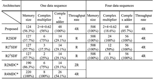
Table II shows comparison of the hardware requirements and throughput rate of various 128-point FFT architectures. For one-data-sequence application, the hardware cost of Module 2, Module 3, and Module 4 in our design is calculated [7]. And the memory size of these modules is only 1/4 of that needed for four-data-sequence application since only one data sequence needs to be stored. The proposed FFT architecture can not only implement three-step radix-8 FFT algorithm in 128-point FFT to reduce the number of complex multiplications but also pro-vide four times throughput rate, compared with SDF scheme, as listed in Table II. In addition, the numbers of memory excluding the input buffer and complex multipliers used in our scheme are only 56.3% and 56% of those in R4MDC architecture.
TABLE II
COMPARISON OF THEHARDWAREREQUIREMENTS ANDTHROUGHPUTRATE OFVARIOUS128-POINTPIPELINEDFFT ARCHITECTURES
Although the number of complex adders in our design is more than that in the others, the cost of complex adder is much less than that of memory and complex multiplier, respectively. The hardware cost of Module 1 Module 2, Module 3, and Module 4 is calculated and listed in Table II. It is clear that the hardware costs of the combinational circuit including complex multi-pliers and complex adders are not increased. But the memory size of our scheme is increased four times because four data sequences will be stored in this approach. In general, the FFT processor dealing with 1–4 simultaneous data sequences uses the multiprocessor approach. Therefore, four FFT processors are needed to calculate four simultaneous data sequences for IEEE 802.11n applications. Since using multiprocessor ap-proach to deal with four data sequences, the hardware costs of R2MDC and R4MDC are very high, thus, the hardware costs of these architectures are not listed in Table II [11]. For this application, our proposed FFT processor provides the required throughput rate with minimal hardware cost, compared with the classical approaches, as listed in Table II.
IV. SIMULATION ANDIMPLEMENTATION
At first, the 128/64-point chosen FFT/IFFT algorithm is coded by MATLAB language. After the chosen FFT/IFFT algorithm is valid, the architecture of the processor was mod-eled in Verilog and functionally verified using Verilog-XL simulator. The word length of our proposed FFT processor is a parameter which can be decided by customers. Based on the simulation results, we determined the word length of the proposed FFT/IFFT to be 12 bits in both real and imaginary parts to meet IEEE 802.11n system requirements. According to the operation clock rate lists in Table I, two clock rates, 40 and 20 MHz, are used for the operation of 128-point and 64-point FFT. And the input sequences are in the specified order when they are loaded into the proposed FFT processor, as shown in Fig. 3. At the operation clock rate of 40 MHz, the computation of 128-point FFT/IFFT with four data sequences requires 3.2 s, i.e., 128 cycles. Furthermore, the computation of 64-point FFT/IFFT with four simultaneously data sequences needs 3.2 s at the operation clock rate of 20 MHz. Due to the execution
TABLE III
AREAPERCENTAGES OF THEBLOCKS IN THEPROPOSEDFFT PROCESSOR
Fig. 11. Layout view of proposed FFT processor.
time of the proposed 128/64-point FFT/IFFT is less than 3.6 or 4 s, our proposed scheme can meet the requirement of IEEE 802.11n.
After functional validation, the proposed architecture is syn-thesized for UMC 0.13- m one-poly eight-metal layer (1P8M) CMOS technology using the Synopsys Design Analyzer. The functional behavior of the synthesized circuit is checked by using Verilog-XL simulator. The area percentages of the blocks in our proposed FFT processor are summarized in Table III. Module 3 occupies the largest area in our design because the modified complex multiplier is used in this module.
After synthesis, automatic place and route is carried out by using Cadence SOC encounter. The core size including the test module is 600 2142 m and the chip area including power ring and input–output (I/O) pads is 1058 2545 m . The func-tion of the test module consisting of 6.144 K-bit SRAM is to save 34 chip pins. Input data are stored serially in the test module from the chip input pins before the operation of the processor. The test module provides 1–4 complex input sequences in par-allel to the FFT/IFFT processor core when the processor begins to work. The 84-pin is used in our chip, where 66 pins are signal pins and others are power pins. The layout view of the proposed FFT processor is shown in Fig. 11. The maximum operation clock rate can be up to 100 M Hz. At the operation clock rate of 40 M Hz, the 128-point FFT with four data sequences can be
LIN AND LEE: DESIGN OF FFT/IFFT PROCESSOR 815
calculated in our proposed FFT/IFFT processor when it meets IEEE 802.11n standard. In this condition, the power consump-tion of the proposed FFT/IFFT processor is only 5.2 mW from primepower simulator.
V. CONCLUSION
A novel 64/128-point FFT/IFFT processor for a MIMO OFDM system has been proposed. In our design, 64-point and 128-point FFT/IFFT can be supported. Based on the concept of data reordering and grouping, the processor can provide different throughput rates to deal with 1–4 simultaneous data sequences more efficiently. Furthermore, the hardware costs of memory and complex multiplier can be saved by adopting delay feedback and data scheduling approaches. And the number of complex multiplications can be reduced effectively by using higher radix FFT algorithm. The proposed FFT/IFFT processor designed in a 0.13- m 1P8M CMOS process can meet IEEE 802.11n standard at the operation clock rate of 40 MHz.
ACKNOWLEDGMENT
The authors would like to thank their colleagues of the SI2 Group, National Chiao Tung University, HsinChu, Taiwan, R.O.C., for fruitful discussion.
REFERENCES
[1] Mujtaba et al., TGn Sync Proposal Tech.Specification for IEEE 802.11 Task Group 2005, IEEE 802.11-04/0889r3.
[2] S. Magar, S. Shen, G. Luikuo, M. Fleming, and R. Aguilar, “An appli-cation specific DSP chip set for 100-MHz data rates,” in Proc. Int. Conf.
Acoustics, Speech, Signal Process., Apr. 1988, vol. 4, pp. 1989–1992.
[3] H. Shousheng and M. Torkelson, “Designing pipeline FFT processor for OFDM (de)modulation,” in Proc. URSI Int. Symp. on Signals, Syst,
Electron., Oct. 1998, vol. 29, pp. 257–262.
[4] J. O’Brien, J. Mather, and B. Holland, “A 200 MIPS single-chip 1 k FFT processor,” in Proc. IEEE Int. Solid-State Circuits Conf., 1989, vol. 36, pp. 166–167,, 327.
[5] B. M. Bass, “A low-power, high-performance, 1024-point FFT pro-cessor,” IEEE J. Solid-State Circuits, vol. 34, no. 3, pp. 380–387, Mar. 1999.
[6] W.-C. Yeh and C.-W. Jen, “High-speed and low-power split-radix FFT,” IEEE Trans. Acoust., Speech, Signal Process., vol. 51, no. 3, pp. 864–874, Mar. 2003.
[7] Y.-W. Lin, H.-Y. Liu, and C.-Y. Lee, “A 1 GS/s FFT/IFFT processor for UWB applications,” IEEE J. Solid-State Circuits, vol. 40, no. 8, pp. 1726–1735, Aug. 2005.
[8] L. Jia, Y. Gao, J. Isoaho, and H. Tenhunen, “A new VLSI-oriented FFT algorithm and implement,” in Proc. 11th Annual IEEE Int. ASIC Conf., Sep. 1998, pp. 337–341.
[9] A. V. Oppenheim and R. W. Schafer, Discrete-Time Signal
Pro-cessing. Englewood Cliffs, NJ: Prentice-Hall, 1999.
[10] E. E. Swartzlander, W. K. W. Young, and S. J. Joseph, “A radix 4 delay commutator for fast fourier transform processor implementa-tion,” IEEE J. Solid-State Circuits, vol. 19, no. 10, pp. 702–709, Oct. 1984.
[11] L. R. Rabiner and B. Gold, Theory and Application of Digital Signal
Processing. Englewood Cliffs, NJ: Prentice-Hall, 1975.
Yu-Wei Lin was born in Tainan, Taiwan, R.O.C.,
in 1975. He received the B.S. degree in electrical engineering from National Sun Yat-Sen University, Kaohsiung, Taiwan, R.O.C., in 1999 and the M.S. and Ph.D. degrees from National Chiao Tung Uni-versity, HsinChu, Taiwan, R.O.C., in 2003 and 2005, respectively.
In 2005, he joined MediaTek Inc., HsinChu, Taiwan, R.O.C., to develop digital TV modem related systems. His research interests include baseband signal processing, VLSI architectures, and SoC designs for communication systems.
Chen-Yi Lee (M’01) received the B.S. degree from
National Chiao Tung University, HsinChu, Taiwan, R.O.C., in 1982, and the M.S. and Ph.D. degrees from Katholieke University Leuven (KUL), Belgium, in 1986 and 1990, respectively, all in electrical engi-neering.
From 1986 to 1990, he was with IMEC/VSDM, working in the area of architecture synthesis for digital signal processing. In February 1991, he joined the faculty of the Electronics Engineering Depart-ment, National Chiao Tung University, where he is currently a Professor. He served as the Director of Chip Implementation Center (CIC) from 2000 to 2003, an organization for IC design promotion in Taiwan. He also served as the Department Chair of Electronics Engineering, National Chiao Tung University (2003– 2006). His research interests mainly include VLSI algorithms and architectures for high-throughput DSP applications. He is also active in various aspects of system-on-chip design technology, very low power designs, multimedia signal processing, and wireless communications.
Dr. Lee was the former IEEE CAS Taipei Chapter Chair (2000–2002), the SIP task leader of National SoC Research Program (2003–2005), and the mi-croelectronics program coordinator of Engineering Division under National Sci-ence Council of Taiwan (2002–2005).
