A 3.1~10.6 GHz CMOS Direct-Conversion Receiver
for UWB Applications
Chung-Yu Wu, Yi-Kai Lo, and Min-Chiao Chen Nanoelectronics and Giga-scale Systems Laboratory, Institute of Electronics, National Chiao Tung University,
Room 307, Engineering Building 4th, 1001 Ta-Hsueh Road, Hsinchu City, Taiwan Abstract—In this paper, a 3.1~10.6 GHz fully integrated
low-power CMOS direct-conversion receiver for ultra-wideband (UWB) applications is proposed and analyzed. The proposed receiver consists of a wideband low-noise amplifier (WLNA), quadrature down-conversion mixers, output I/Q buffers and a carrier generator. This chip was designed in 0.13-um CMOS technology. According to the simulation results, the proposed receiver has noise figure (NF) of 4.1~7.1 dB, receiver voltage gain of 22 dB, and input-referred 1-dB compression point (P1dB) of -22~-26 dBm and third-order intercept point (IIP3) of -12~-16 dBm. It consumes 38.4 mW from 1.2 V power supply.
I. INTRODUCTION
The ultra-wideband (UWB) application is under significant development for high-speed and short-range communication systems. It has great potential in applications of wireless personal-area network (WPAN), such as wireless video distribution systems (WiMedia), wireless USB, and wireless 1394 Firewire[2], [3]. As specified in IEEE P802.15, the radio specification defines an operating spectrum for Multiband-UWB (MB-UWB) from 3.1 to 10.6 GHz and divides it into 5 band groups and 14 bands with spacing of 528MHz as shown in Fig. 1. In the mean time, it provides the robustness in good spectrum efficiency, multipath fading environment, and immunity to narrow-band interference and can coexist with other wireless standards.
Some design problems in the implementation of a UWB transceiver are considered challenging to the designers. For example, a wide frequency range LNA with high linearity, low NF and wideband input matching as well as a wideband local oscillator (LO) generating the needed carriers are required for receiver circuit implementation. These circuit performance requirements should be satisfied under suitable power consumption and minimized cost.
So far, several UWB receivers or transceivers have been reported [4], [5]. In [4], multiple LNAs and PLLs are designed in CMOS technology for the band from 3.1 to 5 GHz. However, it consumes much extra power to achieve little bandwidth increment. In [5], a direct-conversion receiver is designed in BiCMOS technology to 3.1~8.2 GHz UWB applications. The design has high power consumption and low integration capability with CMOS baseband digital circuits.
Figure 1. Frequency plan of MB-OFDM UWB
In this paper, a CMOS RF direct-conversion receiver for the application of Multi-band Orthogonal Frequency Division Multiplexing (MB-OFDM) UWB system has been proposed and simulated in 0.13-um CMOS technology. The proposed receiver can be operated in the whole UWB band (3.1~10.6 GHz) and the wideband input matching issue is solved by the proposed wideband LNA (WLNA) circuit. The desired flat NF performance and linearity are also satisfied with the aid of feedback loop in WLNA. Besides, a novel wideband QVCO is designed to generate required carriers for mixing RF signals to DC. The simulation results show overall NF of 4.1~7.1 dB, receiver voltage gain of 22 dB, P1dB of -22~-26 dBm and IIP3 of -12~-16 dBm. It drains 32 mA from 1.2 V power supply.
The receiver architecture and the RF circuit implementation are described in Section II. Section III presents the simulation results. Finally, the conclusion is in Section IV.
II. RECEIVER ARCHITECTURE AND CIRCUIT
IMPLEMENTATION
One of the popular architectures for receiver front-end is direct-conversion receiver, which provides the advantages of high integrity, low cost, and simple architecture. The DC offset issue encountered in most direct-conversion receivers can be eliminated in UWB applications due to its flexible utility of sub-channels in one UWB band, if the sub-channel near dc carries no information purposely, then it can be filtered out with a dc-notch filter at baseband [3].
The block diagram of the proposed receiver is shown in Fig.2, which consists of a wideband LNA (WLNA), I/Q quadrature down-conversion mixers, output I/Q buffers and a carrier generator. The RF input signal is amplified by the
Figure 2. The proposed direct-conversion receiver architecture for UWB application
WLNA. Two I/Q down-conversion mixer groups follow the WLNA. The down-conversion mixers are classified into two groups: group one handles the lower band (3.1~5.5 GHz) signals and group two deals with the higher band (5.5~10.6 GHz) signals. By mixing with proper LO signals provided by the carrier generator, the frequency is translated to DC. Extra digital control scheme is used to determine which mixer group is on, thus the desired output signal can be generated at the output buffers. This arrangement of down-conversion mixers would help in solving the spur issue which is more critical in UWB systems than in narrowband systems [3]. While in this proposed receiver, the lower frequency (3.1~5.5 GHz) and higher frequency (5.5~10.6 GHz) signals are separated, thus the LO signals at 3.1~5.5 GHz and its harmonics will not fall in the higher band. It avoids overwhelming the signal at baseband after down-conversion. The carrier generator, one of the building blocks in a frequency synthesizer, is designed in this chip to provide quadrature LO signals. Based upon the architecture shown in Fig.2, the CMOS implementation of WLNA, down-conversion mixer, and carrier generator is described in the following subsections.
A. Wideband Low-Noise Amplifier(WLNA)
Designing a LNA for UWB applications is a difficult task: the performance requirements of wide bandwidth characters for gain, input matching, high linearity, and minimized flat NF must be satisfied simultaneously. In this proposed CMOS WLNA, a two-stage amplifier is designed to reach these requirements. The common-gate stage is applied as first stage to ease the wideband input matching issue and gm-boosting technique [7] is first introduced to LNA design of UWB systems to overcome the inherent high NF character of CG-LNAs. The second stage is designed to enhance the overall gain.
Fig.3 is the schematic of the proposed CMOS WLNA. C1 is used as a bypass capacitor for isolating the dc level and CP is the equivalent pad capacitor at input terminal. L1 resonates with gate-source capacitor, Cgs, of M1 to match the input impedance (1/gm) to 50 ohm system. The input RF
Figure 3. The proposed CMOS wideband LNA circuit
signal is simultaneously feed to M1 source and PMOS M2 gate to be amplified, then with one path through M2, an inverting signal is applied back to M1 gate. This produces a positive feedback at M1 drain terminal, therefore the signal at M1 drain and the equivalent transconductance (gm) of M1 are both enlarged. Then the high NF character of conventional CG-LNAs are reduced with the increased equivalent gm of input MOS, M1 [7]. In the feedback loop, L2 is used to resonate with parasitic capacitance seen at PMOS M2 drain, C2 is a bypass capacitor to isolate dc level and RB is a large resistor which creates an open circuit at desired frequency. Then, R1 and L3 can improve bandwidth. Finally, in order to have sufficient gain over the whole frequency range, a common-source with resistive degeneration amplifier, M3, R2, and L4, is used as second stage.
Since there is a feedback loop in the proposed circuit, the stability of the amplifier is needed to be reexamined carefully. Simulation results show that the WLNA is unconditional stable over the entire UWB operation frequency and this is assured again through the proper function of the proposed receiver.
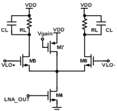
B. Down-conversion Mixer
The circuit schematic of the down-conversion mixer is shown in Fig.4. The CMOS active mixer is based on Gilbert cell core and a single balance mixer structure is selected to eliminate the need of the balun. The WLNA output signal enters driver MOS, M4, the differential LO signals enter the gate of source coupled pair (M5~M6) and an additional gain control mechanism is applied by adjusting the gate voltage of M7. RL and CL are the loading of the mixer.
With the charge injection method [8] in this circuit, the voltage headroom in load resistor (RL) can be relaxed and the bias current of the input transistor can be supplied through it. Since the input transistor, M4, is in saturation region, the conversion gain of the mixer can be increased by increasing the bias current of it. This kind of mixer is duplicated in this receiver circuit, while one receives the lower frequency signals and the other receives higher frequency signals. A special care should be taken in these mixers is that the impedance seen at source node of the source couple pair (M5~M6) varies greatly with widefrequ- ency range. Consequently, the size of M5~M6 should be ad-
justed according to the desired operating frequency for better circuit performance.
C. Carrier Generator
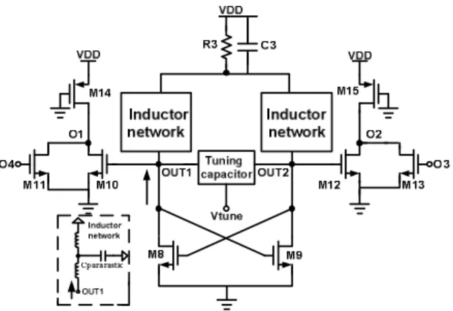
The carrier generator provides the required 3.4~10.3 GHz LO signals in the proposed receiver design and its architecture is shown in Fig.5. The key building block of which is a wideband quadrature voltage-controlled oscillator (QVCO) generating carriers from band #5 to band #14. The QVCO output buffers are used to compensate the difference of the QVCO output power and then follow a divide-by-2 frequency divider at buffer I output to create carriers of band #1 to band #4. Besides, a dummy divider is placed at buffer Q output to minimize the output amplitude and phase mismatch of the carrier generator.
Fig.6 is the proposed CMOS VCO circuit schematic and its inductor network. In the proposed circuit, M8 and M9 forms the cross-coupled pair of the proposed VCO; R3 and C3 are used for biasing the circuit and filtering out high frequency noise to acquire better phase noise performance, respectively. The inductor network is also shown in Fig.6, which is composed of two serious inductors and its parasitic capacitance. This inductor network has a character of decreasing inductance with increasing frequency within the frequency of interests. This can be realized with the advanced 0.13-um copper process due to its high quality factor (Q) and less parasitic [9]. With the aid of these features mentioned above, we can utilize the inductor network before it resonates with its own parasitic and still have a sufficient Q value at the desired frequency. The QVCO circuit is composed of two identical VCO circuits shown in Fig.6. For having a wider tuning range, the output of the proposed VCO, O1~O2, and their inter nodes, OUT1~OUT2 where the extra capacitance seen there seriously degrades the locking frequency range are separated. As a result, what is connected to the QVCO output would have less impact on the locking frequency range. M10~15 are used for quadrature signals generation. Among them, M10 (M12) is used to isolate OUT1 (OUT2) and O1 (O2). M11 (M13) is used to receive output signals of the other duplicated VCO and PMOS M14 (M15) is used as loading. Finally, the QVCO buffers are designed as CS amplifiers and the flip-flop-based frequency divider is adopted to have a wide input frequency range.
III. SIMULATION RESULTS
The UWB direct-conversion receiver is designed and simulated with a.1.2 V supply in 0.13-um CMOS technology. The chip layout is depicted in Fig.7 and total die area is 3.7 mm2. This chip is under fabrication. It can receive the signal from 3.1 to 10.6 GHz at the same time and the required LO signals from frequency band #1 to band #14 are generated by the carrier generator integrated in this receiver. This greatly simplifies the design and future measurement considerations, such as amplitude and phase mismatch causing from off chip circuits and devices. In this CMOS RF direct-conversion receiver, the input is matched to 50 ohm but the output of this receiver does not need to drive 50 ohm impedance. Since
Figure 4. The CMOS down-conversion mixer circuit
Figure 5. The proposed carrier generator architecture
the output signal falls in baseband. For the mixer input port, it is directly connected with WLNA output without any inter stage matching for maximum voltage gain.
Fig.8shows the simulation results of the proposed direct-conversion receiver. The receiver maximum gain is 23 dB at 10 MHz and degrades 2.1 dB at 264 MHz, the simulated minimum cascade NF is 4.1 dB of band #1 input and P1dB is -22~-26 dBm over the entire band in linearity analysis. The input return loss (seen at the WLNA input) remains below -10 dB over the entire operation frequency, as shown in Fig.9.
The gain of this receiver degrades at higher frequency which is on account of unexpected extra parasitic capacitance seen at WLNA output, and consequently, influences the linearity and cascade NF of this receiver. Yet, with the gain control scheme in the mixer circuit, a flat gain performance can be obtained through changing the bias current of the mixer. The currents of the overall receiver, WLNA, I/Q down-conversion mixers and carrier generator are 32 mA, 5.5 mA, 6 mA, and 20.5 mA, respectively. The simulated performance parameters of the proposed direct-conversion receiver are summarized in table I where comparisons with recently published UWB receivers are also listed. Seen that the proposed CMOS UWB direct-conversion receiver has the specified performance with lower power dissipation.
V. CONCLUSION
A 3.1~10.6 GHz CMOS UWB direct-conversion receiver is proposed and analyzed in this paper. The proposed direct-conversion receiver is composed of a WLNA, I/Q quadrature down-conversion mixers and a carrier generator. Designed and simulated in TSMC 013-um 1P8M CMOS process, the
Figure 6. The proposed CMOS VCO circuit and inductor network
proposed receiver has a DSB NF varying from 4.1 to 7.1 dB, voltage gain of about 22 dB, an input P1dB of around -22 dBm, IIP3 of about -14 dBm, and the current consumption is 32 mA from a 1.2 V supply. Future research will be conducted to design and integrate a complete CMOS UWB transceiver for applications in MB-OFDM UWB systems.
ACKNOWLEDGMENT
The authors would like to thank the Chip Implementation Center (CIC) and National Science Council, Taiwan for the fabrication of the testing chip.
REFERENCES
[1] Physical Layer Submission to 802.15 Task Group 3a:Multi-band Orthogonal Frequency Division Multiplexing, IEEE P802.15-03/268r2.
[2] S. Roy, J. R. Foerster, V. S. Somayazulu, and D. G. Leeper,” Ultraw- ideband radio design: The promise of high-speed, short-range wireless connectivity,” Proc. IEEE, vol. 92, no. 2, pp. 295-311, Feb. 2004.
[3] Pengbei Zhang and Mohammed Ismail,” A New RF Front-End and Frequency Synthesizer Architecture for 3.1-10.6 GHz MB-OFDM UWB Receivers,” IEEE. Circuits and System., pp. 1119-1122, Aug. 2005.
[4] B. Razavi,F.-R. Yang, K.-Yu. Li, R.-H. Yan, H.-C. Kang, C.-C. Hsu, and C.-C. Lee,"A UWB CMOS Transceiver," IEEE J.Solid-State
Circuits,vol 40, no.12,pp.2555-2562
[5] A. Ismail and A. Abidi “A 3.1 to 8.2 GHz direct conversion receiver for MB-OFDM UWB communications,” in ISSCC, pp. 208-209, Feb. 2005.
[6] Andrea Bevilacqua, Ali M.,” An Ultrawideband COMS Low-Noise Amplifier for 3.1-10.6-GHz Wireless Receivers,” IEEE Solid-State
Circuits, Journals, vol. 39, no. 12, pp.2259-2262, DEC, 2004.
[7] W. Zhuo, X. Li, S. Shekhar, S. H. Embabi, J. Pineda de Gy vez, D. J. Allstot, and E. Sanchez-Sinencio, “ A Capacitor Cross-Coupled Common-Gate Low-Noise Amplifier,” IEEE Trans. Circuits Syst., vol . 52, no. 12, pp. 875-879.
[8] L. A. MacEachern and T. Manku, “ A charge-injection method for Gilbert cell biasing,” in Proc. IEEE Canadian Conf. Electric
Computer Eng., vol. 1, May 1998, pp. 365-368.
[9] N. Fong, J.-O. Plouchart, N. Zamdmer, D. Liu, L. Wanger, C. Plett, and G. Tarr, “A Low-Voltage Multi-GHz VCO with 58% Tuning Range in SOI CMOS,” in IEEE Custom Intergrated Circuits Conf., pp.423-426,2002.
Figure 7. The layout diagram of the designed CMOS direct-conversion receiver
Figure 8. Simulation results of voltage gain, P1dB and NF
Figure 9. Input return loss (S11)
TABLE I. PERFORMANCE SUMMARY AND COMPARISON
Reference [4] This work Bandwidth 3~5 GHz 3.1~10.6 GHz Receiver gain 69~73 dB 20~23 dB Receiver NF 5.5~8.4 dB 4.1~7.1 dB Receiver P1dB -27.5~-29.5 dBm -9.5~-12.5 dBm -22~-26 dBm
Receiver IIP3 None -12~-16 dBm
S11 <-11dB <-10dB Phase Noise -104~108 dBc/Hz -99~109 dBc/Hz
Power 105 mW 38.4 mW Supply voltage 1.5 V 1.2 V
Technology 0.13um CMOS 0.13um CMOS