A New Method for Extracting the Channel-Length
Reduction and the Gate-Voltage-Dependent Series
Resistance of Counter-Implanted p-MOSFET’s
Chien-Min Wu,
Student Member, IEEE, and Ching-Yuan Wu,
Member, IEEEAbstract— Based on the channel-resistance measurement, a new method for extracting the channel-length reduction(1Ljj) and the gate-voltage-dependent source/drain resistance (RSD)
of counter-implanted p-MOSFET’s is proposed, in which the necessity of the applying substrate bias is demonstrated and an empirical relationship between poly-Si gate length (LM) and
device structure parameters for 1Ljj extraction is provided. This is the first attempt to extract the basic parameters of counter-implanted p-MOSFET’s with the LDD structure. Nu-merical analysis using two-dimensional (2-D) device simulator has been used to verify the proposed extraction method. Furthermore, an improved approach to extract RSD is also presented. Both numerical analysis and experimental results show good accuracy of our proposed method.
I. INTRODUCTION
T
HE accurate determination of the channel-length reduc-tion and the parasitic source/drain resistance in MOSFET’s becomes increasingly important for de-vice miniaturization and optimization. Many methods [1]–[10] have been presented to extract the effective channel length based on the resistance method because of its simplicity. However, the previous investigations were almost dedicated to n-MOSFET’s and had their apparent shortcomings for the LDD structure. Recently, these shortcomings have been carefully studied by two-dimensional (2-D) device numeri-cal analysis and the algorithm for accurately extracting the metallurgical channel length of conventional and LDD n-MOSFET’s has been proposed [11]. The accuracy of the proposed method in [11] has been verified by a novel technique based on the charge-pumping method [12].For existing p-MOSFET’s using the n -poly Si technology, counter implantation is usually applied to the channel region for lowering the threshold-voltage in modern CMOS/VLSI fabrication. Compared with existing n-MOSFET’s, the major differences are that there is no metallurgical p-n junction formed along the channel surface and the conduction carriers are widely spread into the counter-implanted layer. Basically, the conduction current between source and drain diffusion islands of counter-implanted p-MOSFET’s consists of two
Manuscript received November 21, 1996; revised April 3, 1997. The review of this paper was arranged by Editor M. Fukuma. This work was supported by the National Science Council, Taiwan, R.O.C. under Contract NSC-86-2215-E009-034.
The authors are with Advanced Semiconductor Device Research Laboratory and Institute of Electronics, National Chiao-Tung University, Hsinchu 300, Taiwan, R.O.C.
Publisher Item Identifier S 0018-9383(97)08298-1.
components: One is due to gate-voltage induced carriers and the other is due to the buried channel carriers. The current contributed by the gate-controlled carriers can be fundamentally modeled by the conventional equation, however, the equation is not suitable for describing the cur-rent contributed by the buried layer due to the diffecur-rent gate-bias dependence and scattering mobility. As a result, the extraction technique for the channel-length reduction of counter-implanted p-MOSFET’s is different from that of n-MOSFET’s. Besides, we will focus on the extraction technique for the gate-voltage-dependent because it is a by-product of extraction based on the resistance method.
In this paper, a new technique based on the resis-tance method for extracting of counter-implanted p-MOSFET’s with either conventional or LDD structure is proposed, in which the substrate bias is applied for accurate extraction and the threshold-voltage is determined by the iterative method. The proper selection of poly-Si gate length with applying that obtained from the numerical simulation is presented for extraction and an improved method to alleviate the discrepancy between the extracted and the actual one is proposed. In addition, the accuracy of the proposed method has been verified by 2-D device numerical analysis and the proposed method is applied to fabricated p-channel MOSFET devices with either conventional or LDD structure.
II. EXTRACTION METHOD A. Extraction
Fig. 1 shows the schematic cross section of a LDD p-MOSFET with counter implantation, where is the intrinsic channel length and is defined as the distance between source and drain junctions in the channel surface;
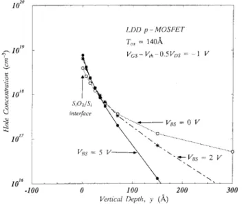
is the channel-length reduction due to lateral diffusion; is the poly-Si gate length. Due to counter-implanted layer, the carrier distribution in p-MOSFET’s is spread wider than that in n-MOSFET’s. Therefore, the conventional model for effective channel length extraction will be challenged, as demonstrated by 2-D device simulation. Fig. 2 shows the simulated hole concentration along the vertical direction under various substrate biases. Evidently, the holes can be squeezed toward the SiO /Si interface with increasing . It can be demonstrated that, as the conduction carriers are
Fig. 1. The cross section view of aLDD p-MOSFET and its definitions.
integrated from the surface to A, the ratio˚ of inversion carrier over can be improved about
21% for V when compared with V.
Since the high ratio corresponds to approaching to surface conduction, the application of is justified in order to use the conventional linear-region equation based on the charge-sheet approximation. Under higher , the total drain-to-source resistance for the extrinsic device operated in the linear region can be expressed as
(1)
where and ;
is the source/drain parasitic resistance;
is the gate-drive voltage. is the effec-tive channel-length reduction and the others have their usual meanings. As discussed before, (1) holds only for surface-conduction devices. Due to the channel broadening effect, the intrinsic channel-resistance of counterimplanted -MOSFET’s becomes smaller. Since the bias-dependent can interfere extraction [4], must keep much higher than . In this paper, the application of higher can ensure counter-implanted p-MOSFET to be operated in surface conduction mode and can increase the value of , and hence (1) is more valid for extraction and higher accuracy is expected at larger .
To demonstrate the effect on channel length extraction, a 2-D device simulator—SUMMOS [13] is used to generate the data. From Fig. 1, the lateral source/drain profile near the source/drain junction is approximated by Gaussian-tail function and the length of is defined to be the distance between the intrinsic channel edge and the beginning diffusion-point of p lateral profile for LDD structure. This definition is still applicable for the conventional structure by replacing the lightly-doped region with the heavily-doped p region. LDD and conventional counter-implanted p-MOSFET’s with various poly-Si gate lengths (0.4 m 10 m), a gate width
of m, A and˚ m
are used as inputs to SUMMOS. It should be noted that accurate determination of the threshold voltage is very important for (1) especially for small-dimension devices. The conventional linear extrapolation method is sensitive to
Fig. 2. The hole concentration as afunction of the vertical depth for different substrate biases andVGS0 Vth0 0:5VDS = 01 V.
Fig. 3. The extracted1L versus VGTat differentVBS’s. The insert shows the variation of local maximum1Lmax with VBS. The peak value in the insert is found to be the extracted1Lext.
and is inappropriate for threshold-voltage determination. Here, is obtained iteratively by the normalized current method [11]. For a given , the family of with various gate drives obtained by the linear regression technique can be used to establish a set of values. According to the closely-separated- method [6], the extracted is gate-bias dependent. Similar extractions can be practiced by changing , as shown in Fig. 3. Because is -and -dependent, the determination of from Fig. 3 is the major concern in this paper.
Fig. 3 illustrates the effects of and on the extracted for counter-implanted p-MOSFET’s. The LDD device shows the stronger -dependence due to the carrier density modulation by the gate field in the lightly doped source/drain region. Because is a parameter to be extracted, the elec-trical channel length must be prevented from modulation. For a given is far away from the exact as
increases due to the extension of effective channel region, and can be approached at low . As approaches zero, a deviation from the monotonically increasing behavior with decreasing projects the invalidity of the linear-region equation near the subthreshold-region operation. This physical feature is the same as those shown in [3], [4], [11]. However, the degree of this deviation is further enhanced for p-MOSFET’s because the drain current is dominated by the conduction in the buried layer. The local maximum of at low as shown in Fig. 3 can be reasonably taken as the temporarily extracted value for each . Since under changing has different , the relationship between and can be obtained, as illustrated in the insert of Fig. 3. It is clearly evident that the conventional method, which confines the channel-length reduction extracted at V, is very inaccurate and the error in extraction is over 40%. As seen in the insert of Fig. 3, due to the spill-over effect of the carriers [10], increases initially with and is gradually approaching the exact (i.e., 0.2 m). As expected, this result is self-consistent with the previous analysis and demonstrates that the applying is indispensable for -MOSFET’s. This distinctive feature is very different from that of -MOSFET’s. The saturation behavior for may be regarded as the necessary condition for accurate extraction. Here, we choose the peak value (see the insert of Fig. 3) as the extracted channel-length reduction
.
In addition to the effect, we also find that the choice of combination can slightly influence the extracted values, as pointed out in [8], [9]. Fig. 4(a) shows the different extracted results. Note that and denote the maximum and minimum poly-Si gate lengths used for extraction, respec-tively. The deviations from the given value are considered to be caused by the small-dimension effect and the fluctuations in linear regression process [9], and the error should be corrected. As shown in Fig. 4(a), the intersecting point for the extracted equal to with each curve determines the gate length (i.e., ) needed for correct extraction.
Careful examination of versus , we find
that the product of is nearly independent of the selected . This makes the combination choice more flexible with only keeping the value of . To complete the numerical analysis, different oxide thickness ( A) and source/drain lateral diffusion profiles˚
( m) are used to construct by
directly comparing with the exact given . The data points shown in Fig. 4(b) are determined under the applying and each point coincides with the given value. It’s interesting that the data points with different stucture parameters locate on their universal curves. An empirical equation is used to fit the data points, which reads
for CONV. devices for LDD devices (2) where and are in m. The lines in Fig. 4(b) are
generated by (2) with m, m and
m , m . It is shown that different source/drain doping gradient can affect the extraction result.
In [3], Sun et al. had proposed that the extraction error in can be minimized whenever the modulated is much less than the change in . Since the gradual junction profile (larger ) has the increasingly gate-modulated , choosing the longer as the reference device is needed to suppress the extraction error. For this reason, the gate voltage can easily modulate the lightly doped source/drain, exhibits much stronger structure-dependences on and for LDD devices. Moreover, compared to conventional device, LDD device has the larger value of and this reflects that longer combination for extraction is essential in order to reduce the interference of . Hence, has the larger value as shown in Fig. 4(b). On the other hand, for the conventional structure with heavy doping, the value mainly depends on the source/drain doping gradient but is hardly influenced by gate field, and hence, plays only
a minor role in extraction. So, becomes
-independent and is related to only. As can be seen
in Fig. 4(b), when m is used,
with A and˚ m can be accurately
determined to be 0.201 m ( m) for LDD devices.
However, for the case of A and˚ ,
the extracted is 0.231 m if m
is still used for extraction, and the extraction error is about 16%, as shown in Fig. 4(a). This suggests that, to extract accurately, must be properly chosen for devices with different technologies, especially for LDD devices. The extracted channel-length reduction according to (2) can be assigned to be .
To further verify the validity of the proposed extraction method, the numerical devices with different channel profile, lateral diffusion ratio of source/drain island, contact resis-tance, or are also examined. The proposed method is implemented to extract the channel-length reduction and the extracted value is directly compared with the given value. The extraction results have demonstrated that the extraction errors in channel-length reduction are within 3% and good accuracy can be obtained. This indicates that the proposed extraction method is valid for the counter-implanted p-MOS device. B. Extraction
In this study, is defined as the parasitic resistance outside and, therefore, the gate-voltage-dependence of can be theoretically obtained by drawing a vertical line at
in the plot and the intercepts with these straight lines give . It means that
can be determined by
(3) Fig. 5 shows comparisons between numerical analysis and extracted . It is clearly seen that the extracted results are underestimated and the deviation is enhanced for low . The insert in Fig. 5 can explain this phenomenon. Obviously, the calculated across the intrinsic channel region is assumed to be constant for the extraction method and its magnitude is nearly equal to the exact numerical value at the middle point of the channel. However, the channel resistance near
(a)
(b)
Fig. 4. (a)1LextversusLmaxfor differentL0mins. L0maxmeans the mask length needed for correct extraction; (b)xp(xp=Tox) versus L0max2 Lmin for conventional (LDD) devices. The data points are extracted from the numerical simulation and the lines are computed from (2).
the source/drain junction in real situation is less modulated. This is partially attributed to the fact that some normal electric fields under the gate are terminated by the source/drain island; the other is that there exists the ambiguous junction between the channel surface and the source/drain island due to the counter-implanted channel. Therefore, the source/drain diffusion tail can extend into the counter-implanted channel and the excess holes near the source/drain junction will be increased. These excess holes behave as if they are a part of the source/drain diffusion region. As a consequence, these two effects overestimate the extracted and lead to the underestimation of the extracted . Fig. 5 also shows that, even for higher , the deviation of between them can be still observed. This can be explained by the carrier spill-over effect near the source/drain. Based on this understanding, we cannot accurately determine both and simultaneously, but an effective length can be defined by integrating the exact numerical curve and dividing by , as
shown in the insert of Fig. 5. Therefore, the length reduction, which satisfies the exact , can be evaluated by
(4)
where is calculated by , and the
increased amount in is
(5) Fig. 6 shows the calculated results for p-MOSFET’s with various device parameters, in which different given ’s are also examined. The average for all ’s
is plotted in the insert of Fig. 6. As pointed out before, the underestimation of is due to the lateral electric field emanating from the source/drain island and the carrier
spill-over effect. However, the change of and
can only affect the normal field. For this reason, is nearly independent of the variations of and . As shown in the insert of Fig. 6, the variation ranges of for the LDD and conventional structures are strictly confined to about 0.031
m and 0.021 m , respectively. It should
be noted that the doping level in the LDD structure (10 cm ) is much less than that in the conventional structure (10 cm ), leading to the reduction of the lateral field and the stronger control capability of the normal gate-field near the channel edge. As a result, the larger can be expected due to the reduced , and hence the correction term of LDD devices has the larger value. Although a steep source/drain junction profile can slightly increase the lateral field, it is the second-order effect. Based on this observation, represents the average length over which the source/drain junctions are blurred and its amount is much dependent on the source/drain doping level. For simplicity, of p-MOSFET’s can be newly extracted as
(6) As discussed previously, looks as if the extension of the source/drain for counter-implanted p-MOSFET’s. Although may depend on different technologies, its physical reason for its nonvanishing value has been clearly stated. Fig. 7 shows comparisons of between numerical analysis and improved extraction method for LDD devices. Note that the universal property can be observed from the numerical data
of for various . For V the devices
are operated in turn-on linear-region, the extracted is very accurate and is consistent with . It also shows that some deviations can be still observed for lower because the drain current is dominated by subthreshold conduction in the buried-layer. In this region, due to the linear-region equation used, the drain current will be overestimated and
will be underestimated, and therefore, it leads to the slightly overestimation of . Nevertheless, the agreements are quite good for wide-range and various device sructure parameters. As compared to counter-implanted p-MOSFET’s, the actual near the source/drain junction is nearly equal to the extracted value at the middle point of the channel for n-MOSFET’s because the lateral field of abrupt p-n junction is
Fig. 5. Comparisons between numerical analysis and extracted RSD at
LM= 1Lext(= 1Ljj) for LDD device. The insert shows comparisons of
dR=dx between numerical analysis and extraction results for various V0 GTs.
Fig. 6. 1L0 versus VGT for conventional and LDD p-MOSFET’s with variousTox; xp, and1Ljj. The insert shows the variations of1 for these devices.
much higher and the carrier spill-over effect doesn’t occur, and hence can be neglected, as shown in [11]. This distinctive feature is different from that of p-MOSFET’s.
III. APPLICATION TOFABRICATED DEVICES
Several sets of experimental counter-implanted p-MOSFET’s are tested here. The first set was fabricated by the 0.5 m n-well CMOS technology with
˚
A for both conventional and LDD structures. The second and third sets used consist of a series of p-channel LDD MOSFET’s fabricated using the 0.7- m technology with
˚
A and the 1.0- m technology with ˚
A, respectively. All devices have the same poly-Si gate
width ( m), and the data are measured at
V by HP4145B. For practical application, we assume that the lateral doping in the p region along
Fig. 7. Comparisons between numerical analysis and extracted RSD at
LM= 1Ljj+ 1 [see (6)] for LDD devices with different device structure parameters.
the surface begins to diffuse at the poly-Si gate edge (i.e., ), and this can be reasonably regarded as the general/central case for the actual devices. We first take a fixed and choose different to extract the corresponding . Similar calculations can be performed by changing and is evaluated by . The extracted results are shown in the insert of Fig. 8 and (2) for LDD devices is also plotted for extraction. It is observed that the intersecting points for various curves with (2) are nearly confined at a common point when is varying from 0.65 m to 0.9 m. This feature clearly demonstrates that our extraction method is very reliable. Then, the channel-length reduction can be determined by
(7) where is -value at the intersecting point times . Similar procedure can be performed for conventional devices. Applying our extraction method and the conventional method to the experimental devices, comprehensive extraction results are listed in Table I. TK57097-2 and TK57097-10 are the conventional devices but have different implanted doses in -well and counter-implanted layer. It is clearly seen that the values of extracted (0.198 and 0.194 m) are very close for our extraction method. This fact supports that, for conventional structures with heavily doped source/drain, the channel-length reduction is less sensitive to the change of implantation dosages because the lateral profile near the source/drain junction has a steep gradient. TK57097-11 and TK57097-15 have the same LDD structure parameters except for adjustment, and implant was added in the channel region with an energy of 50 KeV. The former is implanted with a dose of cm and the latter with a dose of cm . As a result, the spill-over length of carrier concentration for TK57097-15 is longer than that of TK57097-11 due to higher dosage. This behavior looks like the extension of the source/drain region, hence the extracted for TK57097-15 is larger than that of TK57097-11.
TABLE I
THEEXTRACTEDRESULTSFROMEXPERIMENTALDEVICESUSING THECONVENTIONALMETHOD ANDOUREXTRACTIONMETHOD
Fig. 8. Comparisons between experimental data and extracted RSD. The extracted results of the improved method and the original one [see (3)] are also compared. The insert shows the application of (2) to the extraction of the channel-length reduction for experimental devices.
Obviously, a larger wide-range variation of can also be observed. Due to the ambiguous junction for the LDD structures, the channel-length reduction is much influenced by the lateral doping gradient. This implies that careful monitor of the fabrication process is absolutely needed to precisely control its value. More evidence of our extracted has been examined by comparing the DIBL and punchthrough effects of experimental short-channel p-MOSFET devices us-ing a 2-D numerical simulator. Simulation results usus-ing our extraction value show good agreements with the measured subthreshold characteristics (DIBL & punchthrough) for short-channel devices. However, the conventional method always gives the lower value of , leading to the underestimation of the simulated subthreshold .
To demonstrate the validity of the extraction method for , both of conventional (TK57097-2) and LDD (TK55001) devices are tested. In general, is composed of the contact resistance, the sheet resistance, the spreading resistance, and the accumulation layer resistance. For purely experimental
measurements, it is very difficult to obtain the reliable due to the limited resolution of the equipment. Over the past years, the use of a 2-D device simulator has proven to be particularly useful to obtain realistic . In this paper, the simulation output data from SUMMOS are analyzed by a post-processor program, and then the exact can be evaluated through the simulated values of the hole quasi-Fermi potentials in the device structure and the total drain current [8]. Therefore, the basic device parameters are calibrated first by 2-D device simulator. This method employed in determining experimental as a function of is very reliable. Fig. 8 shows experimental data and extracted , and the extracted results of the proposed method and the uncorrected approach are also compared. The values of for TK57097-2 and TK55001 used in the offset method are 0.219 m and 0.179 m, respectively. The reason for the deviation between experimental data and our proposed method at very low has been explained in the previous section. Although this small deviation occurs, good agreements for wide-range can be obtained by the proposed method, while (3) shows poor accuracy. Therefore, the extraction method has its physical meanings.
IV. CONCLUSION
A new method based on channel-resistance measurement to extract both the channel-length reduction ( ) and the gate-voltage-dependent source/drain resistance for counter-implanted p-MOSFET’s has been proposed. The iterative threshold-voltage determination has been implemented into the extraction method. Moreover, we particularly emphasizes on the application of the substrate bias to extract and its validity has been justified. Since conventional and LDD p-MOSFET’s have different source/drain structures, LDD de-vices show the stronger gate-dependence of and . With applying , the empirical equation of
has been established by our numerical simulation and the relationship is reflected from the different degree of gate modulation in the source/drain region. It can provide a guide for the choice of poly-Si gate length combination for extraction and can be well appilcable to our experimental devices. Simulations on the subthreshold using our extracted show good agreements with the measured data. This paper also demonstrates that the extracted will be underestimated if the extracted channel-length reduction is ex-actly equal to , and this can be attributed to the ambiguous junction and the shielding effect of lateral electric field near the source/drain edge. The offset length is introduced to account for these effects. Substituting for , satisfactory agreements can be obtained. Both numerical analysis and experimental results show good accuracy and reliability of the proposed extraction method.
REFERENCES
[1] K. Terada and H. Muta, “A new method to determine effective MOSFET channel length,” Jpn. J. Appl. Phys., vol. 18, p. 953, 1979.
[2] J. G. J. Chern, P. Chang, R. F. Motta, and N. Godinho, “A new method to determine MOSFET channel length,” in IEEE Electron Device Lett., vol. EDL-1, p. 170, 1980.
[3] J. Y. C. Sun, M. R. Wordeman, and S. E. Laux, “On the accuracy of channel length characterization of LDD MOSFET’s,” IEEE Trans.
Electron Devices, vol. ED-33, p. 1556, 1986.
[4] G. J. Hu, C. Chang, and Y. T. Chia, “Gate-voltage-dependent effective channel length and series resistance of LDD MOSFET’s,” IEEE Trans.
Electron Devices, vol. ED-34, p. 2469, 1987.
[5] D. J. Mountain, “Application of electrical effective channel length and external resistance measurement techniques to a submicrometer CMOS process,” IEEE Trans. Electron Devices, vol. ED-36, p. 2499, 1989. [6] J. Ida, S. Ishii, and F. Ichikawa, “Accurate characterization of gate-n0
overlapped LDD with the newLe extraction method,” in IEDM Tech.
Dig., 1990, p. 219.
[7] K. K. Ng and J. R. Brews, “Measuring the effective channel length of MOSFET’s,” IEEE Circuits and Devices Mag., vol. 6, p. 33, 1990. [8] S. E. Laux, “Accuracy of effective channel length/external resistance
extraction algorithm for MOSFET’s,” IEEE Trans. Electron Devices, vol. ED-31, p. 1245, 1984.
[9] K. Terada, “Suppression of measurement errors in effective-MOSFET-channel-length extraction,” in Proc. IEEE Int. Conf. Microelectronic Test
Structures, 1992, p. 208.
[10] S. Hong and K. Lee, “Extraction of metallurgical effective channel length in LDD MOSFET’s,” IEEE Trans. Electron Devices, vol. 42, p. 1461, 1995.
[11] Y. S. Jean and C. Y. Wu, “A new extraction algorithm for the metallurgical channel length of conventional and LDD MOSFET’s,”
IEEE Trans. Electron Devices, vol. ED-43, p. 946, 1996.
[12] H. H. Li and C. Y. Wu, “A novel extraction technique for the effective channel length of MOSFET devices,” IEEE Trans. Electron Devices, vol. ED-42, p. 856, 1995.
[13] R. K. Perng, P. S. Lin, and C. Y. Wu, “A new methodology for developing a fast two-dimensional MOSFET device simulator,”
Solid-State Electron., vol. 34, p. 635, 1991.
Chien-Min Wu (S’92) was born in Tainan,
Tai-wan, R.O.C., on July 14, 1967. He received the B.S. degree in electrical engineering from National Central University, Taiwan, in 1990. Since 1991, he has been pursuing the Ph.D. degree at the In-stitute of Electronics, National Chiao-Tung Univer-sity, Hsinchu, Taiwan. His current research interests focus on characterization and modeling for counter-implanted p-MOSFET’s.
Ching-Yuan Wu (M’72) was born in Taiwan,
R.O.C., on March 18, 1946. He received the B.S. degree from the Department of Electrical Engineering, National Taiwan University, Taipei, in 1968, and the M.S. and Ph.D. degrees from the State University of New York (SUNY) at Stony Brook, in 1970 and 1972, respectively.
During the 1972–1973 academic year, he was appointed as a Lecturer at the Department of Electrical Sciences, SUNY, Stony Brook. During the 1973–1975 academic year, he was a Visiting Associate Professor at National Chiao-Tung University (NCTU), Hsinchu, Taiwan. In 1976, he became a Full Professor in the Department of Electronics and the Institute of Electronics, NCTU. At NCTU, he was the Director of Engineering Laboratories and Semiconductor Research Center from 1974 to 1980; the Director of the Institute of Electronics from 1978 to 1984; and the Dean, College of Engineering, from 1984 to 1990. He was a principal investigator of the National Electronics Mass Plan-Semiconductor Devices and Integrated-Circuit Technologies from 1976 to 1979, and a Coordinator of the National Microelectronics Researches and High-Level Man-Power Education Committee, National Science Council, R.O.C., from 1982 to 1988. He has been the Research Consultant of the Electronics Research and Service Organization (ERSO), ITRI; a member of the Academic Review Committee, the Ministry of Education; and the Chairman of the Technical Review Committee on Information and Microelectronics Technologies, the Ministry of Economic Affairs. His research activities have been in semiconductor device physics and modelings, Integrated-circuit designs and Technologies. His present research areas focus on the developments of efficient 2-D and 3-D simulators for deep-submicrometer semiconductor devices, design rules and optimization techniques for deep-submicrometer CMOS devices, and key technologies for deep-submicrometer CMOS devices. He has published over 180 papers in the semiconductor field and has served as a reviewer for international journals such as IEEE ELECTRON DEVICE LETTERS, IEEE TRANSACTIONS ONELECTRONDEVICES, and Solid-State Electronics.
Dr. Wu is a member of the Honorary Editorial Advisory Board of Solid-State Electronics. He received the Academic Research Award in Engineering from the Ministry of Education (MOE), in 1979 and the outstanding Scholar Award from the Chinese Educational and Curtural Foundation in 1985. He has received the Outstanding Research Professor Fellowship from the Ministry of Education and the National Science Council (NSC), R.O.C. He received the Distinguished Engineering Professor Medal Award from the Chinese Engineering Society in 1992.
![Fig. 8. Comparisons between experimental data and extracted R SD . The extracted results of the improved method and the original one [see (3)] are also compared](https://thumb-ap.123doks.com/thumbv2/9libinfo/7690458.143275/6.918.95.412.156.472/comparisons-experimental-extracted-extracted-results-improved-original-compared.webp)
