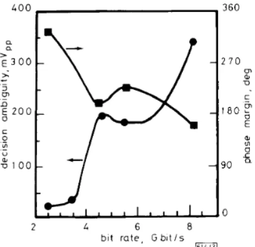
decision threshold ambiguity width (DTAW) and the phase margin (PM). The DTAW is defined as the minimum data input required to obtain an error rate of less than 1 x
The PM is the maximum extent of the phase difference between the clock and the data under 0.8 V peak-to-peak data input and under the above mentioned error rate.3 The mea- sured DTAW and PM against data rate are plotted in Fig. 3.
L O O Q a > E 300 >; c” n
-
25
2 0 0% l o o
C 0 L” U 360-
2 7 0 m aJ U G E-
1 8 0 al m 0 c - 9 0 a 1 , I 1 I , I I 1 1 ,O 2 r, 6 8 bit rate, G b i t / s 161413/Fig. 3 Decision threshold ambiguity width and phase margin for deci- sion circuit against data rate
Demultiplexing can be achieved with the use of master- slave D-type flip-flops in a series-to-parallel convertor or in a parallel processing arrangement, where two flip-flops demulti- plex alternating bits from the input sequence. Demultiplexing operation using the latter architecture was verified by demulti- plexing a single channel up to 11.2Gbit/s. This was accom- plished by using data and half the clock frequency as inputs to the IC. A bit error rate of less than 1 x was measured, along with a phase margin (phase shift of the j72 clock relative to the 11.2 Gbit/s data) of 50.5 deg. The 11.2 Gbit/s input eye pattern and the resulting demultiplexed eye are shown in Figs. 4a and b, respectively.
its relatively mature process and proven reliability as well as its low-cost potential, could play an important role in high- speed lightwave communication systems of up to 10Gbit/s, or even higher data rates.
We would like to thank J. Gannett for the connectivity checks, and D. Daniel and R. D. Standley for stimulating discussions. 1st August 1989 K. RUNGE J. L. GIMLETT D. CLAWIN? W. WAY N. K. CHEUNG Bellcore
331 Newman Springs Road, Red Bank, N J 07701, U S A
I. KIPNIS C. SNAPP Auantek Inc.
39201 Cherry Street, Newark C A 94560, U S A
t
Present address: Fraunhofer Institute-IMS, Finkenstrasse 61, D-4100 Duisberg 1, Federal Republic of GermanyReferences
GIMLETT, J. L., IQBAL, M. Z., ZAH, C. E., YOUNG, J., CURTIS, L., SPICER, R., CANEAU, C., FAVIRE, F., MENOCAL, S. G . , ANDREADAKIS, N., LEE, T. P., CHEUNG, N. K., and TSUJI, s.: ‘A 94 km, 11 Gb/s NRZ transmis-
sion experiment using a 1540nm DFB laser with an optical ampli- fier and a PIN/HEMT receiver’. OFC ’89 Postdeadline Papers, PD16, Feb. 1989
BAGHERI, M.: ‘1 1.4 Gb/s multiplexer for future broadband commu-
nication networks’. Proceedings of the IEEE Bipolar Circuits and Technology Meeting, 1989
SUZUKI, M., HAGIMOTO, K., ICHINO, H., and KONAKA, s.: ‘A bipolar monolithic multigigabit/s decision circuit’, IEEE J. Solid-state Circuits, 1984, SC-19, (4)
REIN, H. M., and REIMANN, R. : ‘3.8 Gbit/s bipolar master/slave D-flip-flop IC as basic element for high-speed optical communica-
tion systems’, Electron. Lett., 1986, 22, pp. 543-544
OHHATA, M., HAGIMOTO, K., and KATO, N . : ‘Above 8-Gb/s GaAs monolithic flip-flop IC‘s for very high-speed optical transmission systems’. GaAs Symposium, 1988
LEUNG, c. c . , LO, T., D U R A , M., KIPNIS, I., KUKIELLA, 1. F., and SNAPP, c.: ‘Bipolar process produces Si MMIC building blocks’, Microw. RF, 1988,27, ( 5 )
0 100 200 300 400 500 time. p s
a
THROUGHPUT EFFICIENCY OF STRATEGIES UNDER MARKOV MODELS SOME ARQ ERROR 1 , l , I r I 1 0 100 200 300 LOO 500 time,ps b F14/LI Fig. 4
a 11.2Gbit/s NRZ test signal at demultiplexer input
b 5.6 Gbit/s demultiplexed eye
Conclusion : In conclusion, we have designed and implemented a submicron silicon bipolar D-type flip-flop integrated circuit which can be employed either as a decision circuit or a demul- tiplexer, operating at data rates substantially higher than pre- viously reported silicon bipolar flip-flop integrated circuits, and with performance comparable to or better than, state-of- the-art GaAs IC technology. The performance of our inte- grated circuit indicates that silicon bipolar technology, with
ELECTRONICS LEVERS 28th September 1989 Vol. 25
Indexing terms: Telecommunications, Errors
Data transmission.
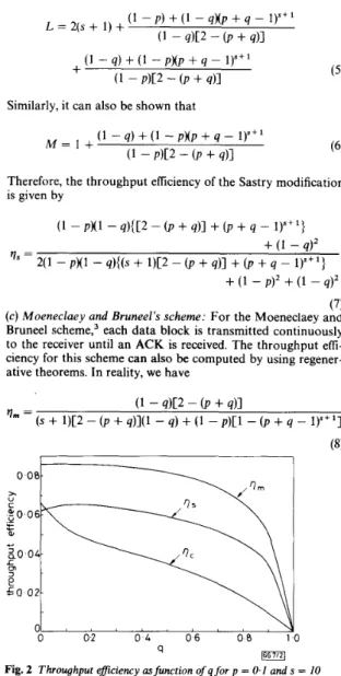
In the letter we compute and compare the throughput efi- ciencies of three continuous ARQ strategies under Markov error models. The three strategies are the classic geback-N, the Sastry modification, and the Moeneclaey and Bruneel scheme. Results show that Sastry’s modification is out- performed by either the classic geback-N scheme or the Moeneclaey and Bruneel scheme.
Introduction: Automatic repeat request (ARQ) strategies are common techniques used to handle transmission errors. S t o p and-wait, go-back-N, and selective-repeat are the three most popular ARQ strategies in use and have been extensively studied. The independent error assumption is often adopted to simplify the analysis of ARQ strategies. This assumption, however, is not realistic for channels where transmission errors occur in bursts. Markov error models are usually used to describe the behaviour of such channels.
In this letter we compute and compare the throughput effi- ciencies of three ARQ strategies under Markov error models. The three ARQ strategies are classic geback-N, Sastry's modification,' and the one proposed by Moeneclaey and B r ~ n e e l . ~ By a Markov error model is meant that the prob- ability that a particular data block arrives at the receiver with error depends on whether the immediately preceding trans- mission is a success or a failure. Generally, a Markov channel can be described as follows. Let X i denote the outcome of the transmission in the ith slot so that X i = 0 means the transmis- sion is a success and
X i
= 1 means the transmission is a failure. Then the error model can be described by P [ X i + =O I X i =
01
= p and P I X i + l = 1 J X i = 13 = q. For conve- nience. letdenote the state transition matrix. It is clear that p
+
q = 1 corresponds to the independent error model. Moreover, it can be shown4 that the k-step transition matrix is given by2 - ( P + q ) 1 - q 1 - p Tk =
( P + q - l ) k 1 - p p - 1
+
2 - ( P + q )[
q - 1 1 - qI
For convenience, we use t f j (i, j = 0, 1) to denote the (i, j)th entry of Tk.
Throughput @ciency: The throughput efficiency of an ARQ scheme is defined as the inverse of the expected number of transmissions to deliver successfully a data block. For simpli- city, we assume that round-trip delay s is fixed and is equal to an integral number of blocks. Notice that round-trip delay is defined as the interval between the end of a transmission and the receipt of its response. In the following, we consider separately the three ARQ strategies of interest under the assumption of a noiseless feedback channel:
__
c y c l e 1-
-
cycle 2-
start of
transm,srmJOOO1 1 010 1110 110 0001 1 011 1111110 001 000000~ 1 . .
s z 3 s = 3 s z 3 s = 3
a
Fig. 1 Typical transmission sequence of Sastry scheme for s = 3 ( a ) Classic go-back-N ARQ scheme: Since the classic go- b a c k 4 ARQ strategy is well known its operation is not explained here. The throughput efficiency of this scheme under Markov error models has been derived' and is given by
(1
-
q)[1 - (P+
q - l)"+'1
(s
+ 1)C2 -
(P+
d I ( 1 - P )+
(1 - q)C1 - (P+
4 - 1)"+l1 (3) 9, =(b) S a s t r y 's modification: The operation of Sastry's modification' is similar to the classic go-back-N ARQ scheme. However, whenever a repeat request is received, the same data block is retransmitted continuously until a positive acknowledgment (ACK) is received. It is noted that the trans- mission sequence of this scheme can be divided into cycles so that each cycle starts with a 1, i.e. an unsuccessful transmis- sion. Fig. 1 shows a typical transmission sequence. By regener- ative theorems," one can compute the throughput efficiency of this scheme by finding the ratio of the expected number of successfully delivered data blocks to the expected number of transmissions in a cycle. Let L and M denote, respectively, the expected cycle length and the expected number of data blocks successfully delivered in a cycle. Then it can be shown that
1348
1
L = 2(s + 1)
+
- [(l-
p)t;o+
&,I
1 - q
After some manipulations, we obtain
( 1 - p )
+
(1 - qxp+
q - I)s+' ( 1 - q ) P - (P+
411
L = 2(s + 1) + ( 1 - 4 )+
(1 - p x p+
q - 1 y + ' (1 - Plc2-
(P+
411+
Similarly, it can also be shown that
( 1 - q ) + ( 1 - p ) ( p + q - 1)"" (1 - Plc2 -
(P
+ 411
M = l + (6)
Therefore, the throughput efficiency of the Sastry modification is given by (1 -
P X ~
- q){C2 - (P+
411+
(P+
4 - I)"+')+
(1 - 4)' 2(1 - PX1 - d { ( s+
1)C2 - (P+ 41 +
(P+
4 - 1)"+') 9 s =+
(1 - P)*+
(1 - 4)' (7)( c ) M o e n e c l a e y and Bruneel's scheme: For the Moeneclaey and Bruneel ~ c h e m e , ~ each data block is transmitted continuously to the receiver until an ACK is received. The throughput effi- ciency for this scheme can also be computed by using regener- ative theorems. In reality, we have
:p
02---
x . L P & a 0 2 - 0 02 0 4 0 6 0 0 1 0 qFig. 2 Throughput efficiency as function of q for p = 0.1 and s = 10
Discussion: When p
+
q = 1, we have qc = (1 - q)/(sq+ l),
in accordance with the results obtained previously under the independent error model. It was shown3 that Sastry's modifi- cation is always outperformed by either the classic go-back-N scheme or the Moeneclaey and Bruneel scheme under the independent error model. The same phenomenon under Markov error models can be observed in Figs. 2-4. Therefore, it seems also unrealistic to use Sastry's modification for Markov channels. Besides, the Moeneclaey and Bruneel
'I.
= (1 - q)/C2sq!l-
4 )+
119 and 9, = (1 - q)/Cs(l - 4)+ 11,
" ' - 1 I
(4) q 1667131
Fig. 3 Throughput efficiency as function of q for p = 0.5 and s = 10
scheme is suitable for noisy channels (i.e. small p and large q), especially when round-trip delay is large.
C I
go
2 1cn
\\
I
01 , 8 j * s ,, U I
0 0 2 0 4 06 0 8 10 1667141 qFig. 4 Throughput efliciency as function of q for p = 0.9 and s = IO
For a Markov channel with state transition matrix
T,
the equivalent block error probability’ is equal to (1 - p ) /(2 - p - q) for the corresponding independent error model. It was proved’ that the classic geback-N ARQ strategy is more efficient for a Markov system than the corresponding system
under the independent error model if and only if p
+
q 2 1. One can easily verify that the conclusion is opposite for the Moeneclaey and Bruneel scheme, i.e. the Moeneclaey and Bruneel scheme is more efficient for a Markov system than the corresponding system under the independent error model if and only if p+
q I 1 .T.-H. LEE 7th August 1989
Department of Communication Engineering National Chiao Tung University Hsinchu, Taiwan, Republic of China
References
1 LEUNG, C. Y., KIKuMOTO, and WRENSON, s. A.: ‘The throughput efliciency of the geback-N ARQ scheme under Markov and related error structures’, IEEE Trans. Commun., 1988, COM-36, 2 SASTRY, A. R . K. ‘Improving automatic repeat-request (ARQ) per- formance on satellite channels under high error rate conditions’, IEEE Trans. Commun., 1975, COM-23, (4), pp. 43-39
3 MOENECLAEY, M., and BRUNEEL, H.: ‘Efficient ARQ scheme for high error rate channels’, Electron. Lett., 1984, 20, pp. 9 8 6 9 8 7 4 cox, D. R., and MILLER, H. D.: ‘The theory of stochastic processes’
(Chapman and Hall, 1965) (2), pp. 231-234
OPTIMISED MULTIPLE QUANTUM WELL PHASE MODULATOR
Indexing terms: Optoelectronics, Optical modulation, Phase modulation, Integrated optics
The quantum confined Stark effect (QCSE) in GaAs/AlGaAs multiple quantum well structures has been shown by several authors to cause large changes of refractive index’.’ and absorption ~ oef lic ie n t~ . ~ near the band edge which are poten- tially of use for phase modulation applications. Hence in a phase modulator there is necessarily a trade-off between the magnitude of the phase modulation, highest near the exciton features, and that of the amplitude modulation. In this letter we report a pin phase modulator that has been optimised for maximum phase change relative to the contrast (ratio of transmission in the ‘on’ state to that in the ‘off state), within certain constraints: the maximum tolerable contrast and the maximum zero bias absorption loss were chosen to be 2 and 50%, respectively. The parameters optimised were the oper- ating wavelength, the number of quantum wells in the active layer and the position of that layer, the operating bias, the device length and the background doping in the intrinsic region. The optimised device was measured to have a phase modulation figure of merit of 27”/Vmm at the optimum bias of 6 V, giving a phase change in a 385 pm-long device of 63 at this bias. The corresponding contrast was approximately 1.4. Photocurrent measurements show that the zero bias absorp- tion loss is also within the 50% limit.
The optimisation process uses data from a single quantum well, normal incidence photodiode to obtain the electric field dependence of an isolated quantum well so as to be able to model the behaviour of waveguide devices.’ Photocurrent data from a normal-incidence pin photodiode incorporating a single 84A GaAs quantum well in the Al,.,Ga,.,As intrinsic region was used to obtain the zero bias absorption coefficient, the change in the absorption coefficient and, via the Kramers- Kronig relation, the change in refractive index for various biases over the wavelength range 820-880nm.6 From the spectra obtained the operating wavelength was optimised for maximum phase change relative to contrast in the absence of waveguiding, bearing in mind that the final device had to exhibit a contrast of less than 2 and a zero bias of less than 50%. The optimum wavelength was found to be 863 nm, some 17 nm below that of the heavy hole excition feature. This set of data was then used to optimise a waveguide device with a 1 pm-thick core of the same refractive index as 84A/60A GaAs/Al,.,Ga,.,As multiple quantum well material. The core could be of this material, of the alloy Al,.,,Ga,.,,As, which has the same index, or some combination of the two. The cladding index was then chosen so that the device would be
ELECTRONICS LETTERS 28th September 1989 Vol.
25
single-mode, and so the cladding material was of A1,.,,GaO.,,As. The modelling was done for T E propagation, since only in this case are the selection rules the same as in the transverse case.’ The details of the model are described in Reference 6. Various device parameters were then varied to optimise for maximum ratio of phase change to contrast within the defined operating constraints.
The optimised structure is shown in Fig. 1. The position and thickness of the quantum well layer, as well as being chosen to reduce amplitude modulation, are chosen so that the device is tolerant of deviations of the background doping, since although the optimum doping was found to be about 5 x 10’6cm-3 it is difficult in practice to control this value sufficiently accurately. The GaAs capping layer is present to facilitate the formation of good ohmic contacts. The structure was grown by atmospheric pressure MOVPE and the con- tacts were evaporated onto the p-type capping layer (Cr/Au) and the n-type substrate (Sn/Au). The contacts were alloyed at a temperature of 440°C for 2min, and then the contacted material was fabricated into slab waveguides approximately 300,um in length. 6 5 x l d 7 c m3 4 x10 c m 0 52 prn A1012Gao88 As I x S h e G a A s 8 x 6 0 A AI0 3Gao 7 A s 4 x 10¹⁵ c m 3 0 3 8 p r n A l o l ~ G a o 8 ~ A s I 4 x l O ” ~ r n - ~ 15 -3
1
prn-
A1015Ga085As[
1
“ I
1
&As substrateFig. 1 Structure of optimised phase modulator
Light from a Coherent 599-01 dye laser using Styryl 9M dye, pumped by a Coherent Innova 1-90 argon ion laser, was end-fire coupled into the devices, and contrast as a function of DC bias was measured using conventional lock-in techniques. The results for a 385 pm long device are shown in Fig. 2, along with the contrast predicted from the model. The phase change as a function of bias in the same device was measured by placing the sample in one arm of a Mach-Zehnder interferom- eter and observing the shift of the fringe pattern. The shifted and unshifted fringe patterns, imaged on a TV camera, were stored in a frame store and each was averaged. By taking the complex Fourier transform of the shifted and unshifted pat- terns one can determine the phase shift from the rotation in the complex plane of the vector corresponding to the spatial