Transient effects of positive oxide charge on stress-induced leakage current in tunnel
oxides
Nian-Kai Zous, Tahui Wang, Chih-Chich Yeh, C. W. Tsai, and Chimoon Huang
Citation: Applied Physics Letters 75, 734 (1999); doi: 10.1063/1.124497
View online: http://dx.doi.org/10.1063/1.124497
View Table of Contents: http://scitation.aip.org/content/aip/journal/apl/75/5?ver=pdfcov
Published by the AIP Publishing
Articles you may be interested in
Stress-induced leakage current and random telegraph signal
J. Vac. Sci. Technol. B 27, 435 (2009); 10.1116/1.3054269
Two-trap model for low voltage stress-induced leakage current in ultrathin SiON dielectrics
J. Appl. Phys. 104, 053718 (2008); 10.1063/1.2969791
Effect of magnetic field on random telegraph noise in the source current of p-channel metal–oxide–semiconductor field-effect transistors
Appl. Phys. Lett. 83, 710 (2003); 10.1063/1.1596381
Improved model for the stress-induced leakage current in thin silicon dioxide based on conduction-band electron and valence-band electron tunneling
J. Appl. Phys. 91, 1577 (2002); 10.1063/1.1429799
Analysis of the stress-induced leakage current and related trap distribution
Appl. Phys. Lett. 75, 3871 (1999); 10.1063/1.125484
This article is copyrighted as indicated in the article. Reuse of AIP content is subject to the terms at: http://scitation.aip.org/termsconditions. Downloaded to IP: 140.113.38.11 On: Thu, 01 May 2014 08:21:24
Transient effects of positive oxide charge on stress-induced leakage
current in tunnel oxides
Nian-Kai Zous, Tahui Wang,a)Chih-Chich Yeh, and C. W. Tsai
Department of Electronics Engineering, National Chiao-Tung University, Hsin-Chu, Taiwan, Republic of China
Chimoon Huang
Winbond Electronics, Hsin-Chu, Taiwan, Republic of China
共Received 18 December 1998; accepted for publication 3 May 1999兲
The role of positive oxide charge in excess low-level leakage current in tunnel oxides induced by Fowler/Nordheim stress is investigated. A correlation between stress-induced gate current and substrate current in an n-channel metal-oxide-semiconductor field-effect transistor is observed. Both the gate current and the substrate current exhibit a significant transient effect. The mechanisms of the stress-induced currents and their field dependence are explored. Positive oxide charge tunnel detrapping is found to be the cause of the observed transient behavior in the two currents. The stress-created positive oxide charge can be significantly annealed by substrate hot electron injection. © 1999 American Institute of Physics.关S0003-6951共99兲02226-3兴
High field stressing during program/erase cycles in flash electrical erasable programmable read-only memory 共EE-PROM兲 operation can lead to an increase in pretunneling leakage current in a tunnel oxide. Stress induced leakage current共SILC兲 has received much attention recently because of its important significance to the data retention and endur-ance characteristics of a flash memory cell. Although exten-sive research has been performed on SILC, its physical mechanisms still remain controversial. Dumin1 and Ricco2 have shown that neutral trap assisted tunneling is the original cause of SILC. DiMaria and Carter3concluded that positive oxide charge plays no part in the SILC conduction mecha-nism in oxides by Fowler/Nordheim 共FN兲 stress. On the other side, Teramoto et al.4claimed that the excess leakage current induced by FN stress is due to the injected holes produced by high energy electrons. Matsukawa et al.5 have further shown that the positive oxide charge induced leakage current6can be reduced by hot electron injection or ultravio-let共UV兲 irradiation. More recently, results by Meinertzhagen et al.7 have shown that the role of positive oxide charge in SILC changes with stress and measurement polarities. In negative gate bias FN stress, positive charge is created near the Si/SiO2surface
8
and thus plays a more important role in SILC measured at a positive field.
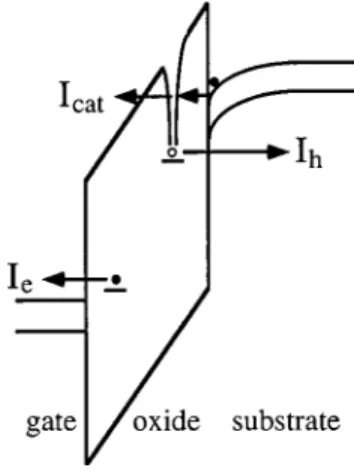
In addition, Dumin and Maddux9found that SILC by FN injection contains a transient component and a dc compo-nent. In their work, the transient current is attributed to nega-tive oxide charge trapping/detrapping and can be character-ized by a 1/t time dependence. Moreover, we have shown that positive oxide charge assisted tunneling current also ex-hibits a transient effect.10The transient behavior arises from the positive oxide charges, which help electrons to tunnel through the oxide, and can themselves escape to the Si sub-strate in measurement. As a result, the SILC transient should consist of three components in general, Ie, Ih, and Icat as
illustrated in Fig. 1, if both positive and negative oxide charges are created during stress. Ie represents negative
ox-ide charge detrapping induced current, Ih is positive oxide charge detrapping current, and Icat denotes positive oxide charge assisted electron tunneling current. Ie and Ih have a t⫺1 time dependence from the tunneling front model9while Icat has a t⫺n time dependence in a certain range of the measurement field. The power factor n is dependent on ef-fective electron and hole tunneling barrier heights and tun-neling masses.10 It should be mentioned that Ih is a hole
current flowing to the substrate and Ieand Icatare an electron
current flowing to the source or the drain. Hence, Ih can be
monitored separately at the substrate while the difference of the gate current (Ig) and the substrate current (Ib) accounts
for the sum of Ieand Icat.
In order to measure the stress induced Ig and Ib at a
small gate bias directly, a large gate area n-channel metal-oxide semiconductor field-effect transistor 共n-MOSFET兲 is specially fabricated. The gate area is 8⫻10⫺3 cm2and the tunnel oxide thickness is about 100 Å. Both positive gate
a兲Electronic mail: [email protected]
FIG. 1. Illustration of three SILC transient components, Ie, Ih, and Icatat a
positive measurement gate bias. The full circles and the open circle repre-sent electrons and holes, respectively.
APPLIED PHYSICS LETTERS VOLUME 75, NUMBER 5 2 AUGUST 1999
734
0003-6951/99/75(5)/734/3/$15.00 © 1999 American Institute of Physics
This article is copyrighted as indicated in the article. Reuse of AIP content is subject to the terms at: http://scitation.aip.org/termsconditions. Downloaded to IP: 140.113.38.11 On: Thu, 01 May 2014 08:21:24
bias FN 共⫹FN兲 stress and negative gate bias FN 共⫺FN兲 stress are performed. The positive trapped charge effects on SILC in the two stressed devices are compared.
Figure 2 shows the transient characteristics of Ig and Ib
by⫹FN stress and ⫺FN stress. The ⫹FN stress is performed at Vgs⫽9.5 V for 400 s and the ⫺FN stress is at Vgs
⫽⫺9.5 V for 400 s. The measurement gate bias is ⫹4 V. In
the figure, the⫺FN stress apparently has a larger SILC. This result is also seen by other researchers11 and the reason will be given. Another feature to be noted in Fig. 2 is the exis-tence of a significant substrate current in the ⫺FN stressed device. In⫺FN stress, electrons emitted from the gate gain kinetic energy in SiO2 and produce electron-hole pairs by band gap impact ionization in the Si substrate. Then, the generated holes are injected into the gate oxide. The appear-ance of the substrate current arises from the discharging of the stress created hole traps and provides direct evidence that positive oxide charge detrapping constitutes an important part in the⫺FN SILC. Conversely, we performed the same measurement in the⫹FN stressed device and Ibis about two orders of magnitude smaller. This distinguished difference suggests that the FN stress created positive charges have a very asymmetrical distribution in the oxide and are accumu-lated near the anode.8 The larger SILC with opposite stress and measurement polarities therefore can be explained by the positive charge detrapping current and the associated posi-tive charge assisted electron tunneling current.
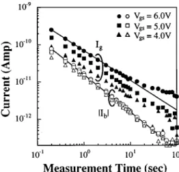
Furthermore, we plot Ig and Ib in the⫺FN stressed de-vice at various measurement voltages in Fig. 3. After each I-t scanning, the ⫺FN stress is applied for 20 s to refill the generated oxide traps. The measurement in Fig. 3 is repeated two times and no significant difference is noticed. The mea-sured SILC and Ib follow a power law time dependence, i.e.,
a straight line on a log-log scale in Fig. 3. However, a close look at the time dependence of the SILC and Ib reveals that
they have a slightly different power factor, especially at a relatively large gate bias. The solid lines in the figure repre-sent a linear fit to the measured results at Vgs⫽6 V. The extracted slope is about⫺0.75 for Igand is ⫺1 for Ib. The
t⫺0.75time dependence of Ig reflects the component of Icat.
The slight deviation of Ig from the straight line at Vgs⫽6 V
for measurement time longer than 20 s is due to a dc
com-ponent in the SILC. In addition, Fig. 3 shows that Ig has a
stronger dependence on the measurement gate bias than Ib
does. As mentioned previously, Ib is caused by positive
ox-ide charge detrapping. The weak field dependence of positive oxide charge detrapping is realized due to a trapezoidal bar-rier for hole tunneling and a large tunneling barbar-rier height. On the other side, Ig is contributed, to a larger extent, by the
electron tunneling currents Ieand Icat. Perhaps because of a
smaller effective electron tunneling barrier or a smaller elec-tron tunneling mass, the elecelec-tron tunneling current exhibits a stronger field dependence. Moreover, the distortion of the local oxide field by a positive trapped charge also makes the electron tunneling barrier somewhat look like a triangular barrier 共Fig. 1兲 and thus increases the field dependence of Icat.
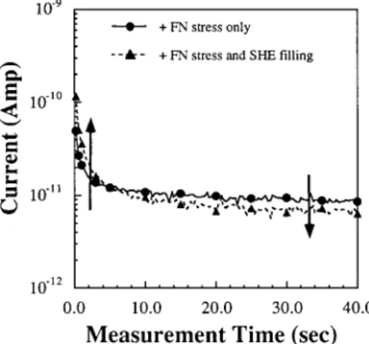
The stress created positive oxide charge can be annealed by using a substrate hot electron 共SHE兲 injection technique. The SHE injection is applied at Vgs⫽2.5 V and Vb⫽⫺7 V for 20 s. Since the injection current is large, the positive trapped charges are neutralized via injected electron and trapped hole recombination. The effects of positive charge neutralization on⫺FN SILC and Ib are shown in Fig. 4. The
FIG. 2. Stress induced Igand兩Ib兩 transients in n-MOSFETs by⫹FN stress
and⫺FN stress, respectively. The measurement gate bias is ⫹4 V.
FIG. 3. The measurement time dependence of Igand兩Ib兩 in a⫺FN stressed n-MOSFET. The measurement gate voltages are⫹4.0, ⫹5.0, and ⫹6.0 V.
The open symbols represent Iband the full symbols represent Ig. The solid
lines represent a linear fit to the measured result at Vgs⫽⫹6.0 V.
FIG. 4. Transient characteristics of the electron leakage component (Ig ⫺兩Ib兩) and the hole leakage component (兩Ib兩) in the⫺FN SILC with and
without SHE filling.
735
Appl. Phys. Lett., Vol. 75, No. 5, 2 August 1999 Zouset al.
This article is copyrighted as indicated in the article. Reuse of AIP content is subject to the terms at: http://scitation.aip.org/termsconditions. Downloaded to IP: 140.113.38.11 On: Thu, 01 May 2014 08:21:24
measurement gate bias is 4 V. In the figure, the arrows indi-cate the change of the currents. After the SHE filling, Ib is
completely suppressed and the total electron tunneling cur-rent (Ig⫺Ib) reduces to about only one-third of its prefilling
level. The reduction of the total electron current results from the annealing of Icat. The remaining electron current
ac-counts for the component Ie. In fact, Ieis increased after the
filling because more electrons are trapped in the oxide. In other words, Icatshould occupy at least two-thirds of the total
electron leakage component in the ⫺FN SILC. The solid lines in the figure represent a linear fit to the electron tunnel-ing currents without and with the SHE filltunnel-ing. The SHE fill-ing effect on ⫹FN SILC is also examined in Fig. 5. The measurement gate bias is ⫹6 V. The ⫹FN SILC contains both transient and dc components. The transient component is mostly due to Iesince Ibis small共Fig. 2兲. The mechanisms
for the dc component are neutral trap assisted tunneling and positive charge assisted tunneling although the amount of positive oxide charges near the Si/SiO2surface is small.
Un-like the ⫺FN SILC, the transient component of the ⫹FN SILC increases while its dc component declines after the filling. The increase of the transient current results from
more electrons stored in the oxide. The decrease of the dc component is attributed to the annihilation of positive charge assisted tunneling. The post-SHE filling dc leakage is still above the leakage current level in a fresh device and is be-lieved due to neutral trap assisted tunneling.
In conclusion, we have observed a positive oxide charge detrapping induced substrate current in a ⫺FN stressed n-MOSFET. The substrate current follows strictly a 1/t time dependence. A correlation between the SILC and stress in-duced substrate current is noticed. At a small positive oxide field, Ibis the major component of SILC while at a medium oxide field the electron tunneling current becomes dominant. The role of positive oxide charge in ⫹FN SILC and ⫺FN SILC has been clarified. Our study concludes that positive oxide charge plays an important role in the transient compo-nent of⫺FN SILC and in the dc component of ⫹FN SILC. The stress created positive oxide charge can be annealed by substrate hot electron injection.
The authors would like to acknowledge financial support from National Science Council, Republic of China, under Contract No. NSC88-2215-E009-034.
1D. J. Dumin, R. S. Scott, and R. Subramoniam, IEEE Proceedings of the International Reliability Phys. Symposium, Atlanta共1993兲, p. 288. 2B. Ricco, G. Gozzi, and M. Lanzoni, IEEE Trans. Electron Devices 45,
1554共1998兲.
3D. J. DiMaria and E. Cartier, J. Appl. Phys. 78, 3883共1995兲.
4A. Teramoto, K. Kobayashi, Y. Matsui, M. Hirayama, and A. Yasouka, IEEE Proceedings of the International Reliability Phys. Symposium, Dal-las共1996兲, p. 113.
5
N. Matsukawa, S. Yamada, K. Amemiya, and H. Hazama, IEEE Trans. Electron Devices 43, 1924共1996兲.
6J. Maserjian and N. Zamani, J. Vac. Sci. Technol. 20, 743共1982兲. 7A. Meinertzhagen, C. Petit, M. Jourdain, and F. Mondon, J. Appl. Phys.
84, 5070共1998兲.
8Y. B. Park and D. K. Schroder, IEEE Trans. Electron Devices 45, 1361 共1998兲.
9D. J. Dumin and J. R. Maddux, IEEE Trans. Electron Devices 40, 986 共1993兲.
10
T. Wang, N. K. Zous, J. L. Lai, and C. Huang, IEEE Electron Device Lett.
19, 411共1998兲.
11R. S. Scott and D. J. Dumin, IEEE Trans. Electron Devices 43, 130 共1996兲.
FIG. 5. The time dependence of the ⫹FN SILC with and without SHE filling. The measurement gate bias is⫹6 V.
736 Appl. Phys. Lett., Vol. 75, No. 5, 2 August 1999 Zouset al.
This article is copyrighted as indicated in the article. Reuse of AIP content is subject to the terms at: http://scitation.aip.org/termsconditions. Downloaded to IP: 140.113.38.11 On: Thu, 01 May 2014 08:21:24