國
立
交
通
大
學
電機與控制工程學系
碩
士
論
文
切換損失計算及改良式動態斜率技術
應用於高效率多輸入單輸出系統
Switching Loss Calculation (SLC) and Improved
Dynamic Droop Scaling (IDDS) Techniques for
High-Efficiency Multiple-Input Single-Output Systems
研 究 生:戴鼎容
指導教授:陳科宏 博士
切換損失計算及改良式動態斜率技術
應用於高效率多輸入單輸出系統
Switching Loss Calculation (SLC) and Improved Dynamic Droop
Scaling (IDDS) Techniques for High-Efficiency Multiple-Input
Single-Output Systems
研 究 生:戴鼎容 Student:Tin-Jung Tai
指導教授:陳科宏
Advisor:Ke-Horng Chen
國 立 交 通 大 學
電 機 控 制 工 程 學 系
碩 士 論 文
A Thesis
Submitted to Department of Electrical and Control Engineering
College of Electrical Engineering
National Chiao Tung University
in partial Fulfillment of the Requirements
for the Degree of
Master
in
Electrical and Control Engineering
October 2008
Hsinchu, Taiwan, Republic of China
中華民國九十七年十月
切換損失計算及改良式動態斜率技術
應用於高效率多輸入單輸出系統
研究生:戴鼎容
指導教授:陳科宏博士
國立交通大學電機與控制工程研究所碩士班
摘 要
在講求綠色能源的今天,因應多樣化的能源輸入而使得多輸入單輸出系統越來越受 到重視,也因此並聯系統因為同時具備高輸出驅動能力而被廣泛的應用,在運用並聯輸 入系統的時候,最主要會面臨的兩個問題就是因為每組直流轉換器的初始電壓不同而產 生的並聯電流誤差,以及輕載時龐大的切換損耗所帶來的效率低落問題。 面對電流不均的問題,最簡單的方法就是運用斜率控制法,但是同時會帶來輸出電 壓變動的問題,也因此,本篇論文提出了一正/負斜率補償系統,配合上動態斜率補償 的機制,使得在進行均流的同時,輸出電壓可以維持在超過最小額定輸出電壓的準位, 並增進輸出電壓的穩定性。 接著,為了增進輕載時的效率,本篇論文提出了一個切換功率損失計算電路,可以 根據輸出電流的狀況最佳化並聯輸出的組數,此則為在輕載的時候,由於單組直流電壓 轉換器即可供應輸出的電流,此切換功率損失計算電路將調整各組直流電壓轉換器的控 制開關,將多餘的直流電壓轉換器關閉,以增進輕載時候的效率,而一旦進入了重載的 輸出電流狀況,此電路則會再次調整控制開關,讓系統回復至並聯輸出的模式下,以減 少傳導功率損失。換句話說,此正/負斜率補償輸出系統同時可以減少在進行均流時的 輸出電壓下降,以及有良好的效率。 實驗結果證明了此電路在輕載的狀況下可以利用控制開關的調整,對於一個供應電 壓為 5V、操作頻率為 5MHz 的系統,在輕載的狀況下提升 12%的功率,可以等效為每日 降低 105g 的二氧化碳逸散。Switching Loss Calculation (SLC) and Improved Dynamic Droop Scaling
(IDDS) Techniques for High-Efficiency Multiple-Input Single-Output Systems
Student: Huan-Chien Yang Advisor: Dr. Ke-Horng Chen
Department of Electrical and Control Engineering
National Chiao-Tung University
Abstract
The increasing demand of green energy in today’s electronic devices needs multiple input sources to deliver high driving capability to single output. Thus, parallel DC-DC converters are widely used to achieve large driving capability. When using parallel system, the major concern are the uniform current distribution caused by the initial output voltage difference and low efficiency at light loads caused by the large switching loss of each DC-DC converter. Considering the current-sharing issue, the simplest method is the droop technique, which has the drawback of increasing output voltage variation. Thus, the proposed Positive/Negative compensated (PNC) dynamic droop scaling (DDS) technique can effectively reduce the output voltage variation, thereby meeting the requirement of allowable minimum output voltage. Besides, the PNC method enhances the performance of output voltage stability.
Furthermore, the light-load efficiency can be improved by a switching loss calculation (SLC) circuit. Actually, by means of the design of SLC circuit in the PNC-DDS system, it can decide the optimum driving solution according to the loading condition. That is, more than one input source is disabled to reduce the switching loss at light loads. Contrarily, multiple input sources are preferred to reduce the conduction loss at heavy loads. In other words, PNC-DDS system with power management can achieve low drop output voltage for current sharing issue and high efficiency over a wide load range.
Experimental results show the efficiency can be improved approximately 12% at light loads when two input source are regulated at the switching frequency equal to 5MHz and 5V supply voltage while doing the good current sharing. This efficiency improvement is equal to decrease about 105g CO2 wasting per day.
誌 謝
這篇論文的完成,首先要非常誠摯地感謝我的指導教授陳科宏博士。 在研究所這兩年半來,老師對我的諄諄教誨以及指導與啟發,無論是在言教以及深 教上都讓我受益良多,並且實驗室所提供的資源以其器材以及優良的討論風氣和認真的 研究氣氛,更是能夠順利完成這篇論文的關鍵。 再來要感謝心欣學姊一年來的指導,以及柏逢學長、昱州、國林同學在佈局上的協 助。也感謝同屆的超帥俊禹、家祥、佳麟、韋任、維倫陪伴著我在學業上互相砥礪,並 不吝指教。同時也感謝所有802實驗室、701實驗室、703實驗室的各位同學以及學弟妹 所給予的幫助,讓我能台南新竹兩地跑。 最後,我特別要感謝我的父母、和超級美麗女友美瑜,在這段時間的付出與包容, 也謝謝他們所給予的支持和關懷,讓我能順利的完成學業並且繼續在人生的道路上努 力。 謹以此篇論文獻給所有周遭關心我的人。Contents
CHAPTER 1 ... 1
INTRODUCTION ... 1
1.1THE BENEFIT ABOUT MULTIPLE INPUT SOURCE SINGLE OUTPUT (MISO) SYSTEM ... 1
1.2THE INTRODUCTION FOR TWO MAJORLY CURRENT SHARING METHODS ... 2
1.2.1 Droop Method ... 3
1.2.2 Active Current-Sharing Method ... 4
1.2.3 Paralleling control of power system ... 6
CHAPTER 2 ... 8
THE DYNAMIC DROOP SCALING METHOD ... 8
2.1LIMITATION OF CONVENTIONAL DROOP METHOD ... 8
2.2 Dynamic Droop Scaling Technique ... 10
2.2.1 Principle of Dual Current Sensing Loop ... 10
2.2.2 Incremental Output Voltage Loop ... 12
2.3 The Implementation of DDS Technique ... 14
2.3.1 High Linearity Transconductor ... 14
2.3.2 Circuit of Incremental Output Voltage ... 16
2.4 The voltage variation problem when using the DDS technique ... 17
CHAPTER 3 ... 19
THE THEORY ABOUT PNC METHOD AND SLC CIRCUIT ... 19
3.1THE THEORY ABOUT POSITIVE/NEGATIVE COMPENSATE (PNC) METHOD FOR VOLTAGE COMPENSATE CIRCUIT ... 20
3.2ANALYSIS FOR USING PNC METHOD FOR BUCK CONVERTERS ... 23
3.2.1ANALYSIS FOR SINGLE BUCK CONVERTER ... 23
3.2.2ANALYSIS FOR PARALLEL BUCK CONVERTERS ... 27
3.3THE LOSS ANALYSIS ON A MODELED BUCK CONVERTER ... 30
3.4THE THEORY ABOUT SWITCHING LOSS CALCULATION (SLC) CIRCUIT ... 33
CHAPTER 4 ... 36
CIRCUIT IMPLEMENTATIONS AND SIMULATION RESULT... 36
4.1THE WHOLE CIRCUIT BLOCK DIAGRAM... 36
4.2THE CIRCUIT IMPLEMENTATION OF THE TRANSCONDUCTOR ... 37
4.2.1 The bias current generation circuit ... 38
4.2.2 The FFVF transconductor... 40
4.3.1 The winner take all circuit ... 43
4.3.2 The current comparator circuit ... 46
4.3.3 The PNC current generation circuit ... 49
4.4THE CIRCUIT IMPLEMENTATION OF SLC CIRCUIT ... 51
4.4.1 The frequency to voltage circuit ... 53
4.4.2 The frequency to current converter ... 56
4.4.3 The Logic circuit ... 59
4.4THE WHOLE CIRCUIT SIMULATION RESULT ... 61
CHAPTER 5 ... 63
MEASUREMENT RESULTS AND CONCLUSIONS ... 63
5.1MEASUREMENT RESULTS ... 63
5.2CONCLUSIONS ... 68
5.3FUTURE WORK ... 69
Figure Captions
Fig. 1. MISO system. ... 2
Fig. 2. The Droop Method using external resistance method ... 3
Fig. 3. The current sharing performance of Droop Method for (a) different no-load output voltage of converters (b) different output voltage droop slope ... 4
Fig. 4. Active Current-Sharing Method with current sharing bus ... 5
Fig. 5. The controller in Automatic Master Method ... 6
Fig. 6. Parallel control system ... 7
Fig. 7. Definition of dropout voltage. ... 9
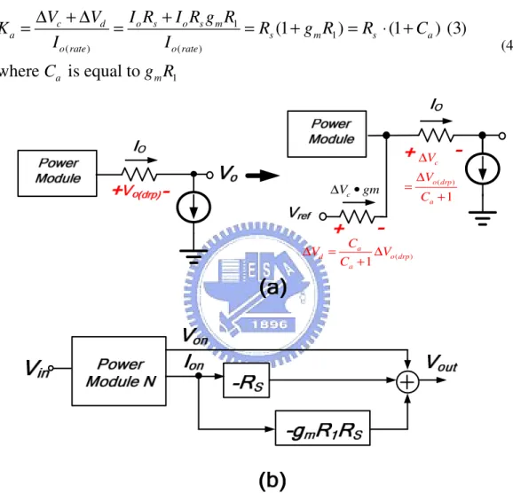
Fig. 8. Current sharing controller with DDS technique in single power module. ... 10
Fig. 9. Modified droop technique to reduce the power dissipation on sensing resistor Rs (a) Insertion of another sensing loop to conventional droop technique. (b) Flow diagram of new dual sensing loop of DDS technique ... 11
Fig. 10. Operation of DDS technique. ... 13
Fig. 11. Ca+1 raising voltage region for breaking through the limitation of conventional droop technique... 14
Fig. 12. Dynamic droop scaling technique in the ithpower module. ... 15
Fig. 13. Modified FVF technique in transconductor Gmto improve the linearity of transconductor. ... 15
Fig. 14. Schematic of circuit of incremental output voltage is composed of a current mirror, a current comparator array, and a adder of raising current. ... 16
Fig. 15. Using DDS technique in buck converter ... 18
Fig. 16. The sharp output voltage to load current waveform. ... 20
Fig. 17. The waveform of output voltage for different design in compensation region ... 21
Fig. 18. The theorist PNC waveform for voltage compensation. ... 22
Fig. 19. The analysis for using PNC method for single buck converter. ... 23
Fig. 20. the composed triangle waveform in PNC method ... 25
Fig. 21. The analysis for two parallel connected buck converters system ... 27
Fig. 22. The analysis for two parallel connected buck converters system ... 30
Fig. 23. The analysis for two parallel connected buck converters system ... 31
Fig. 24. The analysis for two parallel connected buck converters system ... 32
Fig. 25. The analysis for two parallel connected buck converters system ... 34
Fig. 26. The Whole circuit block diagram. ... 37
Fig. 27.the block diagram of the transconductor part. ... 38
Fig. 29. The simulation result of the bias current generation circuit ... 39
Fig. 30. The FFVF transconductor. ... 41
Fig. 31. The simulation result of the FFVF transconductor. ... 42
Fig. 32. The PNC circuit block diagram ... 43
Fig. 33. The winner take all circuit ... 44
Fig. 34. The simulation result for WTA circuit ... 45
Fig. 35. The current comparator circuit ... 46
Fig. 36. The simulation result for current comparator in (a) without hysteresis current (b) with 0.1uA hysteresis current ... 48
Fig. 37. The circuit implementation of the PNC current generator ... 49
Fig. 38. The Id current generator ... 50
Fig. 39. The Id current generator ... 51
Fig. 40. The SLC part block diagram. ... 52
Fig. 41. The operation principle of the FVC circuit. ... 53
Fig. 42. The pulse generator circuit ... 54
Fig. 43. The circuit implementation of the FVC circuit ... 55
Fig. 44. The simulation result of the pulse generator ... 55
Fig. 45. The simulation result of the FVC circuit ... 56
Fig. 46. The circuit implementation of the FIC circuit ... 57
Fig. 47. The circuit implementation of the V to I converter ... 58
Fig. 48. The simulation result of the output current ISLC of FIC circuit in different operation frequency for (a) 5V supply voltage (b) 3.3V supply voltage ... 59
Fig. 49. (a) the logic circuit (b) the flow chart of the logic circuit ... 60
Fig. 50. The simulation result of the voltage and current waveform for paralleling system with IDDS technique ... 62
Fig. 51. The simulation result of the current waveform during the transition between two modules. ... 62
Fig. 52. The model of the measurement environment ... 64
Fig. 53. (a)the measured current waveform (b) corresponding PWM signal ... 65
Fig. 54. The measured output voltage waveform ... 66
Fig. 55. The compare of the efficiency between single and paralleled buck converters in (a) VDIN=3.3V fIN =500kHz (b) VDIN=5V fIN =5MHz. ... 68
Table Captions
TABLE I the Boolean value of the control signals ... 50 TABLE II the output current of the ISLC current in corresponding conditions ... 66
Chapter 1
Introduction
The increasing demand of green energy in today’s electronic devices needs multiple input sources to deliver high driving capability to single output. Thus, parallel DC-DC converters are widely used to achieve large driving capability. That is, the paralleling of DC-DC converter modules offers a number of advantages over a single centralized power supply. This thesis introduces the benefit of using multiple-input source single-output (MISO) system in Chapter 1.1 first. Second, when several DC-DC converters are connected in parallel, the major concern is the uniform current distribution of each converter. Two kinds of current sharing methods with different complexity and current-sharing performance are introduced in Chapter 1.2. In Chapter 1.3, the discussion of the conduction and switching losses at different loading condition is described to find out a better way for the power management control for parallel DC-DC converters.
1.1 The benefit about multiple input source
single output (MISO) system
With the explosion development of integrated circuit, the consumer specification of the power system is hard to meet only by means of single power system. Therefore, the MISOsystem is utilized to satisfy the requirement in Fig 1.
The advantages of the MISO systems are as follows [1]. The first advantage is modeled power system. Using single power system, the designer needs to redesign the whole system when the consumer requirement is changed. However, the MISO system has the parallel modeled power system and the output power requirement can be met by just choosing the number of parallel power system modules. The second advantage is high current driving capabilities. That is, the load current of the MISO system is separated into multiple power system, thus lowers the requirement of the current driving capability for single module. The third advantage is high conversion efficiency. The power efficiency for the MISO system is better than that of the single power system since the conduction loss is greatly reduced by means of parallel connected power system [2].
1.2 The introduction for two majorly current
sharing methods
When the MISO system is used, if the current-sharing mechanism of the Fig. 1. MISO system.
converter system is not well-designed, one or more modules may bear higher load current. As a result, the reliability of the system is deteriorated and the merit of paralleled power supplies is as significant as expected. In this section, a brief introduction for two types of most common current sharing methods, which are the droop and active current-sharing methods, is presented in this section.
1.2.1 Droop Method
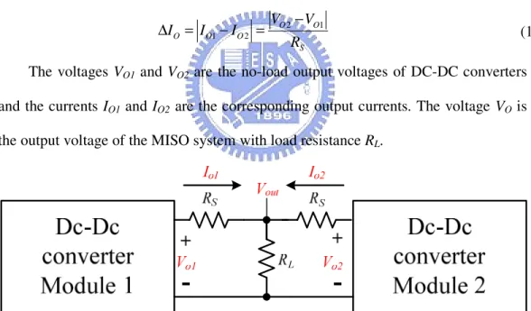
The principle of the droop method is to use the output resistance to form the function of current sharing [3]. In Fig 2, when the resistor RS is connected to the output of the DC-DC converter, the current difference ∆IO can be drive as (1).
2 1 1 2 O O O O O S V V I I I R − ∆ = − = (1)
The voltages VO1 and VO2 are the no-load output voltages of DC-DC converters and the currents IO1 and IO2 are the corresponding output currents. The voltage VO is the output voltage of the MISO system with load resistance RL.
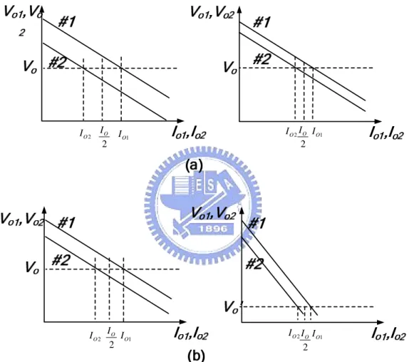
The current sharing performance affected by no-load output voltage of DC-DC converters is shown in Fig 3(a). If the difference between VO1 and VO2 becomes smaller, the current difference is decreased too. In Fig. 3(b), a larger resistor RS results in a better current sharing performance, but the output voltage will drop to a lower level if the same rated current is required, even that the value may be below the
minimum allowable output voltage. Since the no-load output voltage of DC-DC converters can not be decided by user and will be easily affected by the process variation of the components. Thus, the droop slope is the reasonable way and the trade-off between the current sharing performance and output voltage variation becomes the major concern using the droop method.
1.2.2 Active Current-Sharing Method
The major difference between the active current-sharing method and the droop method is the demand of an external pin to connect the current sharing bus as shown in Fig. 4. The current sharing bus conveys the output current information and provides
2 O I 1 O I IO1 2 O I IO2 2 O I 1 O I IO1 2 O I IO2 2 O I 2 O I
Fig. 3. The current sharing performance of droop method at (a) different output voltage for converters with no-load current and (b) different output voltage droop slope.
the signal for the internal current sharing controller to adjust the output current among all the power modules [4].
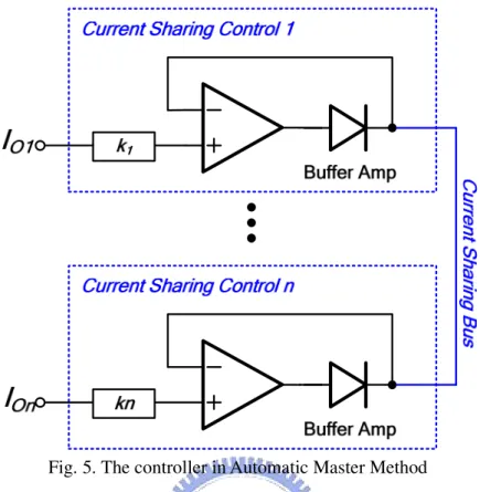
The automatic master method is the common technique using the internal controller for active current-sharing method [5]. The output current information of each power module is connected to the current sharing bus by a buffer amplifier with cascading a diode for rectifying the direction of current. Thus, it forces the current signal at current sharing bus is the highest output current and all the power modules can refer to this signal to adjust itself output current. The controller used automatic master method is shown in Fig 5.
The advantages about using the Droop Method compared with Active Current Sharing Method [6] are: The circuit is simple and easy to extend. It doesn’t need additional pin to connect with each power modules. The power system is easy to be modeled. The drawbacks are: The output voltage variation is increasing when larger droop slope is used. The current sharing performance will be limited by the minimum output voltage.
The advantages are superior to those of the active current sharing method. But the trade-off between the output voltage variations and current sharing performance by means of conventional method limits the popularity of droop method. It causes the designers to find a method to break through the limitation.
1.2.3 Paralleling control of power system
As we know, the conduction loss is larger than the switching loss at heavy loads [7]. It means that the parallel modules are suitable for improving conversion
efficiency owing to the small conduction loss. On other hand, at light loads, the parallel modules will consumes much power than single supply module due to the large switching loss. Especially, for the power system with large-size power MOSFET, the switching loss is huge at very light loads. Thus, for a well-designed parallel system, it must contain the ability to decide how many power modules are needed to supply the output load based on the current load condition. Therefore, the parallel control system needs a switching loss calculation circuit to decide when the parallel modules have the best conversion efficiency in case of load variations. The switching loss calculation (SLC) circuit is used to implement the mechanism of power management system as illustrated in Fig. 6.
These power modules can be supplied from different sources like NiH, NiCd, and Li-ion batteries or solar cells. Besides, the switching frequencies of the DC-DC converters can be different to each other. Due to the SLC circuit, the parallel control system can decide how many paralleling power modules are needed to drive the output load. Certainly, the input sources can have different voltage values and switching frequencies. In other words, the flexibility is effectively enhanced
Chapter 2
The Dynamic Droop Scaling
Method
According to the previous discussion, the prior art of dynamic droop scaling (DDS) method is presented to break through the limitation of conventional droop method. The limitation of conventional droop method is described in section 2.1 and the DDS method is proposed in section 2.2. In section 2.3, the implementation of the DDS technique is presented. The voltage variation problem when using the DDS technique is discussed in 2.4.
2.1
Limitation of Conventional Droop Method
Two major parameters are the value of difference voltage (ΔVo(set)) of DC-DC converters at no load and the value of droop slope K when we adapt conventional droop method in parallel systems. The former is the variations between different power supply modules. The tolerance of ΔVo(set) is usually controlled within ±1% value of output set-voltage Vo(set) in specification. Fig. 7 shows the relationship for output current and voltage of the droop method. In Fig. 7(a), the design margin for droop method is limited to ΔVo(drp), which is written as equation (2).
( ) ( ) (max) ( )
o drp o rate o o set
V
I
K
V
V
2
OI
IO1 2 O IFig. 7. Definition of dropout voltage.
Io(rate) is rated current load, ΔVo(max) is maximum allowable output voltage variation of the DC-DC converter systems. From Fig. 7(b), the maximum current deviation between two power supply modules is inversely proportional to the value of
K and can be driving as equation (3).
( ) 1 2 o set o o o
V
I
I
I
K
∆
∆
=
−
=
(3)It means that the larger value of K is, the smaller deviation between two power supply modules is. However, owing to the steeper slope of droop method, the voltage variation will exceed the minimum allowable output value Vo(min) at rated current load. In other words, there is trade-off between error percentage of current sharing and output voltage variation.
2.2 Dynamic Droop Scaling Technique
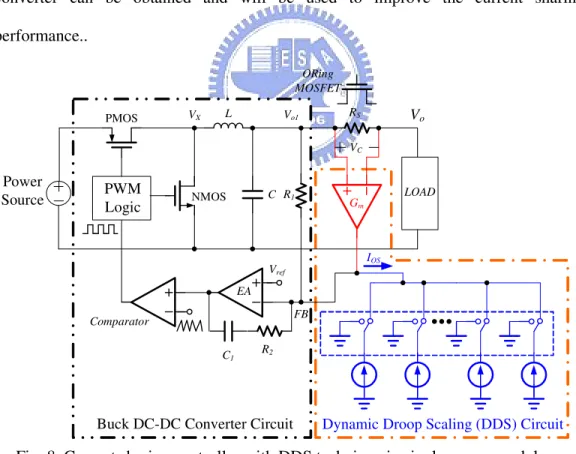
The major problem of conventional droop method is the limitation of the value of droop slope. Thus, dynamic droop scaling (DDS) circuit shown in Fig. 8 is added to the output of converters to exceed the limitation of conventional droop method [8]. The external resistor is composed of the on-resistance of ORing MOSFET [9], which is used to prevent the individual power supply module from burning out because of short circuit. The increment of load current increases the value of ΔVC by flowing
through the Rds(on) of ORing MOSFET, and therefore the output current of
transconductor Gm also increases. Thus, the load current condition of the DC-DC converter can be obtained and will be used to improve the current sharing performance..
PWM Logic
Dynamic Droop Scaling (DDS) Circuit
IOS Gm VC Vo RS Vo1 C LOAD EA Comparator Power Source PMOS NMOS L VX Vref C1 R2 R1 FB
Buck DC-DC Converter Circuit
ORing MOSFET
Fig. 8. Current sharing controller with DDS technique in single power module.
2.2.1 Principle of Dual Current Sensing Loop
amplifier is close to the value of Vref, and the current generated by transconductor will only flows through resistor R1 to generate a voltage drop, which is equal to ΔVd. The total voltage drop due to the increment of load current is the sum ofΔVC andΔVd. In Fig. 9(a), we can write the new droop slope Ka as equation (4):
1 1 ( ) ( ) 1
(1
)
(1
) (3)
where
is equal to
c d o s o s m a s m s a o rate o rate a mV
V
I R
I R g R
K
R
g R
R
C
I
I
C
g R
∆
+ ∆
+
=
=
=
+
=
⋅
+
(4) ( ) 1 c o drp a V V C ∆ ∆ = + ( ) 1 a d o drp a C V V C ∆ = ∆ + c V gm ∆ •Fig. 9. Modified droop technique to reduce the power dissipation on sensing resistor Rs (a) Insertion of another sensing loop to conventional droop technique. (b) Flow
diagram of new dual sensing loop of DDS technique
Fig. 9(b) shows the flow chart of dual sensing loop. It means that the value of new droop slope is (1+Ca) times of conventional droop slope and the variations of
Rds(on) values for different ORing MOSFETs can be compensated by the term of gmR1 in equation (4). We don’t need to put much effort on selecting the perfect matching external components for whole multiple-supplies system. Furthermore, owing to the
larger value of droop slope Ka, the error percentage of current-sharing performance is reduced by a factor (1+Ca). ( ) ( ) ( ) max
(1
)
o set o set o a aV
V
I
K
K
C
∆
∆
∆
=
=
⋅
+
(5)Compared with conventional droop method, the DDS technique consumes less power because only ΔVo(drp)/(Ca+1) is dissipated by ORing MOSFET. The rest voltage drop [ΔVo(drp)Ca/(Ca+1)] is dissipated by resistor R1. Fortunately, the current flowing through resistor R1 is only IoRsgm, which is far smaller than Io.
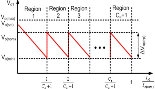
2.2.2 Incremental Output Voltage Loop
Generally speaking, the enhanced droop slope Ka deteriorates the minimum allowable output voltage at rated load current as shown in Fig. 10(a). Therefore, in order to keep output voltage of DC-DC converters within the range of minimum allowable output voltage and maximum allowable rated current, it is needed to raise the output voltage aboutΔVo(drp) for every Io(rate)/(Ca+1) current increment of output current. In Fig. 10(b), when the load current transits from region I to II, we raise the output voltage about ΔVo(drp) to meet the specification. Equation (6) and (7) describe the operation between two regions.
( )
1
where
(
1)
o ref o a o o rate aV
V
I
K
I
I
C
=
−
⋅
<
⋅
+
(6) ( ) ( ) ( )1
2
where
(
1)
(
1)
o ref o drp o a o rate o o rate
a a
V
V
V
I K
I
I
I
C
C
=
+ ∆
−
⋅
<
<
⋅
(a)
(b)
I
oV
o Slope=K ∆Vo(drp) (Ca+1)VO(drp) Slope= Ka=K(Ca+1)I
oV
o ∆Vo(drp) ( ) 1 o rate a I C + ( ) 2 1 o rate a I C + Region I Region II ( ) 1 o rate a I C + o rate( ) I Region N ( ) ( 1) 1 o rate a N I C − + ( ) 1 o rate a NI C +V
o(min)V
o(min)Fig. 10. Operation of DDS technique.
By extending two raising regions to Ca+1 raising regions according to the new drop slope, the load current and output voltage V-I waveform is shown in Fig. 11. Owing to the compensation for extra voltage drop of Ca+1 raising region, the droop scale can be increasing to (Ca+1) times of original and the error percentage of current-sharing performance can be shrunk to only 1/(Ca+1) times that of the conventional droop method.
Fig. 11. Ca+1 raising voltage region for breaking through the limitation of conventional droop technique.
2.3 The Implementation of DDS Technique
The implementation of dynamic droop scaling technique is composed of the high linearity transconductor and the incremental output voltage circuit. High linearity transconductor defines low power dissipation performance of droop technique and the circuit of incremental output voltage will break through the limitation of conventional droop technique.
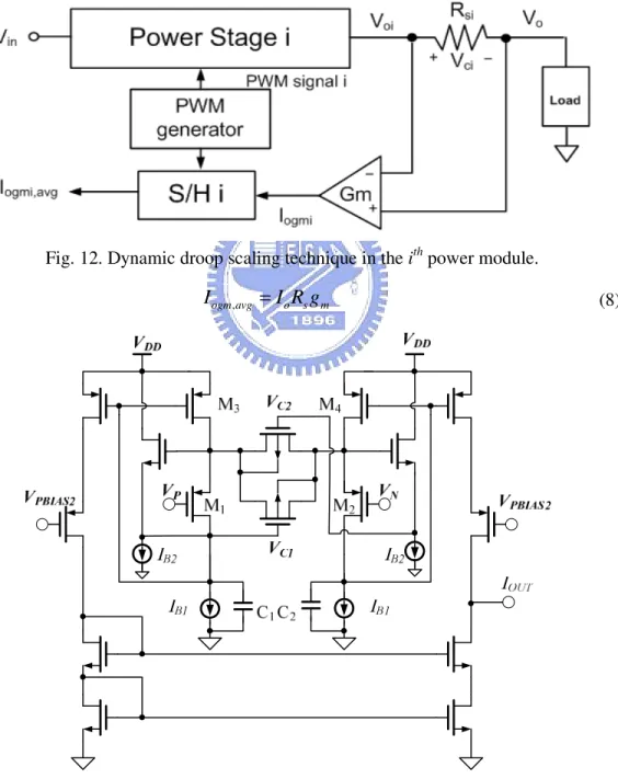
2.3.1 High Linearity Transconductor
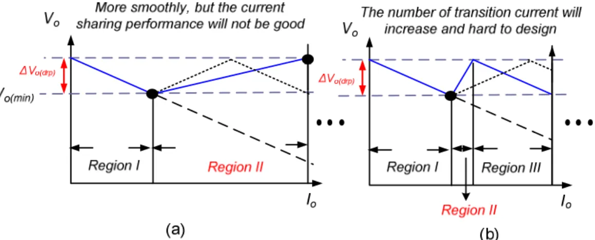
The linearity of transconductor is important in dynamic droop scaling technique. In Fig. 12, the output current of transconductor decides the droop slope of every power
supply module. Thus, for the system with the ith power module shown in Fig. 12, the
linearity of transconductor decides the error current among these supply modules. In order to improve the linearity of the transconductor, the flipped voltage follower (FVF)
[10] technique is used to reduce the output impedance. In Fig. 13, input differential pairs are composed of flipped voltage follower pairs, which are (M1, M3) and (M2, M4).
It means that the linearity of the transconductor can be improved by the characteristic of low output impedance of FVF. Furthermore, after the conversion of transconductor
Gm, S/H circuit samples the load current every switching period and hold this value as
Iogm,avg, which is written as equation (7) and shown in Fig.12.
Fig. 12. Dynamic droop scaling technique in the ithpower module.
Fig. 13. Modified FVF technique in transconductor Gm.
,
ogm avg o s m
The average current Iogm,avg is mirrored to two current branches. One is sent to error amplifier for the operation of droop method in Fig. 8. The other one is sent to incremental output circuit to decide the operating region.
2.3.2 Circuit of Incremental Output Voltage
Fig. 14 shows the circuit of incremental output voltage, which contains a current mirror, a smite trigger to be the current comparator array, and an adder of raising
current. The average current Iogm,avg sampled from output current of DC-DC converter
is sent to compare with reference current sources from 1/(Ca+1)IREF to Ca/(Ca+1)IREF to determine the increment current Ios. The raising current Iosflows through resistor R1 in Fig. 8 to generate constant voltage drop ΔVo(drp), and therefore provides the extra
compensation voltage ΔVos at the transition point of Ca+1 raising regions. The value of ΔVos relies on the new drop slope as equation (9):
( )
(
1)
OS o drp aV
V
C
∆
= ∆
⋅
+
(9) Iogm,avg Current Mirror 1/(Ca+1)IREF IOS VDD VDD VDD S/H Circuit Gm VC IogmCurrent comparator array Adder of raising current
Ca/(Ca+1)IREF SWCa IOSCa VDD VDD IOSb Switch 1 SW1 Switch Ca IOS1
Fig. 14. Schematic of circuit of incremental output voltage is composed of a current mirror, a current comparator array, and a adder of raising current.
For example, the new droop scale is set to Ca times the value resulted form the conventional method, offset current source is composed of Ca identical current sources from Ios1to IosCa. As the result, the decision codes (SW1~SWCa) will be sent to current mirror array with a sequence. The switches from switch 1 to switch Ca are turned on according to the operating region decided by Iogm,avg which is proportional to the output current of DC-DC converters. In other words, the larger the load current is, the more switches are turned on and the output voltage will be compensate with moreΔVos. Owing to the implementation of incremental output voltage circuit, the output voltage will not exceed the allowable minimum output voltage at rated load current.
2.4 The voltage variation problem when using the
DDS technique
Because of the reference voltage of error amplifier internal of the DC-DC converter can not be obtained while using DDS technique, using the feedback loop of the converters to adjust the output voltage for doing current sharing work is the better way. Taking the buck converter to be example, Fig. 15 shows the implementation of using the DDS technique to do the current sharing. For RFB1 and RFB2 is the feedback resistance of the buck converter, the feedback voltage will be regulated by internal error amplifier to Vref [11] which is generated by the bandgap circuit in buck converters when the system is in steady state. Where Vref can be calculated as:
2 ( ) 1 2 FB ref FB o set FB FB
R
V
V
V
R
R
=
=
+
(10)The droop enhancement current Iogm will source to the feedback pin of buck converter making the current that flow through the RFB1 decrease and provide the
additional voltage drop to output voltage of buck converter.
FB ref
V
=
V
Fig. 15. Using DDS technique in buck converter
And the compensate current IOS will sink from the feedback pin providing theΔ
Vos voltage raise to output voltage. In other words, the VFB and the RFB1 will be the Vref and R1 in Fig. 8. A stability problem is needed to be mentioned when the DDS
technique is used to a DC-DC converter. Because of any small distribution at feedback pin makes the converter having transition response, the sharp dc current change cause by the incremental output voltage circuit in Fig. 11 will produce a DC voltage drop at feedback pin and make the system into transition state [12]. If the output current of the DC-DC converters change rapidly and widely, the system will keep taking transition response and make the output voltage to have variation problem. The variation of the output voltage can be huge according to the transition performance of DC-DC converters and the current change of incremental output voltage circuit, that will effect the current sharing performance and need to be improved by finding a better way to compensate the output voltage drop by the DDS technique.
Chapter 3
The theory of PNC method and
SLC circuit
From the discussion in Chapter above, there is two problem need to be concern about. In Chapter 1, the switching loss problem at light load condition for parallel converters has been point out that need to find a dynamic control method to improve light load efficiency. And in Chapter 2, the output voltage variation problem needs to be deal with when the DDS method is using to enhance the droop slope for better current sharing performance. The positive/negative compensate (PNC) method will be introduced in Chapter 3.1 to make the compensate current of incremental output voltage transit smoothly, reduce the output voltage variation. And the analysis about using PNC method on buck converters will be presented in Chapter 3.2. In Chapter 3.3, the loss analysis on a modeled buck converter will be introduced. Finally, the theory about switching loss calculation (SLC) circuit will be presented to provide a really good method improving the efficiency of the parallel buck converters at light load condition in Chapter 3.4.
3.1 The theory about positive/negative
compensate (PNC) method for voltage
compensate circuit
In the DDS, the steeper droop slope has a better current sharing performance due to the large droop resistor. However, the voltage variation may exceed the allowable minimum output value Vo(min) at rated current load Io(rate) as depicted since the large voltage drop across the large droop resistor. In other words, there is a trade-off between the error percentage of current sharing and the output voltage variation. Thus, the voltage incremental circuit is involved in the DDS technique to break through this limit. As shown in Fig. 16(a), the conventional method in DDS has two major drawbacks. The output voltage at the transition currents will be undefined causing the stability problem and the sharp waveform deterioration the output voltage variation problem decreasing the current sharing performance.
V
o ∆Vo(drp) ( ) 1 * 1 o rate a I C + ( ) 2 * 1 o rate a I C + Region I Region II The voltage at these current will be undefinedWaveform is sharp
I
oV
o(min)To solve this problem, the compensation method should not only add a DC voltage raise to the output voltage when it drop to Vo(min) during the output current increasing. In order to smooth waveform, the compensation voltage can not be raised instantly and a compensation region should be created. The variation of the output voltage near the transition current need to decrease as much as possible, it means the condition of output current must be considered for being a element of the compensate voltage. Since the Vo(min) is reached, using the positive droop slope for compensation region of output waveform is the only way. While designing the compensation region, we still need to mention that the slope of waveform effect the current sharing performance directly. Fig. 17 show the waveform of different design of output voltage, the even region is compensation region. In Fig. 17(a), smaller compensation slope of the output voltage smooth the waveform but the current sharing performance be worse than original. With bigger slope in Fig. 17(b), the number of transition current is increased due to more regions are created and the circuit design difficultly is increased. At the same time, the current sharing performance will not be same in different region causing the stability problem.
Fig. 17. The waveform of output voltage for different design in compensation region (a) smaller slope (b) bigger slope
Thus, the improved DDS (IDDS) technique with the new positive-negative compensation (PNC) method is presented in Fig. 18. According to the PNC method, the rated current is divided into Ca+1 regions within the allowable output voltage variations and the transition current keep the same with original DDS technique by just
turning the even region in Fig. 10.(b) to be the compensation region. The slope Kaof
each odd region is – ∆Vo(drp)(Ca+1)/ Io(rate). On other hand, each even region has a slope of ∆Vo(drp)(Ca+1)/ Io(rate) where Ca is the magnification factor for increasing the droop slope in the DDS technique.
( )
(
1) /
( )for Reigon I, III, V...
a o drp a o rate
K
= −∆
V
C
+
I
(11)( )
(
1) /
( )for Reigon II, IV, VI...
a o drp a o rate
K
= ∆
V
C
+
I
(12)The transition from two different regions causes the droop slope has different signs in order not to exceed the allowable output voltage variations. And the slope in compensation region is same with the original droop enhanced by DDS to keep the
I
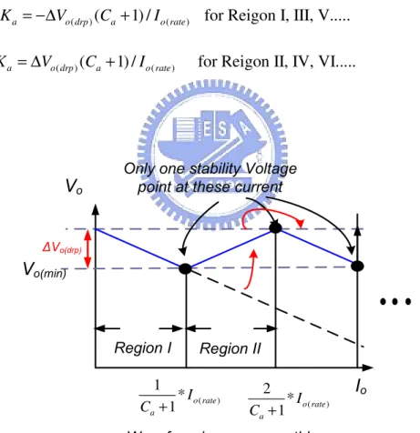
oV
o ∆Vo(drp) ( ) 1 * 1 o rate a I C + ( ) 2 * 1 o rate a I C + Region I Region IIOnly one stability Voltage point at these current
Waveform is more smoothly
V
o(min)current sharing performance. Certainly, the IDDS technique has a more stable operation than the previous DDS technique due to the smooth transition between two different regions. It can extend the rated current load within the allowable output voltage variations and will not cause the output voltage variation problem.
3.2 Analysis for using PNC method for buck
converters
Take buck converters to be example, the discussion can be divided into two parts as analysis for single buck converter and analysis for parallel buck converters.
3.2.1 Analysis of single buck converter
Continued from the previous discuss in Chapter 2.4, let us consider the saturation for single buck converter first. Using the PNC method for buck converter can be analyzed in Fig. 19
R1 and R2 are the feedback resistors of the buck converter. Because the VFB is regulated to Vref by the internal circuit in the buck converter, the current I1 and the
original output voltage Vo(set) can be calculated by let I2=I1 as follow [13]:
2 ( ) 2 1 2
,
ref o set refV
I
V
V
I R
R
=
=
+
(13)For Rsis the Rds(on) of the ORing MOSFET providing the original droop slope, Io is the output current of the converter, the current Iogm is the current shown in equation (8) which is generated by the transconductor in DDS circuit and the current IPNC is the droop enhancement current from IDDS circuit mixed with the compensation current
Icom and Iogm. The new output voltage Vo of buck converter can be derived as follow:
1 1
o ref
V
=
V
+
I R
(14)Since the FB pin of buck converters will not sinking or sourcing current from VFB
and the current I2 is regulated at stately state as equation (13), I1 can be calculated from equation(15):
2 1 PNC
I
=
I
+
I
(15)If the IPNC is positive meaning the current is sourcing to the VFB pin, the current I1 will be lesser than I2 resulting in the Vo<Vo(set) from the comparison with equation (13) and (14), and if it is negative meaning the current is sinking from the VFB pin, the
Vo>Vo(set) will be the result. Consider saturation that the current IPNC is increasing, the output voltage waveform will get a negative slope because of the decreasing current of
I1. On the other hand if the IPNC is decreasing, the output voltage waveform will have a positive slope due to the increasing value of I1.
It seems that the current IPNC is the key elemental of the PNC method and the design of IPNC is most important part overall. The analysis of IPNC is shown in Fig. 20.
VoL(set), the maximum voltage drop range is ΔVoL(drp) and the rate current is IoL(rate) with the output current of IogmL from the transconductor in IDDS. For (Ca+1) times enhancement from original droop slope, the rate current is separated into (Ca+1) Region and need to be compensated due to additional voltage drop. The waveform of
V+IgmL is produced by sinking the current I+gmL which is proportional to IogmL from VFB
pin. Otherwise sourcing the current I-gmL being proportional to IogmL to the VFB pin will
generate the waveform of V-IgmL. The triangle waveform that is the final result in PNC
method can be composed with taking part of waveform in V-IgmL and V+IgmL. But there
are still two major concern need to be deal with, the voltage drop at the on-resistance
of ORing MOSFET Rs and the DC voltage difference.
Let us consider the (Ca+1) times enhancement droop slope in DDS, the Ca times
voltage drop is provided by controlling the current I1 and the original one times slope is provided by the Rs. If the positive (Ca+1) times slope is need, the current I1must produce (Ca+2) times slope by flowing through the R1to overcome the original slope.
From the discussion above, the current I-gmL andI+gmL will have the relationship as follow:
, where k is a constant
gmL ogmLI
+=
kI
(16)2
a gmL gmL aC
I
I
C
+ −+
=
(17)The other problem comes from the DC voltage difference from the waveform of
V-IgmL and V+IgmL. Although the positive and negative slope can be composed by the waveform of V-IgmL and V+IgmL but a compensation voltage Vcomis required to shift the DC voltage level at transition currents to make the continued triangle waveform. Since the voltage drop in every region isΔVoL(drp), the compensation voltage Vcom can be calculated at different transition currents in Fig. 20 as follow:
( )
2
, where
for region N
2
com oL drp
N
V
=
nV
n
=
(18)This compensation voltage can be generated by adding a current IcomL to flow through the R1 additional to I+gmL or I-gmL. Finally, the compensation current IPNCL that can produce the triangle waveform for a single buck converter can be derived in equation (18), (19). 1
1
Nfor region N
PNCL gmL comI
= −
−I
+
I
(19) ( ) 10 for region 1
2
, where
-1 for region N
2
comL oL drp N comLI
V
N
I
R
σ
σ
=
∆
=
•
•
=
(20)3.2.2 Analysis for parallel buck converters
For the parallel buck converters system, we need to consider the synchronization problem. If all of the buck converters are not operated in positive region or negative region at the same time, the output voltage difference between each buck converters will increase and deterioration the current sharing performance. Thus the better way to control the whole system is transiting all the parallel buck converters at the same time. Otherwise the compensation current IcomL for each buck converters will be different according to the original output voltage at no load condition and the DC voltage level at transition currents. Thus it is arduous to design the fixed particular current IcomL by sensing the initial condition for each buck converter. There must be another way to compensate the DC voltage difference for each buck converters additional to the current in equation (19) for parallel buck converters system.
Let us simplify the question by taking 2 buck converters to be example in Fig. 21.
V c o m V com comV n V c om n V c om ( ) Lo drp I
V
( )/(
1)
oL rateI
Ca +
( )2
com oL drpV
=
V
22
∆
V
d=
2(
V
+Igm−
V
+IgmL)
V c o m Vc o m Vc o m V c o m ’Fig. 21.show the analysis for two buck converters system: Buck 2 and Buck L, where Buck L is the buck converter with lowest original voltage output at no load current condition and Buck 2 is one of the buck converters other than Buck L.
There are many reasons for making the transition current decided by Buck L. Because of the original output voltage of it is lowest at no load condition in each buck converter, theΔVo(drp) of it is the smallest one resulting in the Rs value which provide the original slope can not be too large. In other words, it is the worst case from all parallel buck converters. Due to the VoL(set) is the smallest output voltage, the output current of Buck L will be the lowest and since the output current of each buck converter is sampling from the transconductor to Iogm, it is possible to find the lowest one. By setting the IoL(rate) of Buck L to be the condition for transition current, the
IoL(rate)/(Ca+1) will be the range between each transition current and the 2VoL(set)will be the compensation voltage Vcom.
For the Buck 2, because of the total DC difference voltage will change according to the initial voltage of the buck converter. From the analysis in Fig. 21, in order to generate the continued triangle output voltage waveform, we can find the compensation voltage drop when using V+Igm2 to provide positive slope can easily be obtain by adding 2 times of voltage difference between V+Igm2and V+IgmLadditional to
Vcom. Thus, an additional voltage drop 2ΔVd is generated by sourcing a current proportional to the current difference Id through the R1, where:
2
-d ogm ogmL
I
=
I
I
(21)2 2 1 1
2
∆
V
d=
2(
V
+Igm−
V
+IgmL)
=
2(
I
+gm−
I
+gmL)
R
=
2
kI R
d (22)The compensation voltage drop 2ΔVd only need to be added when transit into even region with positive slope to Buck 2. The stability may be challenged in parallel buck converters system by letting the buck converter with larger output current
compensate more voltage than lower output current one in positive slope region, but the solution is obviously. The compensation voltage 2ΔVd drop also providing the negative feedback loop for stability during positive slope region, if some perturbation
occur to increase the current difference between Buck 2 and Buck L, theΔVd for will
increase providing additional voltage drop at Buck 2, reducing the output voltage difference between Buck 2 and Buck L, force the current difference back to the setting of IDDS.
According to the principle discuss above, the operation when M number of parallel connected buck system can be obtain. Sampling the current output from the
transconductor and choose the buck converter with lowest Iogm current to be the Buck
L first. Setting the IoL(rate) to decide the transition current and calculate the current difference between IogmN to IogmL is the second part. Finally, an index of the IPNCM for Buck M except than Buck L can be drive as follow:
1
1
Nfor region N
PNCM gmM comMI
= −
−I
+
I
(23) ( ) 10 for region 1
2
(
1) , where
-1 for region N
2
comM oL drp N comM dI
V
N
I
k
I
R
σ
σ
σ
=
∆
=
•
•
+
+
=
(24)The mathematic formula of IPNCM and IPNCL may be complex, but the circuit for PNC method is quite simple making it is easy to implement.
The analysis above proving the PNC method with lesser output voltage variation by output the continued triangle voltage waveform, and the stability in positive slope region can be maintained from the current difference element Id in total output current
IPNC of IDDS circuit. The PNC method using by IDDS is really better than the original compensation circuit in DDS.
3.3 The loss analysis on a modeled buck
converter
From the discussion in Chapter 1.2.3, a power management system is needed to improving the light load efficiency of parallel buck converters due to the switching loss. To design the whole power management method, we need to analysis the loss when a buck converter is supplying the energy.
Start from modeling the buck converter in Fig. 22 first. Because of the output current for the buck converter is several ampere in our case, the power MOSFET is always external the buck converter due to the huge size. An external high current specification power MOSFET result in huge input capacitor and make the high side MOSFET using NMOS rather than PMOS because of the current driving density of NMOS is better than PMOS [14].
Vo
M
NP1M
NP2BUCK
conduction loss part
M
ORR
sR
LDCRR
ds(on)R
ds(on)switching loss part
C
pC
pLet the discussion focused on the external conduction loss and switching loss and for the value of the output current Iout is several ampere, thereby ignoring the internal loss of each buck converter. Since the conduction loss occurs on the current path mainly [15] and the switching loss occurs on the power MOSFET [16], the model of buck converter in Fig. 22 can be separated into conduction loss part and switching loss part. The resistance on current path is shown in figure, VDIN is the supply voltage and the on-resistance of ORing MOS using to provide the slope in IDDS is Rs, the RLDCR is the DC equivalent resistance of inductor and the on-resistance of power MOSFET is
Rds(on). For the output current Iout, the loss on the power MOSFET is DIout2Rds(on) and
(1-D)Iout2Rds(on) due to the switching operation of buck converter [17]. The power loss on conduction loss part is shown in Fig. 23.
After summing the power loss on each device, the total conduction loss PCN can be calculated as follow: 2 ( ) ( ) PN out ds on LDCR s P =I R +R +R (25)
For the switching loss part, the switching frequency of buck converter and the
input capacitor Cp of power MOSFET is considered. The switching loss can be discuss
from the power MOSFET transition switching loss and the gate driving loss of power MOSFET which is shown in Fig. 24.
The power MOSFET transition switching loss is 0.5*(fINVDINIoutton+off), where ton+off is the summation time of the power MOSFET from off-to-on and on-to-off [18], it is proportion to current driving ability of the buffer stage internal the buck converter and the value of Cp. The gate driving loss can be calculated by the equation (26):
2
P
=
fCV
(26)Due to the NMOS type high side power MOSFET, the bootstrap technique is
needed for the source terminal of it being Vo but ground to get a good “1” when turn
on it [19]. The bootstrap technique pump up the gate voltage to about 2VDIN when turn on the high side power MOSFET, thus the gate driving loss on it is 0.5*fINCp(2VDIN)2.
The total switching loss PSW can be calculation as follow:
2
5
2
SW IN DIN out on off IN p DIN
P
=
f V
I t
++
f C V
(27)Due to the high output current specification and the huge input resistance of the external power MOSFER, the other loss can be ignored for the domination of these two types of power loss. The total power loss Pt1 can be simply to equation (28):
2 2
1 1 1 ( )
5
(
)
2
t SW PN out ds on LDCR s IN DIN out on off IN p DIN
P
=
P
+
P
=
I
R
+
R
+
R
+
f V
I t
++
f C V
(28)3.4 The theory about switching loss
calculation (SLC) circuit
The discussion on previous section shows the power loss on an operated buck converter. Within the help of these equations, the power management control method can be obtained by analyzing the power loss relationship between single and parallel connected buck converters. For the output current Iout, let us define using single buck converter to supply the energy to be the “single module” and using parallel connected buck converters to be the “parallel modules”. Fig. 25 shows the analysis of power loss on the N parallel modules. The only difference compare to the single modules is the output current for each buck converter is divided into 1/N times of Iout, thus the total power loss PtN is:
2
( ) 2
(
)
5
2
out ds on LDCR s
tN IN DIN out on off IN p DIN
I
R
R
R
N
P
f V
I t
f C V
N
++
+
=
+
+
(29)Comparing with the power loss in the single module, the value of PSWN, which is
the total switching loss of the N power modules, is n times that of gate driving loss part in PSW1 for a single power module. But the value of PCN1 in a single power module is n times that of PCNN, which is the total conduction loss of the N power modules. Since the switching loss depends on the switching frequency fIN not on IOUT. Thus, an incremental power module may increases more switching loss but decreases the conduction. The suitable addition of a power module can be derived by (30).
2 2 ( ) 5( 1) 1 2 IN p DIN SW CN outp ds on s LDCR N f C V N P P I R R R N − − ∆ = ∆ ⇒ = + + (30)
It means if the parallel current output is Ioutp, the total power loss Pt1 for supplying from single modules keep the same with the PtN in N parallel modules. In
MOR
V
OUTM
NP1M
NP2BUCK
(I
out/N)
2R
LDCR Module I Module II Module NV
DINswitching loss part
conduction loss part
(1-D)(I
out/N)
2R
ds(on)(I
out/N)
2R
sD(I
out/N)
2R
ds(on)½fINCP(2VDIN)
2½fINVDINIOUTton+off
½f
INC
PV
DIN2½f
INV
DINI
OUTt
on+offother words, if the output current Iout < Ioutp, the Pt1 will be lesser than PtN and using the single module to supply the output will be more efficiency. For the situation that Iout >
Ioutp, using the N parallel modules will be more efficiency. There is another improvement in single module. Because that the current sharing issue is not considered in single module, therefore the Rs can bescaled down to reduce the conduction loss of ORing MOSFET which is impossible for keeping the current sharing performance in parallel modules. Assuming that the paralleling system uses N paralleling ORing MOSFETs, the on-resistance of the ORing MOSFETs in single module will become
Rs/n and equations (31)-(32) can be derived.
2 2 ( )
5
1
[
]
2
IN p DIN outp ds on LDCRf C V
I
R
R
N
>
+
(31) ( )5
Poutp IN DIN C IN DIN
ds on LDCR
NC
I
f
V
K
f
V
R
R
=
•
•
=
•
+
(32)The current Ioutp will be the transition current between single module and paralleling modules. Because of the capacitance Cp, Rds(ON) and RLDCR only depend on the output current specification. Thus, in (32) a constant Kc is used to simplify the equation. Thus, Ioutp is proportional to the root of the fIN and VDIN, which are the parameters of the buck converters. It means that the transition current Ioutp must take some important parameters of buck converters condition into consideration and these parameters are also the major element for calculating the gate driving loss in switching loss part. Thus, a circuit with the ability to calculate the equation (32) named as switching loss calculation (SLC) circuit is proposed in this paper to be the core of the power management method for parallel connected power system.
Chapter 4
Circuit Implementations and
simulation result
In this chapter, we will give a design procedure of our improved DDS with PNC method and the power management method with SLC circuit. At first, Chapter 4.1 shows the whole circuit block diagram and describes the operation method for all function block. In Chapter 4.2, the transconductor part will be introduced, it contains the FFVF transconductor, the bias current generator and the sample and hold circuit. The PNC part will be shown in Chapter 4.3, the current comparator and the winner take all circuit used in it will be introduced too. The SLC circuit and the logic control part will be presented in Chapter 4.4. Finally, the whole circuit simulation is shown in Chapter 4.5. The design environment is TSMC .35 2P4M.
4.1 The whole circuit block diagram
The system can be divided into three major blocks, the transconductor part, the PNC method part and the SLC circuit. The whole circuit block diagram for using IDDS with SLC circuit at the buck converter is shown in Fig. 26, the output current information will be gathered first in the transconductor part first. A voltage drop Vc will be generated when the output current Iout flow through the ORing MOSFET and
the function of the GM part transmutes Vc to a current Igmhich is proportion to Iout. The PNC part will output a current IPNC to do the current sharing and voltage compensation work. The current IPNC is generated by mixing the transcundoctor current Igm and the compensation current Icom, and output it to the feedback pin of the buck converter. The SLC circuit will provide the power management control to the buck converter. It gathers the operation frequency and the supply voltage information of the buck converter to control the enable signal of buck converter and ORing MOSFET according to the transconductor current Igm. In this secession, the block diagram for all three function parts will be presented.
4.2 The circuit implementation of the
transconductor
Fig. 27 shows the block diagram of the transconductor part of the IDDS circuit. Fig. 26. The Whole circuit block diagram.
The bias circuit supply the bias current to all the function block, the FFVF transconductor transmute the Vc signal into a current Iogm which can be the output current information of the buck converter, and the sample & hold circuit is using to removed the effect form the noise and the phase difference between each buck converter making sure the current sharing performance not being effect by them.
4.2.1 The bias current generation circuit
Fig. 27.the block diagram of the transconductor part.
The bias current generation circuit is shown in Fig. 28 [20] [21], after the supply source VDD rising up, the MOSFET MS1 turn on pulling up the gate voltage of
MOSFET MS2 and MS3. It creates an initial current through the bias current generation
part and establishes the biasing point according to the Rb and the process parameters of MOSFET. The MOSFET MB1 and MB2 mirror out the biasing current to the other
circuit. In Fig. 29, the simulation result of the bias current generation circuit show the output biasing current IBP in different temperature conditions, the current has positive coefficient to temperature. This biasing current will be the current supply of almost all circuit in IDDS circuit.