Nanotechnology, National Sun Yat-Sen University, Taiwan d
Department of Photonics and Display Institute, National Chiao Tung University, Taiwan
The formation of germanium nanocrystals embedded in silicon-oxygen-nitride with distributed charge storage elements is pro-posed. A large memory window was observed due to isolated Ge nanocrystals in the SiON gate stack layer. The Ge nanocrystals were nucleated after a high-temperature oxidized SiGeN layer. The Ge nanocrystals embedded in the SiON stack layer exhibited nonvolatile memory characteristics with the obvious threshold voltage shift under a bidirectional voltage sweep. Also, the manu-facturing technology using the sequent high-temperature oxidation of the a-Si layer and the direct oxidation of the SiGeN layer is proposed, respectively, for the formation of a blocking oxide layer to enhance the performance of nonvolatile memory devices. The reliability characteristics, including retention time and endurance, are also advisable for the application of nonvolatile memory device.
© 2007 The Electrochemical Society. 关DOI: 10.1149/1.2717494兴 All rights reserved.
Manuscript submitted October 17, 2006; revised manuscript received January 15, 2007. Available electronically April 3, 2007.
In 1967, Kahng and Sze invented the floating-gate共FG兲 nonvola-tile semiconductor memory 共or flash memory兲 at Bell Labs.1 To date, the flash memory device structure continues to be the most prevailing nonvolatile-memory implementation, and is widely used in both standalone and embedded memories. Because of the low working voltage and nonvolatility, the selection of storage media for most portable electronic devices is the Flash memory which is closely based on the structure of the continuous FG.2In a conven-tional FG memory device, charge is stored in a poly-Si floating gate surrounded by dielectric. The most prominent problem with this is that once there is a charge leakage path共resulting from P/E-cycle degradation兲 in the gate oxide, all the charges stored in the floating gate will leak away from this one single path because charges are stored in continuous energy level共conduction band兲 in FG. There-fore, for mass production, there is a trade-off between speed and reliability for the optimal tunnel oxide thickness. Once a leaky path has been created in the tunnel oxide, all the charges stored in the floating gate will be lost. Therefore, several methods are proposed to overcome this oxide quality limit of the conventional FG structure.2-7To alleviate the scaling limitation of a conventional FG memory device while preserving the fundamental operating prin-ciple of memory, a distributed charge storage approach such as nanocrystal nonvolatile memory was proposed.5-7 Nanocrystal charge storage offers several advantages, the main one being the potential to use thinner oxide without sacrificing nonvolatility. Un-like the floating gate, stored charges in isolated nodes cannot easily redistribute among themselves and a local leaky path will not cause a fatal loss of information for the nanocrystal nonvolatile memory device. This effectively prevents the leakage of all the stored charges out of the floating gate. Also, the nanocrystal memory de-vice can maintain good retention characteristics and lower power consumption.
Nanocrystals within semiconductor materials have attracted par-ticular attention because of the possibility of integrating nanocrystal with novel or superior properties into existing nanoeletronic and optoelectronic technologies. Si and Ge nanocrystal memories have superior potential for pushing further the scaling limits of conven-tional nonvolatile memory.2 In this contribution, the nitride-incorporated silicon germanium共SiGeN兲 was proposed to be a self-assembling layer of Ge nanocrystals in our previous study.8 The
SiGeN layer was directly deposited using a plasma-enhanced chemi-cal vapor deposition共PECVD兲 system. After high-temperature ther-mal oxidation, the Ge nanocrystals were nucleated in the oxidized SiGeN layer. The conditions of thermally oxidized SiGeN layer were also discussed in this study. In addition, the electrical reliabil-ity for the proposed metal-oxide-insulator-oxide-silicon 共MOIOS兲 structure is investigated. Also, material analysis such as Fourier transform infrared spectroscopy共FTIR兲, transmission electron mi-croscopy共TEM兲, and Auger electron spectroscopy 共AES兲 were uti-lized to determine the composition and structure of the oxidized SiGeN film. The electrical characteristic analysis, including capacitance-voltage共C-V兲, current-voltage 共I-V兲, retention time, and endurance, were also performed.
Experimental
Figure 1 shows the process flow in this work. First, a 5 nm thick thermal oxide was grown as the tunnel oxide on a p-type Si substrate by dry oxidation in an atmospheric-pressure chemical vapor deposi-tion共APCVD兲 furnace. Subsequently, a 20 nm amorphous silicon germanium nitride layer was deposited by PECVD on the tunnel oxide. The precursors of SiH4 共20 sccm兲, GeH4 共5 sccm兲, NH3
共30 sccm兲, and N2共500 sccm兲 were fed into the PECVD chamber
to deposit the SiGeN film at 200°C at a low pressure of 0.6 mTorr with plasma radio-frequency共rf兲 power of 20 W. The low pressure of 0.6 mTorr during deposition leads the mean free path of electrons to be increased and improves the uniformity of the thin film. Next, the high-temperature SiGeN oxidation was performed in the thermal furnace under oxygen ambient. An oxidation process was then per-formed to fabricate the oxygen-incorporated SiO2, acting as a
block-ing oxide layer. The oxidation temperature was at 900°C for 30, 45, and 60 min, respectively. In this work, we also developed another technology for the blocking oxide formation to enhance memory
*Electrochemical Society Active Member.
z
E-mail: [email protected] Figure 1.共Color online兲 The process flow proposed in this work for direct
performance, except for the direct oxidation of SiGeN film. In this contribution, an a-Si layer was deposited additionally on SiGeN layer by PECVD at 200°C under a low pressure of 0.6 mTorr with precursors of SiH4共20 sccm兲 and H2共980 sccm兲 and plasma power
of 20 W. Then a subsequent high-temperature oxidation process was implemented to transfer the a-Si film into a blocking oxide layer. Finally, the Al gate was deposited and patterned on the blocking oxide layer formed by these two methods to fabricate a MOIOS structure with the charge trapping insulator of SiGeN.
Results and Discussion
Memory device with directly oxidized SiGeN as blocking oxide.— Figure 2 shows the FTIR analysis for the as-deposited SiGeN layer. The initial peak signals of Si–H, Ge–H, and N–H in the as-deposited SiGeN thin film are clearly found in the FTIR spec-trum. A thermal furnace process was introduced to form blocking oxide共SiON兲 and segregate Ge atoms in this study. During the dry oxidation process at 900°C, Si atoms in the SiGeN film more easily combine with O2to form a SiON layer than Ge atoms do. Because
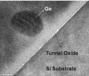
of the low solid solubility of Ge elements in silicon oxide, the Ge atoms will be segregated downward until they reach the tunnel oxide surface,9-11 and nucleate to form Ge nanocrystal near the tunnel oxide. Therefore, the SiGeN film will be oxidized to form SiON film as the blocking oxide; meanwhile, the Ge nanocrystals segregated in the SiGeN film and were embedded in SiON dielectric near the tunnel oxide. The TEM analysis and the Raman analysis support the point of view, as shown in Fig. 3 and 4, respectively. It is clearly found that Ge nanocrystals were discretely located at the interface of thermal oxide from the TEM analysis. The signal of Raman spec-trum at 300 cm−1represent that the Ge–Ge signal appears due to the
Ge nanocrystal formation.
The SiGeN layer of an MOIOS memory device was utilized to capture the injected carriers from the Si channel, which causes a variation in the threshold voltage of the memory device. The C-V measurements were performed by bidirectional voltage sweeping. The three types of thermal process conditions, A, B, and C are listed in Table I. In the dry oxidation conditions A and B 共for 30 and 45 min duration兲, the gate injection phenomena are observed as shown in Fig. 5a and b, respectively. The injected charges cannot be stored in the MOIOS structure, as the oxidation process durations were not longer than 45 min. Hence, the stored charges are leaky to gate electrode, resulting in gate injection. Also, substrate injections are observed in the condition C of 60 min dry oxidation as shown in Fig. 6. The threshold-voltage shift共memory window, ⌬VT兲 under
±7V C-V sweeping was observed to be about 4 V. When the memory device was programmed, the electrons directly tunneled from the Si substrate through the tunnel oxide, and were trapped in the Ge nanocrystals embedded in SiON layer. For the erase
opera-tion, the holes can tunnel from the valence band of the Si substrate and recombine with the electrons trapped in the oxidized SiGeN layer. The stacked structure with Ge nanocrsystals in the dielectric layer was used for the application of memory.12-14The charge trap centers are believed to result from the共a兲 interface states between the silicon substrate,共b兲 traps inside the dielectric layer, 共c兲 nano-crystal confined state, and共d兲 interface states between nanocrystals and the surrounding dielectric.15The blocking oxide plays a role in preventing the carriers of gate electrode from injecting into the charge-trapping layer by Fowler-Nordheim共F-N兲 tunneling.
The I-V characteristics for above three conditions are shown in Fig. 7. The leakage current decreased as the dry oxidation duration increased, which indicates that the long duration of thermal oxida-tion improves the film quality and the film thickness. The dry oxi-dation under pure oxygen ambient is not effective due to the fact that the oxygen atom with a large volume is difficult to diffuse to the Figure 2. FTIR analysis for the as-deposited SiGeN layer.
Figure 3. TEM analysis of the MOIOS layer with oxidized SiGeN as the
charge trapping layer.
Figure 4. Raman spectra of the as-deposited and oxidized SiGeN layer,
respectively.
Table I. Conditions of thermal oxidation for the stacked SiGeN layer.
Condition
900°C O2 Thermal oxidation共min兲
A 30
B 45
inner layer. However, the long duration of dry oxidation exhibits more obviously threshold voltage shift under bidirectional voltage sweep.
For the SiO2formed by oxidizing SiGeN film, there are dangling
bonds and defects exist in the bulk and at the interface between SiGeN and SiO2layer. The electrons trapped near the channel will
dominate the threshold voltage more significantly than those far from the channel. The proposed SiGeN stack layer with high-temperature oxidized SiGeN layer therefore contributes to the ben-efits of large memory window and in situ formation of the additional blocking oxide. This is promising for the nonvolatile memory appli-cation. The reliability issue of the MOIOS device with Ge nanocrys-tals embedded in SiON layer共condition C兲 was also investigated to
evaluate its application for a candidate of the distributed charge storage memory device. In Fig. 8, the threshold voltage shift was measured with different time periods at room temperature. It was found that the SiON stack with Ge nanocrystals retained a good retention property without a significant decline of the memory win-dow, which is robust in the Flash nonvolatile memory technology. Figure 9 shows the endurance characteristics, after different write/ erase cycles of the Ge nanocrystal embedded SiON layer memory device. The write and erase voltage is 3 and共−3兲 V, respectively. The memory windows are hardly the same until 106W/E cycles of
operation performed. Even after 106 cycles of pulse operation, it retains a large memory window of⬃3.8 V without catastrophic de-cline as previous reports on nanocrystal memory devices.5,7 This certainly demonstrates the rugged nature of the Ge nanocrystal memory device with the suitability for nonvolatile memory devices. Memory device with oxidized a-Si as blocking oxide.— A ther-mal furnace process was introduced to form blocking oxide and segregate Ge atoms in this study, as shown in the process flow of Fig. 10. The SiO2film originated from the oxidized a-Si film con-tains dangling bonds or defects in the bulk and at the interface between SiGeN and SiO2layer. The electrons trapped near the
chan-nel will dominate the threshold voltage significantly more than those far from the channel. In addition, the Si element in the SiGeN film more easily combines with O2than Ge to form SiON.
Figure 5. C-V hysteresis of the MOIOS structure for共a兲 condition A 共dry
oxidation for 30 min兲 and 共b兲 condition B 共dry oxidation for 45 min兲.
Figure 6. C-V hysteresis of the MOIOS structure for condition C共dry
oxi-dation for 60 min兲.
Figure 7. I-V hysteresis of the MOIOS structure for共a兲 condition A 共dry
oxidation for 30 min兲, 共b兲 condition B 共dry oxidation for 45 min兲, and 共c兲 condition C共dry oxidation for 60 min兲.
Figure 8. The retention characteristics of the stacked structure with Ge
embedded in SiON as the charge trapping layer for condition C共dry oxida-tion for 60 min兲.
Figure 9. The endurance characteristics of stacked structure with Ge
embed-ded in SiON as the charge trapping layer for condition C共dry oxidation for 60 min兲.
In the discussion above it has been found that the low leakage current in the stacked structure is beneficial for exhibiting obvious memory characteristics. Here steam treatment is proposed to reduce the thermal budget of manufacturing processes. Owing to its smaller size and lower activation energy than O2molecules, H2O molecules
are more permeable through the blocking oxide and can efficiently passivate dangling bonds in the blocking oxide. Hence, the steam treatment can be an efficient method for the achievement of high-quality blocking oxide. The leakage current characteristics for the stacked structure with or without steam treatment were as shown in Fig. 11. It was clearly found that the leakage current is greatly re-duced after steam treatment. The electrical characteristics of C-V hysteresis for stacked structure after 900°C dry oxide oxidation for 30 min and steam treatment for 3 min were as shown in Fig. 12. The memory window is about 2 V under 7 V operation. In addition, the hysteresis effect is counterclockwise, which indicates the charge in-jection is resulted from substrate. The high-quality blocking oxide avoids the stored charge leaking to gate pad. Hence, the purpose of steam treatment is to strengthen the blocking oxide and improve its quality.
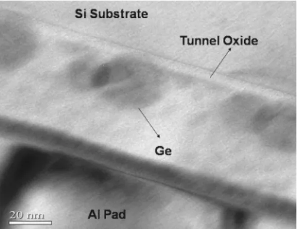
Figure 13 shows the TEM analysis of dry oxidation after 30 min plus steam treatment for 3 min. It exhibits the clearly Ge nanocrys-tal image at the interface of tunnel oxide after thermal treatment. It is considered that the memory effect as shown in Fig. 12 is contrib-uted by the Ge nanocrystals. The proposed SiGeN stack layer with high-temperature oxidized SiGeN layer, therefore, contributes both larger memory window and the additional blocking oxide deposition for the nonvolatile memory application promisingly.
The reliability characteristics, such as the retention time and en-durance, were also discussed. The charge retention time in the MOIOS structure is as shown in Fig. 14. An obvious difference of memory window can be maintained after 104s. However, the little degradation in low-VTHstate can be attributed to the effect of hole
trap states close to valence band of Ge nanocrystal.15,16In addition, the endurance characteristics for program and erase are as shown in
Fig. 15. The obvious memory window can be kept after 106
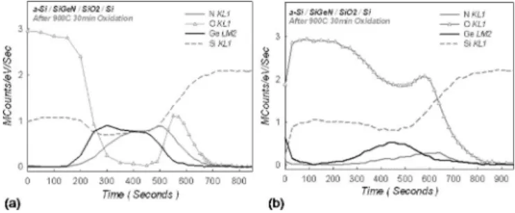
program/erase cycles. However, the threshold voltages for program and erase operation both shift to negative voltage, even if the memory window can be distinguished. It is considered that the posi-tive oxide trapped charges causes the negaposi-tive voltage shift. The AES analysis was investigated to discuss the distribution of Si, Ge, O, and N signals as shown in Fig. 16. It is found that there is a rise in oxygen signal after steam treatment. As a result, the Ge nanocrys-tals are surrounded by in SiON 共partially oxidized as SiOx兲. The Figure 10. The process flow proposed in this work with oxidized a-Si as the
blocking oxide.
Figure 11. I-V characteristics of the MOIOS structure for dry oxidation for
30 min and dry oxidation for 30 min plus steam treatment for 3 min.
Figure 12. C-V hysteresis of the MOIOS structure for the bidirectional
sweep共i兲 3 to −3 V, 共ii兲 7 to −7 V, and 共iii兲 10 to −10 V.
Figure 13. TEM analysis of the MOIOS structure with Ge nanocrystals
embedded in the dielectric layer.
program and erase curves in Fig. 7 shift to negative voltage at the same time because positive oxide trapped charges are created during the program/erase cycles in both tunnel oxide and the SiOx.17The
positive trapped charges in SiOxwill increase with the P/E cycles for the worse quality than tunnel oxide. Therefore, the threshold voltage in the Fig. 15 will shift to negative side. The obvious memory effect and good reliability can be obtained in the MOIOS structure with oxidized SiGeNas charge trapping layer.
In conclusion, the erase technology to form SiGeN stack film with both distributed storage elements and upside blocking oxide has been demonstrated successfully for nonvolatile memory appli-cation. The generation of memory windows, after a programming operation, resulted from the storage of charges in germanium nano-crystals embedded in the SiON layer. The dry oxidation causes Ge
study.
Acknowledgment
This work was performed at the National Nano Device Labora-tory and was supported by the National Science Council of the Re-public of China under contract no. NSC 95-2221-E-009-283, NSC E-009-270, NSC 95-2120-M-110-003, and NSC 95-2221-E-009-254-MY2. The authors acknowledge the support of the Plasma Enhanced Chemical Vapor Deposition system at National Chiao Tung University in Hsin-Chu. Furthermore, this work was partially supported by MOEA Technology Development for Aca-demia project no. 95-EC-17-A07-S1-046.
National Sun Yat-Sen University assisted in meeting the publication costs of this article.
References
1. D. Kahng and S. M. Sze, Bell Syst. Tech. J., 46, 1288共1967兲. 2. J. D. Blauwe, IEEE Trans. Nanotechnol., 1, 72共2002兲.
3. M. H. White, D. A. Adams, and J. Bu, IEEE Circuits Syst. Mag., 16, 22共2000兲. 4. H. E. Maes, J. Witters, and G. Groeseneken, in Proceedings of the 17th European
Solid State Devices Research Conference, p. 157共1988兲.
5. S. Tiwari, F. Rana, K. Chan, H. Hanafi, C. Wei, and D. Buchanan, Tech. Dig. - Int.
Electron Devices Meet., 1995, 521.
6. J. J. Welser, S. Tiwari, S. Rishton, K. Y. Lee, and Y. Lee, IEEE Electron Device
Lett., 18, 278共1997兲.
7. Y. C. King, T. J. King, and C. Hu, Tech. Dig. - Int. Electron Devices Meet., 1998, 115.
8. C. H. Tu, T. C. Chang, P. T. Liu, H. C Liu, C. C. Tsai, L. T. Chang, T. Y. Tseng, S. M. Sze, and C. Y. Chang, Appl. Phys. Lett., 89, 052112共2006兲.
9. F. K. LeGoues, R. Rosenberg, T. Nguyen, F. Himpsel, and B. S. Meyerson, J. Appl.
Phys., 65, 1724共1989兲.
10. J. Eugene, F. K. LeGoues, V. P. Kesan, S. S. Iyer, and F. M. d’Heurle, Appl. Phys.
Lett., 59, 78共1991兲.
11. J. Rappich, I. Sieber, and R. Knippelmeyer, Electrochem. Solid-State Lett., 4, B11 共2001兲.
12. W. K. Choi, W. K. Chim, C. L. Heng, L. W. Teo, Vincent Ho, V. Ng, D. A. Antoniadis, and E. A. Fitzgerald, Appl. Phys. Lett., 80, 2014共2002兲.
13. M. Kanoun, A. Souifi, T. Baron, and F. Mazen, Appl. Phys. Lett., 84, 5079共2004兲. 14. S. Duguay, J. J. Grob, A. Slaoui, Y. Le Gall, and M. Amann-Liess, J. Appl. Phys.,
97, 104330共2005兲.
15. V. Ioannou-Sougleridis and A. G. Nassiopoulou, J. Appl. Phys., 94, 4084共2003兲. 16. B. H. Koh, E. W. H. Kan, W. K. Chim, W. K. Choi, D. A. Antoniadis, and E. A.
Fitzgerald, J. Appl. Phys., 97, 124305共2005兲.
17. W. J. Tsai, C. C. Yeh, N. K. Zous, C. C. Liu, S. K. Cho, T. W. Samuel, C. Pan, and C. Y. Lu, IEEE Trans. Electron Devices, 51, 434共2004兲.
Figure 15. The endurance characteristics after different write/erase cycles of
Ge nanocrystals nonvolatile memory.
Figure 16. AES of MOIOS structure for共a兲 dry oxidation and 共b兲 dry