Electromigration failure mechanisms for SnAg 3.5 solder bumps on Ti Cr - Cu Cu and
Ni ( P ) Au metallization pads
T. L. Shao, Y. H. Chen, S. H. Chiu, and Chih Chen
Citation: Journal of Applied Physics 96, 4518 (2004); doi: 10.1063/1.1788837 View online: http://dx.doi.org/10.1063/1.1788837
View Table of Contents: http://scitation.aip.org/content/aip/journal/jap/96/8?ver=pdfcov Published by the AIP Publishing
Articles you may be interested in
Study of electromigration-induced Cu consumption in the flip-chip Sn Cu solder bumps J. Appl. Phys. 100, 083702 (2006); 10.1063/1.2357860
Interaction of single pentacene molecules with monatomic Cu Cu ( 111 ) quantum wires J. Vac. Sci. Technol. B 23, 1726 (2005); 10.1116/1.1942508
Increase of the thermoelectric power factor in Cu Bi Cu , Ni Bi Ni , and Cu Bi Ni composite materials J. Appl. Phys. 97, 103722 (2005); 10.1063/1.1895468
Transmission electron microscopy based study of epitaxy in Nb ( 100 ) Cu bilayer and Cu Nb ( 100 ) Cu trilayer nanoscale films
Appl. Phys. Lett. 86, 051904 (2005); 10.1063/1.1850195
Electromigration of eutectic SnPb and SnAg 3.8 Cu 0.7 flip chip solder bumps and under-bump metallization J. Appl. Phys. 90, 4502 (2001); 10.1063/1.1400096
Electromigration failure mechanisms for SnAg3.5 solder bumps
on Ti/ Cr-Cu/ Cu and Ni
„
P
…
/ Au metallization pads
T. L. Shao, Y. H. Chen, S. H. Chiu, and Chih Chena)
Department of Material Science & Engineering, National Chiao Tung University, Hsin-chu 300, Taiwan, Republic of China
(Received 19 March 2004; accepted 9 July 2004)
The electromigration behavior of SnAg3.5 solder bumps is investigated under the current densities of 1⫻104A / cm2and 5⫻103A / cm2at 150° C. Different failure modes were observed for the two stressing conditions. When stressed at 1⫻104A / cm2, damage occurred in both the anode/chip side and the cathode/chip side. However, failure happened only in the cathode/chip side under the stressing of 5⫻103A / cm2. A three-dimensional simulation of the current-density distribution was
performed to provide a better understanding of the current-crowding behavior in the solder bump. The current-crowding effect was found to account for the failure in the cathode/chip side. In addition, both the temperature increase and the thermal gradients were measured during the two stressing conditions. The measured temperature increase due to Joule heating was as high as 54.5° C, and the thermal gradient reached 365° C / cm when stressed by 1⫻104A / cm2. This induced
thermal gradient may cause atoms to migrate from the chip side to the substrate side, contributing to the failure in the anode/chip side. Moreover, the formation of intermetallic compounds in the anode/chip side may also be responsible for the failure in the anode/chip side. © 2004 American
Institute of Physics.[DOI: 10.1063/1.1788837]
I. INTRODUCTION
With the increasing environmental concerns, the micro-electronics industry is paying greater attention to lead-free solder alternatives. One of the most promising alternatives is the SnAg3.5 solder for flip-chip packages, and manufactured SnAg3.5 solder bumps on a wafer by electrical plating or printing technology is now commercially available. Further-more, the input/output pin count of flip-chip products has dramatically increased recently. In addition, bump pitch has decreased rapidly, so the contact area of the solder bumps and the diameter of the under bump metallization (UBM) continues to shrink. Therefore, electromigration of the Pb-free solder bumps has become an important issue,1,2and it needs urgently to be studied.
Previous studies on the electromigration of flip-chop sol-der bumps were mainly focused on eutectic SnPb solsol-ders.3–7 The current-crowding effect on the cathode/chip side was proposed to be responsible for the failure at the cathode/chip side of the SnPb bumps.1,6A two-dimensional simulation has been carried out to depict the current-density distribution in solder bumps. Recently, efforts have been made on the elec-tromigration of Pb-free solder bumps.8,9The current crowd-ing induced by electromigration still plays a crucial role in the failure of the bumps. In addition, thermomigration due to the thermal gradient in the flip-chip solder joints is consid-ered to account for the void formation on the anode/chip side.7 However, concerning the SnAg3.5 flip-chip solder bump on Ti/ Cr-Cu/ Cu UBM and Ni共P兲/Au pad, little re-search has been made on the failure mechanism due to elec-tromigration. We found that three failure modes occurred in
this system when the solder bumps were stressed by 5
⫻103A / cm2and by 1⫻104A / cm2. The goel of this paper is
to investigate the electromigration mechanisms of SnAg3.5 flip-chip solder bumps. In addition, since electromigration is the result of a combination of the thermal and electrical ef-fects on mass motion, a three-dimensional (3D) simulation on current-density distribution was performed to provide a better understanding of the current-crowding behavior in the solder joints. Furthermore, the temperature increase and the temperature gradients due to the current stressing in the sol-der bumps were measured to examine the thermal effect on the migration of atoms. Possible failure mechanisms respon-sible for the three failure modes are proposed.
II. EXPERIMENT
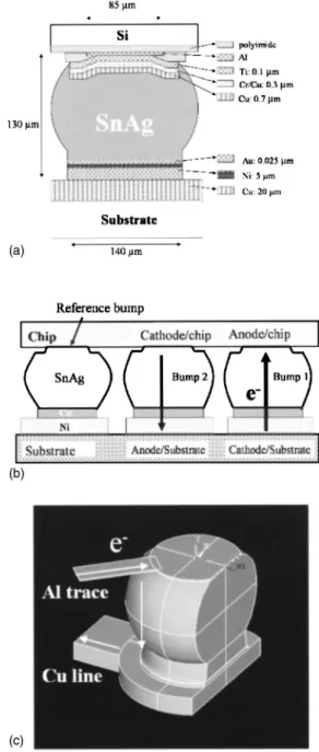
The flip-chip packages of SnAg3.5 solder bumps were prepared as follows: The chip’s size was 9.5⫻6.0 mm with a 105-m UBM diameter. The UBM consisted of 0.7m Cu, 0.3m Cr-Cu, and 0.1m Ti. A SnAg3.5 solder paste was printed and deposited on the UBM pad of the chip. The chip was reflowed in a nitrogen atmosphere oven at the 250° C peak temperature and remained above the liquid temperature for approximately 60 s. Then, the bumped die sample was prepared after sawing.
Afterward, the bumped die was mounted on a BT sub-strate, on which the SnAg3.5 solder paste was printed through a metal stencil printing on the metallization pads of the substrate. Then, the flip-chip sample was reflowed for the second time in a nitrogen atmosphere oven at the 250° C peak temperature for approximately 60 s. The flip-chip joints were formed after the second reflow. Afterward, the flip-chip package was under filled. The schematic diagram of the flip-chip sample is shown in Fig. 1(a). In this paper, we refer to
a)Author to whom correspondence should be addressed; electronic mail:
JOURNAL OF APPLIED PHYSICS VOLUME 96, NUMBER 8 15 OCTOBER 2004
0021-8979/2004/96(8)/4518/7/$22.00 4518 © 2004 American Institute of Physics
the right bump as Bump 1, in which the electron flow goes from the board side to the chip side, whereas the middle bump is Bump 2, in which the electrons migrate from the chip side to the board side. The direction of the electron flow during the current stressing is indicated by the arrows in Fig. 1(b).
To measure the temperature increase in the solder joints due to the current stressing, a solder bump was polished laterally until the contact opening was visible, with approxi-mately 97% of the mass of the bump remaining, as shown in Fig. 1(c). The current stressing of the specimen was per-formed on a hot plate in ambient air, which has a heating capacity of up to 120° C. The specimen was powered by
various currents on a hot plate maintained at 70° C. Prior to the current stressing, the emissivity of the specimen was cali-brated at 70° C. After the calibration, the bumps were pow-ered by the desired currents. Then measurement was per-formed to record the temperature distribution after the temperature reached a stable state. The temperatures in the solder joints were detected by a QFI thermal infrared micros-copy, which has a 0.1° C temperature resolution and a 2-m spatial resolution.
To prepare the plan-view specimens for observation by the scanning electron microscope(SEM), the samples were grounded either from the substrate side or the chip side until there was about 10-m-thick solder left. Then, an etching solution consisting of glycerin, nitric acid, and acetic acid at a ratio of 1:1:1 was used to selectively etch the tin. Thus, the morphology of intermetallic compound(IMC) and the whole contact opening could be observed clearly after the selective etching. Microstructure and composition were examined by a Joel 6500 field-emission SEM and energy dispersive spec-troscopy(EDS), respectively.
III. RESULTS
Figure 2(a) shows the cross-sectional SEM image of a solder bump without thermal annealing and current stressing. IMCs of 共Cu,Ni兲6Sn5 were found on the interface of the
solder and the metallization layer in the substrate side. How-ever, there were no obvious IMCs observed in the vicinity of the UBM on the chip side. Figure 2(b) depicts the bump microstructure after thermal annealing at 150° C for 20 h. IMCs of 共Ni,Cu兲3Sn4 formed at the interface of the solder FIG. 1. Schematic diagrams of the bumps used in this study: (a)
Cross-sectional view showing the structure of a SnAg bump.(b) Schematic
dia-gram of the bumps during current stressing. The directions of the electron flow are indicated by arrows in the figure. (c) Schematic diagram of the bump for temperature and thermal gradient measurement, in which 97% of the solder remains. An infrared microscope was used to measure the tem-perature increase and the thermal gradient on the polished surface.
FIG. 2. (a) Cross-sectional SEM image of an as-prepared SnAg solder bump.(b) Cross-sectional SEM image of a SnAg bump aged at 150°C for
20 h.
J. Appl. Phys., Vol. 96, No. 8, 15 October 2004 Shaoet al. 4519
and the Ni pad in the substrate side after the solid-state ag-ing. Furthermore, several large Ag3Sn particles were
ob-served in the bulk solder, as seen in Fig. 2(b). A slight amount of 共Cu,Ni兲6Sn5 IMC in the solder bump near the
substrate side was occasionally observed. Again, no large amount of Cu-Ni-Sn IMC was seen in the chip side.
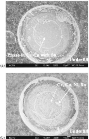
To examine the microstructure evolution on the contact opening of the chip side after the current stressing, the SnAg solder was etched selectively to allow a plan-view observa-tion of the contact, which can provide more informaobserva-tion on the failure mechanism when the electromigration damage oc-curs in the UBM. In addition, the IMC formation on the contact opening can be clearly observed because the etchant does not etch the Cu-Ni-Sn IMCs and the UBM. Figure 3(a) depicts the plan-view SEM image of the contact opening on the chip side when the SnAg solder was etched away, and the whole contact opening can be clearly seen. The inner circle is the contact opening for the solder bump connecting to the Al trace on the chip side. No obvious IMCs were found to attach to the UBM. Figure 3(b) shows the plan view of the chip side that was only thermally annealed at 150° C for 20 h. Several IMCs were observed after the thermal anneal-ing, as indicated by the arrow in Fig. 3(b). The EDS results indicated that they consisted of Sn, Ni, Cu, and Cr. The Ni atoms may migrate from the substrate side during the anneal-ing process.
Surprisingly, both the anode/chip and the cathode/chip sides of the SnAg bumps may be damaged after the current
stressing by 1⫻104A / cm2at 150° C. However, the damage
may occur on both sides or only on one of them. The current density was calculated based on the area of contact opening on the chip side. In these packages, the contact opening was 85m in diameter on the chip side, whereas it was 150m in diameter for the pad opening on the substrate side. Thus, the current density on the chip side was about three times larger than that of the substrate side. Therefore, electromi-gration damage generally occurs on the chip side. Figure 4 shows the cross-sectional SEM images of the bump pairs after the current stressing by 1⫻104A / cm2 at 150° C for 22 h. Open failure occurred after the current stressing, and voids formed near the chip sides of the bump pairs. On the anode/chip side, as shown in Fig. 4(a), voids/cracks can be observed near the UBM. In addition, IMCs of 共Ni,Cu兲3Sn4 can be detected below the UBM, as indicated by one of the arrows in the figure. On the cathode/substrate side, the IMCs also grew larger. Some IMCs inside the solder were deter-mined to be 共Cu,Ni兲6Sn5. On the cathode/chip side, as shown in Fig. 4(b), voids are also found inside the solder below the UBM. Furthermore, the voids on the right side are bigger than those on the left side. The IMCs on the anode/ substrate side grew bigger. Elemental EDS mapping of Ti, Cr, Cu, and Ni were performed for the bump pairs, as shown in Fig. 5. The UBM layers for both bumps were damaged, and Ni and Cu atoms were detected accumulating in the sol-der near the center of the UBM on the anode/chip side. The Ni atoms had migrated from the substrate to the chip side in the same direction as the electron flow. Since the thermal gradient in the bump drove the atoms from the chip side to the substrate side,7 the electrical field could be the major
FIG. 3. Plan-view SEM images showing the morphology of the contact openings on the chip side for(a) an as-prepared SnAg solder bump and (b) a SnAg bump aged at 150° C for 20 h. Ternary compound of Ni, Cu, and Sn were found after the aging.
FIG. 4. Cross-sectional SEM image after the current stressing of 1
⫻104A / cm2at 150° C for 22 h(a) for Bump 2 and (b) for Bump 1. Voids formed on both the cathode/chip and anode/chip sides.
4520 J. Appl. Phys., Vol. 96, No. 8, 15 October 2004 Shaoet al.
driving force causing Ni atoms to migrate from the substrate side to the chip side. However, the Cu atoms may have come from the UBM either on the chip side or from the substrate side, since part of the Ni layer in the substrate side was damaged.
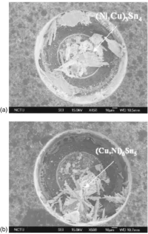
Plan views for the contact opening on the chip side were prepared to investigate the failure mechanism. Figure 6 shows the microstructures of the contact openings of another bump pair that failed after the current stressing of 1
⫻104A / cm2 at 150° C for 22 h. Both contact openings for
the anode/chip and the cathode/chip sides were clearly shown after the selective etching of Sn. On the anode/chip side, as seen in Fig. 6(a), many IMCs formed at the contact opening and their composition is close to共Ni,Cu兲3Sn4. How-ever, on the cathode/chip side, dendritelike IMCs can be ob-served, with the composition close to 共Cu,Ni兲6Sn5.
Com-pared with the reference bumps, it is concluded that the formation of共Ni,Cu兲3Sn4and共Cu,Ni兲6Sn5 was mainly due
to the current stressing because few IMCs formed in the reference bump. The morphology of dendritelike IMCs indi-cates that both 共Ni,Cu兲3Sn4 and 共Cu,Ni兲6Sn5 have highly
anisotropic surface energy and that the solder may have melted. We shall discuss this point in Sec. IV.
To investigate the failure mechanism at a lower current density, another set of bump pairs was stressed by 5
⫻103A / cm2 at 150° C. In this set, failure occurred only in
the cathode/chip end of the bump, whereas no noticeable damage was observed for the anode/chip side. Figure 7(a) shows the cross-sectional SEM image on the failure site after a 192-h current stressing. The UBM collapsed, and some of the SnAg solder filled in where the UBM had been located. The EDS analysis is shown in Fig. 7(b), indicating that the Al pad and the UBM were embedded into the solder. The IMCs of CuAl2formed at the location where the Al pad had
situated, as indicated in the figure. The plan views for an-other set of failed bump pairs are seen in Fig. 8. On the contact opening of the anode/chip side, no obvious damage was observed except for the mixing of Al and Cr atoms in the lower part of the opening, as seen in Fig. 8(a).
Neverthe-FIG. 5. Elemental EDS mappings of Ti, Cr, Cu, and Ni for the bump pairs in Fig. 5. Ni and Cu atoms accumulated on the anode/chip side.
FIG. 6. Plan-view SEM images depicting the morphology of the contact openings after the stressing of 1⫻104A / cm2at 150° C for 22 h(a) on the anode/chip and(b) on the cathode/chip side. IMCs formed on both sides.
FIG. 7. Cross-sectional SEM images for the bumps after current stressing of 5⫻103A / cm2 at 150° C for 218 h (a) for bump 2, in which electrons drifted downward and(b) for the enlarged image on the cathode/chip side.
J. Appl. Phys., Vol. 96, No. 8, 15 October 2004 Shaoet al. 4521
less, the contact opening on the cathode/chip side was de-stroyed completely, and the rough interface consisted of Al, Sn, Cr, and Ti, as shown in Fig. 8(b).
To examine the Joule heating effect on the failure mechanism, both the temperature increase and the thermal gradient were measured for the two stressing conditions. Fig-ure 9(a) and 9(b) show the temperature increase and the ther-mal gradient, respectively, when the package was stressed at 1⫻104A / cm2共0.59 A兲. The measured temperature increase in the solder was as high as 54.5° C. In addition, the tem-perature increase due to Joule heating slightly depended on the testing temperature. It decreased approximately by 5 ° C when the testing temperature increased from 70 to 100° C. Therefore, although the testing temperature was maintained at 150° C, the real temperature inside the solder might be over 200° C. The thermal gradient under the stressing condi-tion was measured to be 369° C / cm. In contrast, when the package was stressed at 5⫻103A / cm2, the average
tem-perature increase was detected to be 9.1° C and its thermal gradient became 127° C / cm.
IV. DISCUSSION A. Failure mechanisms
Multiple driving forces may trigger the migration of at-oms in the SnAg bumps during current stressing. According to the electromigration theory,10,11voids form at the cathode and extrusions or hillocks accumulate at the anode. Thus, open failure occurs at the cathode side. However, in SnAg
bumps, open failure happend not only in the cathode end but also in the anode side, which implies that other failure mechanisms may take place during the current stressing. During the current stressing of flip-chip solder bumps, the following two driving forces may operate due to their unique geometry and composition and thus, influence their elec-tromigration behavior.
1. Electrical effect of current crowdling on electromigration
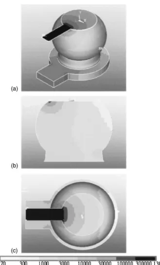
Current-crowding plays a critical role in the electromi-gration failure of the solder bump, because the current den-sity in the Al trace is typically one or two orders in magni-tude larger than that in the solder.1,6Current crowding occurs in the junction of the Al trace and the solder bump. However, current-density distribution in the flip-chip bumps is a three-dimensional issue. Figure 10 depicts the current-density dis-tribution by simulation of the solder joint. The 3D tilt view of the current-density distribution is shown in Fig. 10(a), in which a 0.59 A was applied. The corresponding current den-sity in the Al trace is 9.8⫻105A / cm2, and the calculated average current density in the contact opening of the chip side is 1.0⫻10 A/cm2. However, current crowding occurs at the entrance point of the Al trace into the solder bump. The maximum current density inside the solder is as high as 1.8⫻105A / cm2, as seen in the cross-sectional view along
the Z axis in Fig. 10(b). On the substrate side, the current-crowding phenomenon is much less due to the larger contact opening. Figure 10(c) illustrates the current-density distribu-tion on the contact opening in the chip side. The red area close to the entrance into the solder bump represents the region with a high current density and the most vulnerable area in the joint during electromigration testing.
Void formation caused by current crowding can be ob-served in Fig. 4(a), in which the electron flow entered the bump from the right-back side. Significant flux divergence
FIG. 8. Plan-view SEM images showing the morphology of the contact opening after stressing by 5⫻103A / cm2 at 150° C for 218 h (a) on the anode/chip side and(b) on the cathode/chip side. Failure occurred at the cathode/chip side.
FIG. 9. (a) Temperature distribution in the SnAg bump when stressed at 1 ⫻104A / cm2 at 70° C. The temperature increase due to the current was 54.5° C(b) The corresponding temperature profile along the dashed line in
(a), showing a thermal gradient of 365°C cmacross the bump.
4522 J. Appl. Phys., Vol. 96, No. 8, 15 October 2004 Shaoet al.
occurred in this area, causing a void formation in the vicinity of the entrance point. In addition, the IMC formation in Fig. 6(b) also demonstrates the current-crowding effect on elec-tromigration. The electrons entered the bump from the loca-tion of the root of the IMCs situated on the chip side, going vertically to the paper plane toward the substrate, and then flowed downward to the Cu line. Thus, the growth direction of the IMCs matches the current-crowding path. This path can be seen in Fig. 10(b) and indicates that it is from the top-left corner downward to the bottom-left corner. Thus, current crowding plays a key role in the damage formation in the cathode/chip end.
2. Thermal effect of Joule beating on electromigration
During the current stressing in flip-chip package, Joule heating may cause a temperature increase and result in a thermal gradient. The former raises the testing temperature higher than the ambient temperature, resulting in a higher diffusion rate for the materials in the bumps. The latter pro-duces another driving force for atomic migration, which may
trigger a failure mechanism other than the current-crowding-induced failure. As shown in Fig. 9(a), the temperature in-crease when stressed at 1⫻104A / cm2 was as high as
54.5° C, which means that the real testing temperature may be over 200° C. Thus, formation of many IMCs during the current stressing occurred on the anode/chip side, as shown in Fig. 6(b). Furthermore, prior to the failure, the temperature in the bump may exceed its melting point, causing local melting or the melting of the whole bump. It is reported that the SnAgCu solder bumps may have melted upon failure when they were stressed with a current density of 2
⫻104A / cm2 at 100° C.12
Thus, it is hypothesized that the dendritic IMCs in Fig. 6(b) might be formed in the liquid state, since dendrite growth occurs only in the liquid state.13 Hence, it is worthy to note that the testing condition of 150° C and 1⫻104A / cm2 may be too stringent for the SnAg solder, which has a melting point of 221° C.
In addition, this temperature increase will affect the mea-surement of the mean-time-to-failure(MTTF), which is typi-cally expressed as14
MTTF = A1
jnexp
冉
Q kT
冊
,where A is constant, j is the current density, n is a model parameter for current density, Q is the activation energy, k is the Bolzmann’s constant, and T is the average bump tem-perature. The real temperature in the solder during high-current stressing is much higher than the testing temperature. So the measured value of MTTF could be underestimated.
The thermal gradient drives the atoms from the chip side to the substrate side, leaving voids near the UBM on the chip side. Since the temperature in the solder near the chip side is higher than that in the substrate side, the jumping frequency of the solder in the chip side is higher, causing a net atomic flux from the chip to the substrate side.15 Hopkins et al. reported that thermal migration may assist electromigration in the cathode/chip side and may oppose electromigration in the anode/chip side.7 The measured thermal gradient was 369° C / cm when stressed at 1⫻104A / cm2, which may
con-tribute to the formation of voids in the anode/chip side, as seen in Fig. 4(b). On the other hand, when the bumps were stressed by 5⫻103A / cm2 at 150° C, failure occurred only
in the cathode/chip side. The average temperature increase was detected to be 9.1° C at the current density, and its ther-mal gradient decreased to 127° C / cm, as seen in Fig. 9. Therefore, both the temperature increase and the thermal gra-dient effects became less profound and thus, current crowd-ing dominated the failure mechanism at the lower current density.
V. CONCLUSIONS
Electromigration-induced failure in SnAg3.5 solder bumps has been investigated under the current densities of 1⫻104 A / cm2and 5⫻103A / cm2at 150° C. When stressed
at 1⫻104A / cm2, failure may occur on both the anode/chip
and the cathode/chip sides. Joule heating became very seri-ous under the 1⫻104A / cm2 current stressing, causing a
temperature increase of 54.5° C in the solder and a thermal
FIG. 10. Three-dimensional simulation of current-density distribution in a SnAg bump when powered by 0.59 A.(a) Tilt view of the current-density
distribution for the whole joint. Current densities in the Al trace, solder bump, and Cu line are labeled in the figure.(b) Current-density distribution in the cross section along the dashed line in(a). (c) Top view showing the current-density distribution in the contact opening on the chip side. Current crowding occurs in the vicinity of the junction of the Al trace and the solder bump.
J. Appl. Phys., Vol. 96, No. 8, 15 October 2004 Shaoet al. 4523
gradient of 365° C / cm across the solder bump. Thermal mi-gration due to the built thermal gradient and volume expan-sion due to the IMCs formation may account for the void formation on the anode/chip side under the stressing of 1
⫻104A / cm2. Three-dimensional simulation on
density distribution supported the contention that current-crowding effect was considered to be responsible for the fail-ure on the cathode/chip side. This is because for the solder bumps stressed under 5⫻103A / cm2, migration of Al atoms
in the Al trace may contribute to the UBM failure in the cathode/chip side.
ACKNOWLEDGMENTS
The authors would like to thank Professor D.J. Yao in National Tsing Hua University for the temperature measure-ment and Professor K. N. Tu at UCLA for the helpful dis-cussions, and the National Science Council of R. O. C. for the financial support of this study through Grant No. 90-2216-E-009-042. In addition, the simulation assistance from the National Center for High-Performance Computing
(NCHC) in Taiwan is appreciated.
1
K. N. Tu, J. Appl. Phys. 94, 5451(2003).
2
K. N. Tu and K. Zeng, Mater. Sci. Eng., R. R34, 1(2001).
3
S. Brandenburg and S. Yeh, Proceedings of Surface Mount International
Conference and Exhibition, SM198, San Jose, CA, 23-27 August 1998
(San Diego, CA, 1998), pp. 337–344.
4
C. Y. Liu, C. Chen, C. N. Liao, and K. N. Tu, Appl. Phys. Lett. 75, 58
(1999).
5
J. D. Wu, P. H. Zheng, K. Lee, C. T. Chiu, and J. J. Lee, Proceedings of
the 52nd Electronic Components and Technology Conference, ECTC 2002, San Diego, CA, 28 May 2002(San Diego, CA, 2002) pp. 452–457.
6
E. C. C. Yeh, W. J. Choi, K. N. Tu, P. Elenius, and H. Balkan, Appl. Phys. Lett. 80, 580(2002).
7
H. Ye, C. Basaran, and D. Hopkins, Appl. Phys. Lett. 82, 7(2003).
8
T. Y. Lee, D. T. Frear, and K. N. Tu, J. Appl. Phys. 90, 4502(2001). 9
S. Y. Jang, J. Wolf, W. S. Kwon, and K. W. Paik, Proceedings of the 52nd
Electronic Component and Technology Conference, ECTC 2002, San Di-ego, CA, 28 May 2002(San Diego, CA, 2002) pp. 1213–1220.
10
I. A. Blech, J. Appl. Phys. 47, 1203(1976).
11
R. Landauer and J. W. F. Woo, Phys. Rev. B 10, 1266(1974). 12
Y. C. Hsu, T. L. Shao, C. J. Yang, and C. Chen, J. Electron. Mater. 32(11), 1222(2003).
13
D. A. Porter and K. E. Easterling, Phase Transformations in Metals and
Alloys, 2nd ed.(Chapman & Hall, London, 1992), p. 220.
14
J. R. Black, IEEE Trans. Electron Devices ED-16(4), 338 (1969).
15
P. Shewmon, Diffusion in Solids, 2nd ed.(The Minerals, Metals & Mate-rial Sociey, Warrendale, PA, 1989), Chap. 5.
4524 J. Appl. Phys., Vol. 96, No. 8, 15 October 2004 Shaoet al.