IEEE ELECTRON DEVICE LETTERS, VOL. 22, NO. 4, APRIL 2001 179
Schottky Barrier Thin-Film Transistor (SBTFT) with
Silicided Source/Drain and Field-Induced Drain
Extension
H. C. Lin, Member, IEEE, K. L. Yeh, R. G. Huang, C. Y. Lin, and T. Y. Huang, Member, IEEE
Abstract—A novel Schottky barrier thin-film transistor
(SBTFT) with silicided source/drain and field-induced drain (FID) extension is proposed and demonstrated. In the new device configuration, a metal field-plate (or sub-gate) lying on the passivation oxide is employed to induce a sheet of carriers in a channel offset region located between the silicided drain and the active channel region underneath the main-gate. The new device thus allows ambipolar device operation by simply switching the polarity of the bias applied to the field plate. In contrast to the conventional SBTFT that suffers from high GIDL (gate-induced drain leakage)-like off-state leakage current, the new SBTFT with FID is essentially free from the GIDL-like leakage current. In addition, unlike the conventional SBTFT that suffers from the low on–off current ratio, the new device exhibits high on/off current ratio up to106 for both n- and p-channel modes of operation. Moreover, the implantless feature and the ambipolar capability of the new device also result in extra low mask count for CMOS processes integration. These excellent device characteristics, coupled with its simple processing, make the new device very promising for future large-area electronic applications.
Index Terms—Ambipolar, field-induced drain, Schottky barrier,
thin-film transistor.
T
HE SCHOTTKY barrier (SB) MOS transistor, which utilizes metallic source and drain, was first demonstrated 30 years ago [1]. As compared with the conventional MOSFET, it possesses several advantages including simpler fabrication, elimination of the implant step for forming source/drain, and better short-channel effect control [2], [3]. In addition, it has the capability of bichannel operation [4]. However, it suffers from severe leakage current and poor on/off current ratio [4]–[6], due to the much larger junction leakage current inherent in a Schottky diode. To make things worse, it is almost impossible to fabricate SB MOS transistors with acceptable n- and p-channel characteristics simultaneously for ambipolar operation [4], owing to the constraint imposed by the fixed barrier height of the Schottky contact.To this date, SB MOS transistors reported in the literature were fabricated on either bulk or silicon-on-insulator (SOI)
sub-Manuscript received November 22, 2000. This work was supported by the National Science Council of Taiwan under Contract NSC-89-2215-E-317-015. The review of this letter was arranged by Editor T.-J. King.
H. C. Lin and C. Y. Lin are with the National Nano Device Laboratories, Hsinchu 300, Taiwan, R.O.C. (e-mail: [email protected]).
K. L. Yeh and R. G. Huang are with the Institute of Electronics, National Chiao Tung University, Hsinchu 300, Taiwan, R.O.C.
T. Y. Huang is with the National Nano Device Laboratories, Hsinchu 300, Taiwan, R.O.C., and the Institute of Electronics, National Chiao Tung Univer-sity, Hsinchu 300, Taiwan, R.O.C.
Publisher Item Identifier S 0741-3106(01)02857-9.
strate [1]–[6]. These devices thus have a mono-crystalline Si ac-tive channel region. To the best of our knowledge, no work on SB poly-Si thin-film transistors (TFTs) has ever been reported. One plausible explanation is that the existence of grain bound-aries in the channel may further degrade the junction character-istics, thus renders the resultant device totally unacceptable and useless.
In this work, we proposed and demonstrated, for the first time, a novel poly-Si TFT device that can effectively alleviate the aforementioned shortcomings [7]. The new device features a field-plate (or subgate) that can induce an electrical drain ex-tension in the active poly-Si layer. This unique design not only effectively increases the on/off current ratio, but also enables ac-ceptable ambipolar operation on the same device.
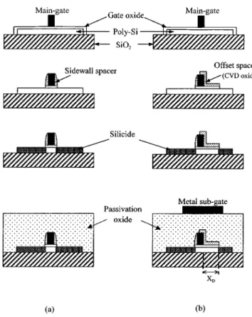
Fig. 1(a) and (b) show the key fabrication steps for devices with the conventional and the proposed structure with FID, re-spectively. Here, the “conventional” devices refer to those fabri-cated by using the sidewall spacer to isolate the gate and S/D re-gions during subsequent self-aligned silicidation (salicidation) step. Such scheme is commonly adopted for conventional SB MOSFET fabrication [1]–[6]. Briefly, the fabrication begins by depositing an amorphous Si layer (50 nm) at 550 C using low-pressure chemical vapor deposition (LPCVD) on 6 in. Si wafers capped with a thermal oxide layer. The amorphous Si layer was subsequently transformed into polycrystalline phase by a solid-phase recrystallization (SPC) treatment at 600 C in N for 24 h to serve as the active device layer. After patterning the active region, a 20 nm CVD gate oxide and a n poly-Si (200 nm) layer was deposited. The n poly-Si layer was then patterned to form the main-gate. Next, a CVD oxide layer (200 nm) was deposited and a photolithographic step was used to define the offset regions for the proposed TFT device [Fig. 1(b)]. During the reactive-ion-etching step, a self-aligned sidewall spacer was simultaneously formed for the conventional devices [Fig. 1(a)]. Afterwards, a self-aligned silicidation (salicidation) treatment was performed to form the silicided source/drain. This was ac-complished by depositing a thin Co layer (15 nm, capped with 30 nm of TiN) on the wafer, followed by a rapid-thermal an-nealing (550 C, 30 s) step. A wet etching step in a solution (H SO : H O ) was then used to remove the nonre-acted metals. It should be noted that neither the channel nor the source/drain received any deliberate doping, therefore no post-implant annealing step was necessary. Wafers then followed a standard back-end processing to form contact pads, and received a plasma treatment at 250 C in NH for 1 hour before mea-surements. It is worthy to note here that the metal subgate was
180 IEEE ELECTRON DEVICE LETTERS, VOL. 22, NO. 4, APRIL 2001
Fig. 1. Key fabrication flows for SBTFT devices with (a) conventional and (b) the proposed structure with field-induced drain (FID).X in (b) is the length of FID region in the channel.
formed during the regular metal patterning, so no extra steps were required.
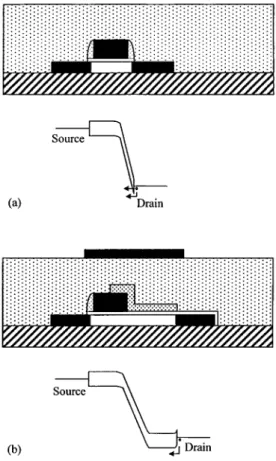
The new structure [Fig. 1(b)] features an undoped Si active channel, a top metal field-plate (i.e., the subgate), and Schottky source/drain. During device operation, a high fixed voltage is applied to the subgate to form a field-induced drain extension under the subgate region. So depending on the polarity of the subgate bias, the device can be set for n-channel operation with positive sub-gate bias, or p-channel operation with negative sub-gate bias. The new device is similar to conventional SB MOSFET devices [1]–[6], with the exception of a field-induced drain extension located between the channel and the Schottky drain. The existence of the field-induced drain extension mainly serves to reduce the substantial off-state leakage that have plagued all previous SB MOSFETs. The new device is also similar to MOSFET’s with field-induced drain (FID) [8], [9], except that the heavily-doped source/drain region is replaced by Schottky source/drain. While retaining all the advantages of FID such as low off-state leakage and low junction leakage, the use of Schottky source/drain not only reduces processing steps (i.e., implant and subsequent annealing), but also allows ambipolar operation, thus greatly simplify processing steps especially for CMOS process integration.
Figs. 2 and 3 show the ambipolar (i.e., both n- and p-channel) subthreshold characteristics of conventional and FID SBTFT, respectively. SBTFT with conventional structure exhibits very poor performance for both p- and n-channel modes of operation. On/off current ratios are around or less than . Moreover, the strong GIDL (gate-induced drain leakage)-like leakage current
Fig. 2. Typical ambipolar (i.e., p- and n-channel) subthreshold characteristics of SBTFT with conventional structure.
Fig. 3. Typical ambipolar subthreshold characteristics of SBTFT with FID.
results in the V-shaped current–voltage curves. In contrast, su-perior p- and n-channel device performances are simultaneously realized on the SBTFT with FID structure when a proper bias is applied to the subgate. As shown in Fig. 3, on/off current ratio as high as are observed for both n- and p-channel modes of operation. It should be emphasized that the characteristics are obtained on the same device by simply changing the polarity of the subgate bias. By comparing Figs. 2 and 3 in detail, it can be seen that not only the on-state current is improved with the new structure, but the GILD-like leakage current is also effectively eliminated, further highlighting the effectiveness of FID.
LIN et al.: SBTFT WITH SILICIDED SOURCE/DRAIN 181
Fig. 4. Band diagrams for n-channel operation of SBTFT’s with conventional structure (a) and FID (b) at off-state. (i.e.,V = 0, V = V , and
V 0).
The improvement on the on-state current could be ascribed to the elimination of the ungated channel regions existing under the sidewall spacers in the conventional device. Since the bottom width of the sidewall spacers ( nm) is longer than the silicide thickness ( nm), the silicided source/drain portion would not reach the channel region beneath the main-gate, leading to an increase in the parasitic resistance along the channel in the conventional device. This feature is quite different from that of SB MOS devices reported previously [4]–[6] in which the silicide source/drain overlap with the gate. Although a self-aligned sidewall spacer also exists at the source side of our new device, however, the overlying metal subgate effectively covers the channel region underneath the spacer and could thus reduce the parasitic resistance when a high subgate bias is applied.
Detailed analysis on the conduction mechanisms of the leakage current is still in progress. One possible qualitative explanation for the reduction of the off-state current with FID is given in Fig. 4. For the conventional device, a high electric field develops in the channel near the drain side [Fig. 4(a)]. Such a high field would enhance the field emission as well as thermionic emission of holes from the silicided drain. On the other hand, formation of the FID with the band diagram shown in Fig. 4(b) tends to suppress the emission of holes from the drain. As a result, GIDL-like leakage could be eliminated.
The proposed device structure and its fabrication process are advantageous in many respects. Firstly, the channel and source/drain doping and subsequent annealing steps are eliminated altogether, making the overall process flow much
simplified and very suitable for low-temperature manufac-turing. Secondly, the new structure is actually compatible with metal-gate processing, making feasible for the first time a fully implantless CMOS process (by using metal such as TiN as the main-gate material). Third, since the silicidation step for forming Schottky source/drain is self-aligned and the metal subgate could be formed during the metal interconnect step, no additional masking and processing steps are needed. Fourth, the fully implantless process combined with the ambipolar nature greatly simply CMOS process integration, making possible an extra low mask-count CMOS process that is not feasible previously. Finally, the unique device structure makes feasible for the first time ambipolar mode with superior characteristics, as is demonstrated in this work. The low current required for the subgate bias also allows the use of on-chip bias generator to simplify outside voltage supply.
In summary, a novel implantless Schottky barrier thin-film transistor (SBTFT) with silicided source/drain and field-in-duced drain (FID) extension capable of ambipolar operation is proposed and successfully demonstrated. While the conven-tional SBTFT depicts large GIDL-like leakage current and low on/off current ratio of less than , the new device depicts GIDL-free characteristics with on/off current ratio as high as for both n- and p-channel modes of operation on the same device. The superior characteristics, together with its simple processing, low thermal budget, and low mask-count in CMOS integration, make the new device very promising for future large-area electronic applications.
ACKNOWLEDGMENT
The authors would like to thank Prof. S. M. Sze for his en-couragement and support during the course, and their colleagues at the National Nano Device Laboratories for their assistance in device fabrication. The authors are also grateful to the anony-mous reviewers for their valuable comments and suggestions.
REFERENCES
[1] T. Lepselter and S. M. Sze, “SB-IGFET: An insulated-gate field-effect transistor using Schottky barrier contacts for source and drain,” Proc. IEEE, pp. 1400–1401, 1968.
[2] J. R. Tucker, C. Wang, and P. A. Carney, “Silicon field-effect transistor based on quantum tunneling,” Appl. Phys. Lett., vol. 65, pp. 618–620, 1994.
[3] W. Saitoh, A. Itoh, S. Yamagami, and M. Asada, “Analysis of short-channel Schottky source/drain metal-oxide-semiconductor field-effect transistor on SOI substrate and demonstration of sub-50 nm n-type de-vice with metal gate,” Jpn. J. Appl. Phys., vol. 38, pp. 6226–6231, 1999. [4] M. Nishisaka, Y. Ochiai, and T. Asano, “Pt-Si source and drain SOI-MOSFET operating in bi-channel mode,” in Proc. Device Res. Conf. (DRC), 1998, pp. 74–75.
[5] C. Wang, J. P. Snyder, and J. R. Tucker, “Sub-40 nm PtSi Schottky source/drain metal-oxide-semiconductor field-effect transistor,” Appl. Phys. Lett., vol. 74, pp. 1174–1176, 1999.
[6] A. Itoh, M. Saitoh, and M. Asada, “A 25-nm-long channel metal-gate p-type Schottky source/drain MOSFET on SOI substrate,” Jpn. J. Appl. Phys. (Part I), vol. 39, pp. 4757–4578, 2000.
[7] H. C. Lin et al., “A novel implantless MOS thin-film transistor with simple processing, excellent performance and ambipolar operation ca-pability,” in IEDM Tech. Dig., 2000, pp. 857–859.
[8] T. Y. Huang et al., “A simpler 100-V polysilicon TFT with improved turn-on characteristics,” IEEE Electron Device Lett., vol. 11, pp. 244–246, 1990.
[9] , “Device sensitivity of field-plated polysilicon high-voltage TFT’s and their application to low-voltage operation,” IEEE Electron Device Lett., vol. 11, pp. 541–543, 1990.