www.elsevier.nl / locate / mee
RIE lag in diffractive optical element etching
a ,
*
b a,cJyh-Hua Ting
, Jung-Chieh Su , Shyang Su
a
National Nano Device Laboratories, 1001-1 Ta Hsueh Road, Hsinchu 30050, Taiwan
b
Opto-Electronics& Systems Laboratories, Industrial Technology Research Institute, Bldg. 44, Q300 195,
Chung Hsing Road, Section 4, Chutung, Hsinchu 31015, Taiwan
c
Department of Electronic Engineering, National Chiao-Tung University, 1001 Ta Hsueh Road, Hsinchu 30050, Taiwan
Received 13 August 1999; accepted 17 October 1999
Abstract
In this study, the pattern of a 4 mm diameter diffractive optical element with linewidth ranging from 12 to 0.5 mm was adopted. With the SiO layer as the etch hard mask, silicon was etched based on HBr chemistry with additions of O and2 2
SF . The effects of O content on the sidewall anisotropy, etch rate, and etch selectivity over the SiO mask were also6 2 2 examined. The RIE lag, where etching of a small trench (hole) lags behind a large trench (hole), was investigated to produce an optimum aspect ratio for each zone of the diffractive optical element. The regression relation of the etch depth versus zone width was determined as a guideline for the feasibility of this method. 2000 Elsevier Science B.V. All rights reserved.
Keywords: RIE lag; Diffractive optical elements; Anisotropic etching
1. Introduction
A diffractive optical element, e.g., diffractive microlens, is composed of zone structure by removing the multiple modulo 2p phase from the refractive lens technique. The diffraction efficiency is determined by the surface profile within a specified zone. However, the surface profile of this relief structure relies on the fabrication techniques, such as lithography, ion etching, etc. Due to the limitation of process equipment the diffraction efficiency of a binary surface profile is usually lower than the expected value. Specifically, the aspect ratio of each zone pitch is one of the main parameters determining the diffraction efficiency. How to control the aspect ratio under the limitation of various etching conditions is becoming a pursuing topic for most of the related research. In this paper, reactive ion etching (RIE) lag was used to obtain the existing optimum aspect ratio for each zone, i.e., the aspect ratio should be consistent throughout all zones. In other words, RIE lag may produce an
*Corresponding author.
E-mail address: [email protected] (J.-H. Ting).
0167-9317 / 00 / $ – see front matter 2000 Elsevier Science B.V. All rights reserved. P I I : S 0 1 6 7 - 9 3 1 7 ( 9 9 ) 0 0 4 5 0 - 5
optimum aspect ratio for each zone, then the diffraction efficiency of the diffractive lens can be optimized. Therefore, RIE lag where etching of a small trench (hole) lags behind a large trench (hole) [1,2] was investigated in this work. The regression relation of the etch depth versus zone width was determined as a guideline for the feasibility of this method. In this study, the pattern of a 4 mm diameter diffractive optical element with linewidth ranging from 12 to 0.5 mm was adopted. The silicon etching was based on HBr chemistry.
2. Experimental
The experiments were performed in an electron cyclotron resonance (ECR) reactor on 150-mm diameter wafers. To etch silicon deeply, a 1.2-mm thick silicon dioxide layer was deposited via thermally wet oxidation as the etch hard mask. After the lithographic process, the oxide layer was etched with a CF / CHF /Ar mixture in a RIE process. Then, the photoresist was stripped.4 3 Afterwards, the pattern was transferred to the silicon substrate by the etch process based on HBr chemistry with additions of O and SF . Finally, a 6:1 (NH F:HF)-buffered hydrofluoric acid dip was2 6 4 carried out to remove the remaining SiO layer and the sidewall passivation film and the process was2 completed.
Feature width and etch depth measurements were made by scanning electron microscopy (SEM). SEM was also exploited to evaluate the sidewall anisotropy and the quality of the etched surface. The SiO etch rate was determined from the thickness variation before and after silicon etching. Quoted2 etch rates were an average of several points across a wafer. The effects of O content on the sidewall2 anisotropy, etch rate, and etch selectivity over the SiO mask were explored. With appropriate O2 2 concentration, SF was added to achieve vertical sidewall and smooth surface.6
A diffractive optical element, e.g., diffractive microlens, is composed of a zone structure, according to a standard modulo 2p phase technique to produce the zone structure. For example, the zone radius
rm of a zone plate is given by 1 / 2
r 5 (2mm lf ) (1)
where m is the zone index number, l is the illumination wavelength, and f is the focal length. The phase profile is approximated by a discrete stepped profile with rm getting narrower when close to the edge of diffractive microlenses. The diffraction efficiency of such a lens is strongly dependent on the profile of each zone pitch [3,4]. Specifically, the aspect ratio of each zone pitch, i.e., the ratio of depth / line width [5]. In other words, there is existing an optimum aspect ratio for each zone, i.e., the aspect ratio should be consistent throughout all zones. In our system, the aspect ratio of each zone of the diffractive lens is changing for fixed etch depth; therefore, the diffraction efficiency cannot be optimized if no RIE lag occurs. On the other hand, RIE lag may produce an optimum aspect ratio for each zone, then the diffraction efficiency of diffractive lens can be optimized. However, in this approach, various etch depths are required with the largest depth in the center and decreasing toward the boundary. Specifically, this leads to a lessening of the disadvantages of binary optics [6,7] for low diffraction efficiency. Therefore, RIE lag where high aspect ratio features have reduced etch rates [1,2] was investigated in this work. The regression relation of the etch depth versus zone width was determined as a guideline for the feasibility of this method. In this study, the pattern of a 4-mm diameter diffractive optical element with linewidth ranging from 12 to 0.5 mm was adopted.
3. Results and discussion
With the SiO layer as the etch hard mask, silicon was etched by a bromine-based plasma. The2 etching parameters were as following: microwave power, 250 W; RF power, 90 W; He gas cooling, 10 sccm; magnetmain, sub, 21, 11 A; pressure, 3.3 mTorr for a total flow rate of 100 sccm, 2.2 mTorr for a total flow rate of 60 sccm.
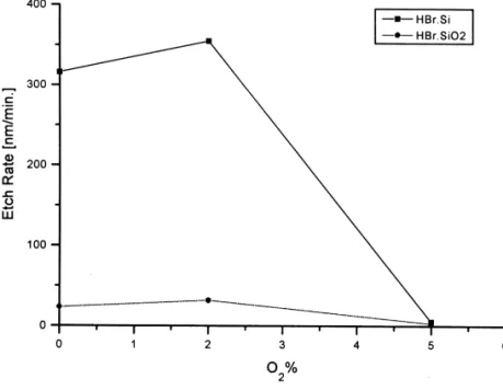
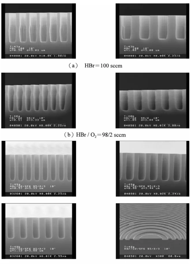
The etch rates were calculated based on 10-min etching and averaged over the entire etch time. As depicted in Fig. 1, the etch rate of silicon strongly depends on the percentage of O in HBr while that2 of SiO2 is weakly dependent on the O2 content. A small amount of oxygen (2%) enhances the concentration of etching species and thus increases the silicon etch rate. Nevertheless, the addition of 5% O creates too much oxide on the sidewall and bottom surface and results in the dramatic decrease2 in the etch rate. This leads to the decrease of etch selectivity of silicon over SiO2 with the O2 addition. Accordingly, 2% oxygen content recipe was selected for further improvement of the sidewall anisotropy with the SF addition. Fig. 2 shows the SEM micrographs of the etch profiles for various6 gas compositions. The feature size and etch depth are also displayed at the bottom of the figures. It was found through experimentation that a mixture of HBr / O / SF 595 / 2 / 3 sccm can yield a high2 6 degree of anisotropic etching with a good quality of etching surface.
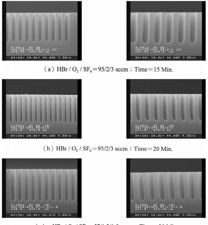
To investigate the RIE lag effect, the diffractive optical element etching was conducted for a long duration. Fig. 3a illustrates the results of a 15-min etching with a total flow rate of 100 sccm corresponding to a pressure of 3.3 mTorr. Anisotropic etch profile is preserved. However, as presented in Fig. 3b, the sidewall of submicron features has concave contour near the top surface when the etch depth exceeds about 5 mm. This is caused by the deflected ions. As a result, the total flow rate was reduced to 60 sccm to decrease the pressure to 2.2 mTorr. Although the etch rate diminishes, the vertical sidewall recovers, as shown in Fig. 3c.
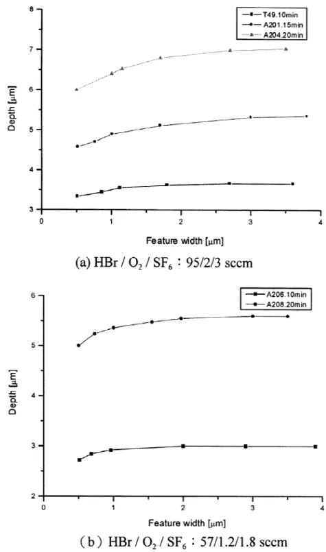
With depths and feature widths measured by SEM, Fig. 4a,b demonstrates the variation of depth with linewidth for total flow rates of 100 and 60 sccm, respectively. Since all Si zones were etched in a single run, one can interpret the depth variation as an etch rate variation, which increases with the linewidth. It is found that the depth variation is significant for submicron features while no notable depth change is observed for features above 3 mm. It also reveals that RIE lag will not occur until the aspect ratio is greater than about two. To obtain the regression relation of the etch depth versus zone width, a fourth-order polynomial was assumed:
2 3 4
d(w) 5 A 1 B*w 1 C*w 1 D*w 1 E*w (2)
where d and w are etch depth and zone width in mm, respectively. The results for each condition are demonstrated in Table 1. Then, the equation is valid through the zone width of about 2.5 mm. It is discovered that the coefficients E of the fourth-order terms are very small compared to other coefficients. Thus, the data points can be fitted by a third-order polynomial in w.
4. Conclusions
With the SiO layer as the etch hard mask, silicon was etched by a HBr-based chemistry. A small2 amount of oxygen (2%) increases the silicon etch rate while the addition of 5% O2 results in a dramatic decrease in the etch rate, and the etch rate of SiO is weakly dependent on the O content.2 2
Fig. 1. The effect of O content in HBr on the etch rate and selectivity (total flow rate, 100 sccm). (a) Etch rate of silicon2
and silicon dioxide and (b) etch selectivity of silicon over silicon dioxide.
This leads to a decrease of etch selectivity of silicon over SiO with the O addition. A high degree of2 2 anisotropic etching of silicon can be achieved by a mixture of HBr / O / SF 595 / 2 / 3 sccm. To ensure2 6 vertical sidewalls for submicron features with depth larger than 5 mm, working pressure needs to be reduced, which is realized by decreasing the total flow rate to 60 sccm.
Fig. 2. Etch profile for various gas compositions: (a) HBr5100 sccm, (b) HBr / O 598 / 2 sccm and (c) HBr / O / SF 595 /2 2 6
Fig. 3. Etch profile at different etch times and total flow rates: (a) HBr / O / SF 595 / 2 / 3 sccm, time515 min, (b)2 6 HBr / O / SF 595 / 2 / 3 sccm, time520 min; and (c) HBr / O / SF 557 / 1.2 / 1.8 sccm, time520 min.2 6 2 6
RIE lag was observed for an aspect ratio greater than about two. It was found that the lag effect is significant for submicron features while no notable depth change is observed for features above 3 mm in this study. The regression relation of the etch depth versus zone width was proved to be a third-order polynomial in zone width.
Fig. 4. Variation of depth with linewidth for different total flow rates: (a) HBr / O / SF 595 / 2 / 3 sccm; and (b)2 6
HBr / O / SF 557 / 1.2 / 1.8 sccm.2 6
Acknowledgements
This work was performed under the auspices of Opto-Electronics & Systems Laboratories, Industrial Technology Research Institute, under contract number 87S21-Q0.
Table 1
2 3 4
Regression relation of the etch depth versus zone width: d(w) 5 A 1 B*w 1 C*w 1 D*w 1 E*w , where d is etch depth and w is zone width in mm
Wafer Flow rate (sccm) Etch time A B C D E
no. HBr / O / SF2 6 (min) T49 95 / 2 / 3 10 3.0189 0.7452 20.3083 0.0453 25.65E-06 A201 95 / 2 / 3 15 4.0515 1.2228 20.4732 0.0716 21.0E-05 A204 95 / 2 / 3 20 5.4713 1.1670 20.2235 20.0015 1.27E-05 A206 57 / 1.2 / 1.8 10 2.2721 1.1854 20.6245 0.1071 21.4E-05 A208 57 / 1.2 / 1.8 20 4.0611 2.6708 21.7749 0.4155 22.6E-04 References
[1] Y.H. Lee, Z.H. Zhou, Feature-size dependence of etch rate in reactive ion etching, J. Electrochem. Soc. 138 (8, August) (1991) 2439.
[2] K.P. Muller, K. Roithner, H.-J. Timme, Selectivity and Si-load in deep trench etching, Microelectron. Eng. 27 (1995) 457–462.
[3] M.B. Stern, M. Holz, S.S. Medeiros, R.E. Knowlden, Fabricating binary optics: process variables critical to optical efficiency, J. Vac. Sci. Technol. B9 (6, Nov. / Dec.) (1991) 3117.
[4] M.B. Stern, S.S. Medeiros, Deep three-dimensional microstructure fabrication for infrared binary optics, J. Vac. Sci. Technol. B10 (6, Nov. / Dec.) (1992) 2520.
[5] M.G. Moharam, T.K. Gaylord, Rigorous coupled-wave analysis of dielectric surface relief grating, J. Opt. Soc. Am. 72 (1982) 1385–1392.
[6] A. Stemmer, H. Zarschizky, E. Knapek, G. lefranc, F. Mayerhofer, Efficiency enhancement of diffractive optical elements by variable relief profiling, Microelectron. Eng. 27 (1995) 171–174.
[7] H. Werlich, G. Sincerbox, B. Yung, Fabrication of high efficiency surface relief hologram, J. Imaging Technol. 10 (3) (1984) 105–115.