同時傳輸基頻資料以及微波訊號的光纖鏈結之研究
79
0
0
全文
(2) 同時傳輸基頻資料以及微波訊號的 光纖鏈結之研究. Study of Fiber-Optic Links Supporting Simultaneous Transmission of Baseband and Microwave Signals. 研究生 : 薛玉婷. Student : Yu-Ting Hsueh. 指導教授 : 祁甡 教授. Advisor : Prof. Sien Chi. 國 立 交 通 大 學 電 機 資 訊 學 院 光 電 工 程 研 究 所 碩 士 論 文. A Thesis Submitted in Partial Fulfillment of the Requirements for the Degree of Master in The Institute of Electro-Optical Engineering College of Electrical Engineering and Computer Science National Chiao-Tung University Hsinchu, Taiwan, Republic of China. July 2005 中華民國九十四年七月.
(3) 國. 立. 交. 通. 大. 學. 光電工程研究所 碩士論文. 同時傳輸基頻資料以及微波訊號的 光纖鏈結之研究 Study of Fiber-Optic Links Supporting Simultaneous Transmission of Baseband and Microwave Signals. 研究生 : 薛玉婷 指導教授 : 祁 甡 教授. 中 華 民 國 九 十 四 年 七 月.
(4) 同時傳輸基頻資料以及微波訊號的 光纖鏈結之研究. Study of Fiber-Optic Links Supporting Simultaneous Transmission of Baseband and Microwave Signals. 研究生 : 薛玉婷. Student : Yu-Ting Hsueh. 指導教授 : 祁甡 教授. Advisor : Prof. Sien Chi. 國 立 交 通 大 學 電 機 資 訊 學 院 光 電 工 程 研 究 所 碩 士 論 文. A Thesis Submitted in Partial Fulfillment of the Requirements for the Degree of Master in The Institute of Electro-Optical Engineering College of Electrical Engineering and Computer Science National Chiao-Tung University Hsinchu, Taiwan, Republic of China. July 2005 中華民國九十四年七月.
(5) 同時傳輸基頻資料以及微波訊號的 光纖鏈結之研究. 學生: 薛玉婷. 指導教授: 祁甡 教授. 國立交通大學光電工程研究所. 摘要 現在不管是有線或無線傳輸的頻寬需求量都在不停的增加,對於無 線訊號的存取,加載光纖射頻系統是一個極富彈性的傳輸方式,所以為 了低價的通訊建設,將固定的有線網路與加載光纖射頻系統結合在一起 是一個迫切的需求。於是,在本論文中,我們提出幾種可以同時傳輸基 頻以及微波訊號的光纖鏈結。其中,有兩種可以將 60GHz 頻帶中的射頻 訊號加在由頻移鍵控和差分相移鍵控調變的 10Gbps 基頻訊號上的架構 是利用 VPI 這套軟體來進行模擬分析,並且,靠著實驗以及模擬的結果 分 析 , 我 們 比 較 從 光 域 和 電 域 來 結 合 20GHz 頻 帶 的 射 頻 訊 號 和 2.488Gbps 基頻資料兩者之間的差異。希望我們提出的幾種架構可以有 益於光纖通訊系統的研究。. I.
(6) Study of Fiber-Optic Links Supporting Simultaneous Transmission of Baseband and Microwave Signals. Student: Yu-Ting Hsueh. Advisor: Prof. Sien Chi. Institute of Electro-Optical Engineering College of Electrical Engineering and Computer Science National Chiao Tung University. ABSTRACT. The demand on both wired and wireless access network is accelerating. For wireless access, one feasible option is radio over fiber (Rof). There is an emerging need to merge the fixed wired network and the RoF network for low cost infrastructure. So, in this thesis, several fiber-optic links that support simultaneous transmission of baseband data and radio signals are presented. By using simulation tool, VPI, we demonstrate two novel modulation methods which load 60-GHz-band radio signals on the frequency shift keying (FSK) and differential phase shift keying (DPSK) modulated 10Gbps baseband data, respectively. Moreover, two schemes which combine 20-GHz-band radio signals and 2.488Gbps baseband data in electrical and optical domain are compared through simulation and experimental results. These architectures are expected to be useful in the fields of fiber communication systems.. II.
(7) 致. 謝. Acknowledgements. 在這個猶如大家庭般的光纖通訊實驗室中,我順利的度過了兩年 的碩士生涯,其中,要特別的感謝祁甡老師給予我這個自由的環境學 習,還有常常給予我教導的陳智弘老師以及馮開明老師,您們總是這般 親切的與學生互動,讓我可以在碰到困難時能夠更放鬆的與您們討論, 進而學習到更多;並且也非常感謝撥空來擔任我口試委員的賴暎杰老 師,提出了許多寶貴的意見。 再來更要感謝的是實驗室的學長姐們,特別是負責指導我的彭煒仁 學長,謝謝您不厭其煩的教導我,給予我很多研究上的建議,才讓我可 以順利畢業;錢鴻章學長、彭朋群學長、黃明芳學姊、周森益學長、林 俊廷學長、項維巍學長、黃盈傑學長、林加和學長、陳志揚學長以及李 淑玲學姊您們平常對我的鼓勵和幫助,也讓我獲益不少,謝謝您們。 還有平時跟我一起打拼的實驗室夥伴們:倩伃、銘清、銘峰、金水、 裕民、淑惠、珮欣、小強、小鐵、重佑、光頭、叔叔、昇祐、小雨,雖 然我們是一群跨校又跨實驗室的組合,但是感情跟同一個實驗室的一樣 好呢,謝謝大家平時對我的照顧,讓我的研究所生涯多了很多快樂的回 憶。 最後,我要感謝我的家人和男友李昀,謝謝您們在情感上和經濟上 給我最大的支持,讓我可以專心的完成我的學業,我會繼續努力往人生 的下一個階段前進。. III.
(8) Contents. Acknowledgements…………………………………………………………I Abstract (Chinese)…………………………………………………………II Abstract (English)…………………………………………………...........III Contents…………………………………………………………………...IV List of Figures………………………………………………………........VII List of Tables……………………………………………………………….X. Chapter 1 Introduction 1.1 Preface……………………………………………………………..1 1.2 What is Rof ?.......................... ..................... ............1 1.2.1 Basic stracture……………………………………………..2 1.2.2 Network topology………………………………………….3 1.2.3 Various multiplexing schemes.………………………….3 1.3 Outline of the thesis…………………………………………………5. Chapter 2 Basic Component of a Fiber Optic Link 2.1. Introduction………………………………………………………...7. 2.2. RF-to-optical modulation device…………………………………..8 2.2.1 Optical source……………………………………………..9 2.2.2 Direct modulation and external modulation…………..….11 Optical transmission………………………………………………14 Optical-to-RF demodulation device………………………………16 2.4.1 Photodiodes………………………………………...........17. 2.3 2.4. IV.
(9) 2.5. 2.6 2.7. Noise characteristics………………………………………………18 2.5.1 Relatively intensity noise(RIN)………………………….19 2.5.2 Thermal noise…..………………………………………20 2.5.3 Shot noise……………………….……………………….21 Distortion characteristics………………………………………….22 Carrier-to-noise and distortion noise……………………………...24. Chapter 3 Simulations of Radio over Optical FSK and DPSK schemes 3.1 Introduction……………………………………………………….27 3.2 Simulation tool……………………………………………………28 3.3 Radio over optical FSK scheme…………………………………..28 3.3.1 Optical single-side band modulation….…………………30 3.3.2 Simulation results and discussion……………………32 3.4 Radio over optical DPSK scheme………………………………...38 3.4.1 DPSK demodulation…………...……………………….39 3.4.2 Simulation results and discussion………………………41 3.5 Discussion and comparison……………………………………….43 3.6 Future work……………………………………………………….44. Chapter 4 Hybrid Analog/Digital Fiber Links 4.1 Introduction…………………………………………………………..46 4.2 Hybrid analog/digital modulator and link………………………........46 4.2.1 Simulation and experimental results…………………….47 4.3 Hybrid analog/digital architecture using a DD-MZM………………..56 4.3.1 Simulation and experimental results…………………….57. Chapter 5 Conclusion V.
(10) 5.1. Summary of the thesis………………………………………………..60 5.1.1 Simulation of optical FSK and DPSK schemes……………...60 5.1.2 Hybrid analog/digital fiber links………………………61. Reference…………………………………………………………………...62. VI.
(11) List of Figures. Fig. 1-1 Basic structure of Radio-over-fiber system Fig. 1-2 Concept of Radio over fiber networks Fig. 1-3 Various network configurations Fig. 2-1 Basic components of a fiber optic link: modulation device, optical fiber, and photodetection device Fig. 2-2 Components of an optical transmitter Fig. 2-3 (a) Diagram showing the principal components of FP-LD (b) Idealized spectral output of FP-LD Fig. 2-4 (a) DFB laser structure (b) Idealized spectral output of DFB-LD Fig. 2-5 Schematic optical power versus current characteristic of a laser diode Fig. 2-6 (a) Diagram showing the layout of a typical MZM (b) MZM optical transfer function Fig. 2-7 Typical loss vs. length of coax and optical fiber links operating at 10GHz Fig. 2-8 Loss vs. wavelength for silica optical fiber and the wavelength ranges of some common electro-optic device materials Fig. 2-9 Components of an optical receiver Fig. 2-10 Structures of three photodiodes together with the electric-field distribution under reverse bias (a) p-n photodiode (b) p-i-n photodiode (c) APD photodiode Fig. 2-11 Receiver equivalent circuit with signal and noise current sources Fig. 2-12 Caculated RIN spectra at several power levels for a typical 1.55um semiconductor laser Fig. 2-13 Circuit representation of a physical, noisy resistor (a) and equivalent circuits for the thermal noise of the resistor: (b) voltage source in series with a noiseless. VII.
(12) resistor and (c) current source in parallel with a noiseless resistor Fig. 2-14 Plot of the output signal powers - fundamental, second- and third-order intermodulation - as a function of the inpur signal power. Fig. 2-15 CNR, CTB and CSO in RF subcarrier system Fig. 3-1 The proposed radio over optical FSK scheme Fig. 3-2 The DD-MZM configuration Fig. 3-3 The FSK simulation diagram Fig. 3-4 (a) The laser chirp and output power characteristics related to input current. (b) The EA modulator relative output power vs. driving voltage. Fig. 3-5 (a) The output eye diagram after laser (b) Eye diagram after EA compensation Fig. 3-6 (a) Optical spectrum of EA output. (b) Output spectrum of SSB DD-MZM. Fig. 3-7 Optical spectrum after the optical filter Fig. 3-8 The carrier to noise and distortion ratio in both scheme cases with and without EAM Fig.3-9 Comparison of the spectrums with and without EAM Fig. 3-10 (a) Probability of error of the received baseband data (b) The eye diagrams of the schemes with and without EAM at BER = 10-9 Fig. 3-11 The simulation setup of DPSK scheme Fig. 3-12 A typical DPSK receiver Fig. 3-13 (a)The spectrum of DI (b) The spectrum of narrow band filter (c) 10Gbps NRZ-DPSK signal spectrum at the input and output of BPF Fig. 3-14 (a)Probability of error of the received baseband data (b)Eye diagrams before and after filter at BER=10-9 in back to back situation. Fig. 3-15 CNDR vs. OMI for DPSK and FSK schemes Fig. 3-16 Receiver sensitivities for DPSK and FSK schemes Fig. 3-17 Hybrid passive WDM-TDM / radio distribution network VIII.
(13) Fig. 4-1 (a) A hybrid mode modulator combines radio and baseband signals in electrical domain. (b) A hybrid mode modulator combines radio and baseband signals in optical domain. Fig. 4-2 System setup for simulation and experiment Fig. 4-3 CNDR vs. OMI in both scheme cases experimentally Fig. 4-4 CNDR vs. OMI in both scheme cases by simulation Fig. 4-5 Reflection optical spectrum of FBG Fig. 4-6 (a) Optical spectrum before FBG (b) Optical spectrum after FBG Fig. 4-7 Bit error rate of baseband data in both schemes with two radio signals located at their respective optimum OMI. Fig. 4-8 (a) Bit error rate of baseband data in scheme-1 with different OMI (b) Bit error rate of baseband data in scheme-1 with different OMI Fig. 4-9 System setup for simulation and experiment Fig. 4-10 CNDR vs. OMI in different ER of baseband data in experiment Fig. 4-11 (a) BER of baseband data with different OMI in experiment (b) BER of baseband data with different OMI in simulation. IX.
(14) List of Tables. Table 1-1 Features of different network configurations Table 1-2 Performance comparison of various multiplexing schemes Table 2-1 Comparison of MMF and SMF in cable parameters Table 3-1 Three types of optical modulation Table 4-1 Comparison of optical received power with different OMI in experiment and simulation. X.
(15) Chapter 1 Introduction. 1.1 Preface Envisioning a global village, people need to transmit and receive messages at anywhere, any time. In addition, the explosive growth in Internet applications, such as World Wide Web, indicates the enormous increase in bandwidth and low power that the coming world of multimedia interactive applications will require from future networks. So the demands on wireless and wired line capacity are increasing. Facing the huge capacity, one of the best solutions is using fiber as the transmission medium. The wireless signals are proposed to be carried on the optical domain as radio over fiber (Rof) [1], [2]. There is an emerging need to merge the fixed wired network and the Rof network for low cost infrastructure. So, in the thesis, we mainly study how to simultaneously transmit digital and analog signals.. 1.2 What is Rof ? The development of optical fiber technology in wireless networks provides great potential for increasing the capacity and Quality of Service (QoS) without largely occupying additional radio spectrum. Radio over fiber systems have many clear advantages such as better coverage, higher capacity, lower cost, lower power, and easier installation. Therefore, Rof technology is the most suitable candidate for indoor applications such as office blocks, shopping malls, airport terminals, and large offices, in addition to outdoor applications such as those underground, tunnels, narrow streets (i.e., dead zone areas ), and highways. In addition to the above-mentioned advantages, Rof technology has the additional benefit that transferring the RF frequency allocation to a. 1.
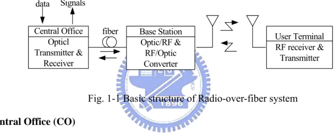
(16) central station can allow flexible and mobile network channel allocation and rapid response to variations in traffic demand. Thus it can be seen that Rof technology is an important communication issue in the future.. 1.2.1 Basic structure Rof is an analog optical link transmitting modulated RF signals. It serves to transmit the RF signals downlink and uplink, i.e. to and from central office (CO) to base stations (BS) using optical fiber before transmitted to user terminals by antennas, as indicated in Fig. 1-1. data. Signals. Central Office Opticl Transmitter & Receiver. fiber. Base Station Optic/RF & RF/Optic Converter. User Terminal RF receiver & Transmitter. Fig. 1-1 Basic structure of Radio-over-fiber system Central Office (CO) A remote central office, or called the radio control station, executes most of troublesome signal processing such as including coding, multiplexing, RF generation, modulation, demodulation and so on. It provides a much simplified and cost-effective radio access network and promises easy realization of recent advance demodulation techniques, such as macro-diversity and handover control. Base Station (BS) The design of BS is very simple; a BS only includes optical-electrical (O/E) and electrical- optical (E/O) converters, an antenna and some microwave circuitry. The radio signals converted into optical signals are transmitted via a fiber optic link with the benefit of its low transmission loss. Therefore, the architecture of fiber optic radio access links can be independent of the radio signal format and can provide many universal radio 2.
(17) access links that are available to any type of radio signal. This means that such radio access links are very flexible to modification of radio formats or the opening of new radio services [1]. User Terminal (UT) At UT, The RF signals can be transmitted or received through antennas or mobile interface and so on. Because increased traffic and propagation properties of millimeter waves require small cells and millimeter wave circuits are rather expensive, the cost of base stations will be a determining role. A simple BS means small and light enclosures (easier and more flexible costs) and low cost (in terms of equipment cost and maintenance cost). Centralization brings on many benefits such as equipment sharing, and dynamic resource allocation, and more effective management. In Fig. 1-2, we can see the concept of Radio over fiber access networks.. Routing node. Control Station. Fig. 1-2 Concept of Radio over fiber networks. 1.2.2 Network topology There are three ways under consideration for the link configuration topology in radio highway networks. They are star configuration, ring configuration, and bus configuration, 3.
(18) as indicated in Fig. 1-3. E /O E /O. E /O. E /O. E /O E /O. E /O. E /O. S t a r c o n f ig u r a t io n. B u s c o n f ig u r a t io n E /O. E /O. E /O E /O. R in g c o n f ig u r a t io n. Fig. 1-3 Various network configurations. These configurations have their own benefits and shortcomings. The features are summarized in Table 1-1. In constructing fiber optic radio access networks, easy extension of BSs is important, because the density of BSs increases according to the the number of users. For indoor use, they are critical to flex the network easily and to reduce the fiber count are critical, because the reinstallation of fibers is wasteful. Therefore, we choose the bus or star network configuration. The difference between them is whether to terminate at a certain BS in the network. Network configuration. advantage. disadvantage. Star configuration. *easy maintenance *high reliability *simple construction. *difficult to construct or extend *difficult to increase the number of BSs. Bus configuration. *reduce the fiber counts by quite a bit *easy extension of BSs. *difficult to maintain. Ring configuration. *offer cost-effective and quick construction. *difficult to maintain. Table 1-1 Features of different network configurations 4.
(19) 1.2.3 Various multiplexing schemes The candidates for multiplexing schemes are TDMA, SCM, FDMA, CDMA, and WDMA. The ease of use, the simplicity of network construction, and the cost efficiency are important points when discussing which multiplexing schemes is suitable for radio access networks. The characters of these schemes are summarized in Table 1-2.. 1.3 Outline of the thesis In this thesis, the motivation of the study and the fundamental concept of Radio over fiber (Rof) are given in Chapter 1. In Chapter 2, we introduce some basic optical components used in fiber optic communication system, such as optical transmitter, fiber, optical receiver. Simultaneous transmission of 60-GHz-band radio signals and 10-Gbps baseband data in two different schemes, one is FSK architecture and the other is DPSK architecture, is simulated using a commercial tool, VPI. The comparison between the two schemes and analysis are given in Chapter 3. In Chapter 4, we demonstrate two possible schemes which combine two radio signals and baseband data in electrical and optical domains for experiment and simulation. And we will compare the results of the two architectures with the performance of the DD-MZ scheme. Finally, we concluded the study in Chapter 5.. 5.
(20) Multiplexing Scheme. Advantage. Disadvantage. TDMA. *intermodulation/direct detection link *configuration is allowed *easy photonic routing *no generation of optical beat noise. *demand of fast photonic switching *demand of time synchronization control among BSs. SCM. *intermodulation/direct detection link *configuration is allowed. *occurrence of optical beat noise *radio signals must be FDM format *photonic routing is impossible. FDMA. *effective utilization of optical frequency *robustness to fiber dispersion *high receiver sensitivity. *demand of coherent detection *demand of very narrow optical and frequency shifter for photonic routing. CDMA. *Easy realization of random access. *demand of fast code synchronization *demand of much fast operation of photonic device for coding *feasibility of photonic routing is unknown. TDMA. *intermodulation/direct detection link *configuration is allowed. *demand of many wavelengths *demand of many wavelength filters and wavelength converter for photonic routing -. Table 1-2 Performance comparison of various multiplexing schemes. 6.
(21) Chapter 2 Basic Components of a Fiber Optic Link. 2.1 Introduction An optical link is defined as consisting of all the components required to carry an electrical signal over an optical carrier such as modulation device, optical transmission, and demodulation device. The diagram is shown in Fig. 2-1. At the input end, there is a modulation device, which impresses the electrical signal onto the optical carrier. An optical fiber couples the modulation device output to the input of the demodulation device, which converts the optical signal to the electrical signal. Since the objective of an optic link is to reproduce the RF signal at the receiver, the link can convey a wide variety of signal format. In some applications the RF signal is an unmodulated carrier-as for example in the distribution of local oscillator signals in a radar or communication system. In other applications the RF signal consists of a carrier modulated with an analog or digital signal. O p tic a l-to -R F D e m o d u la tio n D e v ic e. R F -to -O p tic a l M o d u la tio n D e v ic e. RF o u tp u t. O p tic a l T ra n sm issio n. Fig. 2-1 Basic components of a fiber optic link: modulation device, optical fiber, and photodetection device For the modulation device we will use a diode laser and for the demodulation device a photodiode. The former converts a RF signal into a corresponding optical intensity while the latter does the reverse – it recovers the RF signal from the optical carrier. And we connect the two devices optically via optical fiber. The sources of optical signals and the optical detector are key components for a fiber optic link. The main requirements of. 7.
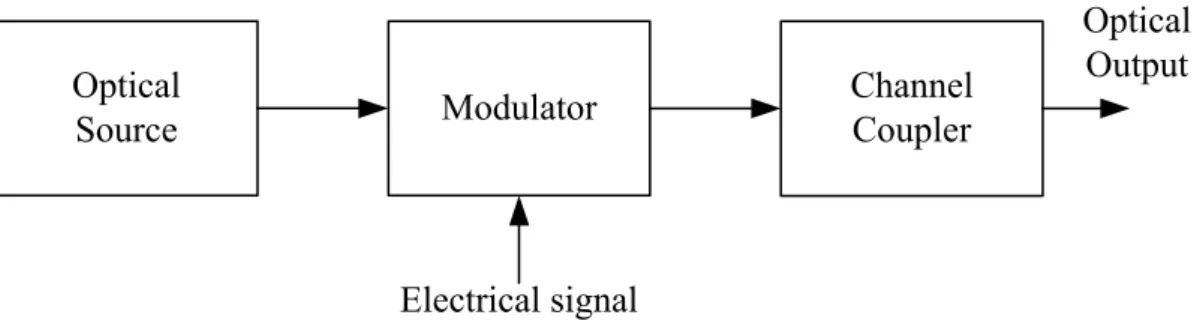
(22) the diode laser are wavelength stability with time and temperature, ease of control, manufacturability, reliability, and low cost. And for receiver node, optical networks employ high sensitivity photodetectors together with adequate amplification and electrical processing to provide the best recovery of the transmitted data. In the next section we will discuss the design of modulation device and demodulation device and the role of optical fiber as a communication channel.. 2.2 RF-to-optical modulation device An optical transmitter applications in aimed at converting the electrical signal into optical carrier and launching the optical signals into the optical fiber. It is composed of an optical source, a modulator, and a channel coupler. The block diagram is shown in Fig. 2-2. In optical fiber communication channel, semiconductor lasers or light emitting diodes (LED) are the most common optical sources. Different modulators are used to impressing the electrical signals onto the optical carrier. The ways of modulation are divided into direct modulation and external modulation. Both of these will be described in detail. The coupler is typically a microlens that focuses the optical signal on the entrance plane of an optical fiber with the maximum possible efficiency.. Optical Source. Modulator. Channel Coupler. Electrical signal Fig. 2-2 Components of an optical transmitter. 8. Optical Output.
(23) 2.2.1 Optical source Light-emitting diodes A forward-biased p-n junction emits light through spontaneous emission, a phenomenon referred to as electroluminescence. The emitted light is incoherent with a relatively wide spectral width (30-60 nm) and a relatively large angular spread. The advantages of LED are cheap and simple. It is limited by low output power, broad bandwidth, frequency response ~ 100MHz, and transmission length. Semiconductor lasers The difference between the LED and the semiconductor laser is the way of emission. Semiconductor lasers emit light through stimulated emission. The characteristics of this emission are high output power and the coherent nature of emitted light. And a relatively narrow angular spread of the output beam can increase the coupling efficiency (~ 50%). Furthermore, the narrow spectral width of emitted light allows operation at high bit rates (~10Gb/s). Semiconductor lasers are divided into single-mode laser such as the distributed feedback laser diode (DFB-LD) and multimode laser such as the Fabry-Perot laser diode (FP-LD). The principal parts of FP-LD are a p-n diode junction and an optical waveguide with partially reflecting mirrors at either end. The diagram is shown in Fig. 2-3(a). In a Fabry-Perot cavity, with a vacuum between the mirrors, resonances exist for any wavelength, λ0, which after reflections off of both of the mirrors are again in phase with the original wave. The condition for resonant wavelength of a FP-LD cavity can be expressed as 2l = mλ0 ,. (2-1). where l is the distance between two mirrors and the integer m represents the number of mode. The wavelength spacing between two adjacent longitudinal modes (m and m+1) within the cavity, ∆λ, is approximated by 9.
(24) ∆λ ≈. λ2 2l. .. (2-2). When the cavity is formed in a semiconductor with index of refraction n, we substitute λ = λ0/n in Eq. 2-2; the result is ∆λ0 ≈. λ2 2nl. .. (2-3). The cavity length is typically in the order of hundred micrometers, much larger than the lasing wavelength, so that many longitudinal may exist simultaneously. The spectral plot of FP-LD is shown in Fig. 2-3 (b). The characteristics of FP-LD are low threshold current, high power output [18-19], and high relative intensity noise (RIN) because of mode competition [20-21].Single mode lasing is hard to achieve in FP structure, especially under modulation. Dynamic single mode operation is required in many applications and it is achieved using optical cavities with selective reflection. C urrent. M etal C ontact. p-T Y P E. A ctive L ayer. C leaved F acet. n-T Y P E. (a). P L,O. ∆λ. (b). λ. Fig. 2-3 (a) Diagram showing the principal components of FP-LD (b) Idealized spectral output of FP-LD. 10.
(25) The feedback in distributed feedback (DFB) lasers, as the name implies, is not localized at the facets but is distributed throughout the cavity length. This is achieved through an internal built-in grating that leads to a periodic variation of the mode index. Feedback occurs by means of Bragg diffraction, a phenomenon that couples the waves propagating in the forward and backward direction. The diagram of a DFB laser structure and spectral output is shown in Fig. 2-4. In practice the dominant lasing mode is 20dB above the residual modes. The DFB laser is widely used for single mode applications [21].. Grating. p-TYPE. Active layer. n-TYPE (a). Dominant Lasing Mode. PL,O. Residual Modes. (b). λ. Fig. 2-4 (a) DFB laser structure (b) Idealized spectral output of DFB-LD. 2.2.2 Direct modulation and external modulation Two types of transmitter have been developed: intensity modulated semiconductor laser and external modulator. The former has the advantages of being simple, compact, and low cost. On the other hand, the external modulator offers higher power and low 11.
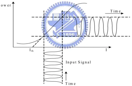
(26) chirp. Therefore, the external modulator is widely used in optical amplified trunk systems that need higher power budgets and super performance [22-23]. With direct modulation, the modulation signal directly changes the intensity of the laser output. Both LEDs and semiconductor lasers can be directly modulated using analog and digital signals. In Fig. 2-5, laser diode characteristic are revealed together with characteristic quantities. Output optical power versus current can be given as. Popt ( I ) =. hf η L ( I − I th ) , e. (2-4). where h is Plank’s constant, f is the optical carrier frequency, e is the charge of the electron, and ηL is the quantum efficiency of the laser diode which is the average number of generated photons per electron. P ow er T im e. I th. I. In p u t S ig n a l. T im e. Fig. 2-5 Schematic optical power versus current characteristic of a laser diode. Although this modulation is simpler and cheaper, its applications are limited by some reasons. The first one is bandwidth: the useful bandwidth of modulation is restricted to the range from DC to the laser relaxation resonance. Further, it can cause relatively long and undesired transients during ON–OFF switching and are accompanied by an equally undesired frequency chirping [24]. This chirping phenomenon results in. 12.
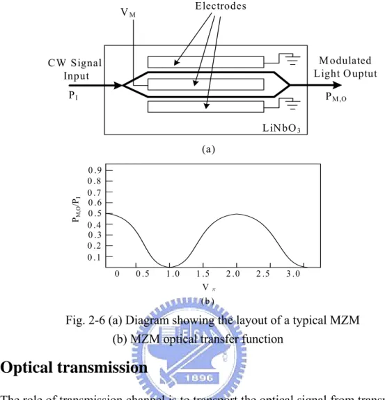
(27) frequency modulation superimposed on the (wanted) intensity modulation. In recent years, by improving the drawbacks, some lasers with modulation cutoff frequencies up to about 40GHz have been reported [25]. For external modulation, the laser operates at a constant optical power (CW) and the desired intensity modulation of the optical carrier is introduced via a separate device – optical modulator. External optical modulator functioning is based on at least three principles: electro-optical, electroabsorption, and interferometric modulators. The modulator based on a Mach-Zehnder interfernometer is the most popular because of its analytic tractability. The Mach-Zehnder modulator (MZM) is fabricated on a slab of lithium niobate (LiNbO3). The waveguide is created using a lithographic process similar to that used in the manufacturing of semiconductors. The waveguide region is slightly doped with impurities to increase the index of refraction so that the light is guided through the device. Fig. 2-6 shows the layout of a typical MZM and MZM optical transfer function PM,O/PI versus Vπ for the case where the ratio PM,O/PI = 0.5 when the modulator is biased for maximum optical transmission. Vπ is the voltage to induce 180 degrees, or π radians of phase shift between the two optical waves at the output combiner. External modulation is typically used in high-speed applications such as long-haul telecommunication or cable TV head ends. The benefits of external modulation are that it is much faster and can be used with higher-power laser sources. The disadvantage is that it is more expensive and requires complex circuitry to handle the high frequency RF modulation signal.. 13.
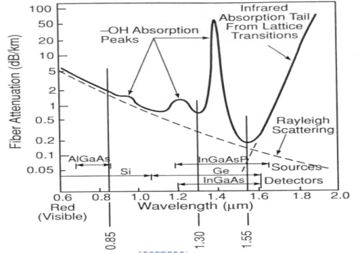
(28) Electrodes. VM. M odulated Light O uptut. CW Signal Input PI. P M ,O LiN bO 3. PM,O/PI. (a) 0 .9 0 .8 0 .7 0 .6 0 .5 0 .4 0 .3 0 .2 0 .1. 0. 0 .5. 1 .0. 1 .5 2 .0 Vπ. 2 .5. 3 .0. (b ). Fig. 2-6 (a) Diagram showing the layout of a typical MZM (b) MZM optical transfer function. 2.3 Optical transmission The role of transmission channel is to transport the optical signal from transmitter to receiver without distorting it. Most lightwave systems choose optical fibers as the communication channel because fiber can transmit light with a smaller amount of power loss than coax cable. An example of this is shown in Fig. 2-7.. Fig. 2-7 Typical loss vs. length of coax and optical fiber links operating at 10GHz (Ref. Charles H. Cox. III, Analog optical links, 2004) 14.
(29) One of the fiber’s key wavelength parameters is optical loss. Fig. 2-8 is a plot of the loss vs. wavelength for a typical, silica-based optical fiber. From the figure, we know there are several factors contribute to the loss. The two most important among them are OH absorption and Rayleigh scattering. More recent fibers have virtually eliminated the dominant OH absorption peak between 1.3 and 1.55 µm.. Fig. 2-8 Loss vs. wavelength for silica optical fiber and the wavelength ranges of some common electro-optic device materials (Ref. Charles H. Cox. III, Analog optical links, 2004) The result of combining the device and fiber constraints is that there are three primary wavelength bands that are used in fiber optical links. In most cases this light will are located in bands around 1.3 and 1.55 µm. Fig. 2-8 shows that the best wavelength is the band around 1.55 µm, where the lowest loss is. However, the band around 1.3 µm has also been used extensively because originally this was the only band where the chromatic dispersion is zero. The chromatic dispersion is important parameter for high frequency or long distance transmissions. At 1.55 µm, the chromatic dispersion is typically 17 ps/(nm km). 15.
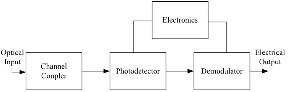
(30) There are two types of typical optical fibers, one is single-mode fiber (SMF) and the other is multi-mode fiber (MMF). The core of a single mode fiber is so small, typically ~5 to 8 µm in diameter. Single-mode fibers support on the fundamental mode of the fiber. The fiber is designed such that all higher-order modes are cut off at the operating wavelength. A multi-mode fiber has larger core, typically 50 to 62 µm in diameter, permits multiple light paths to propagate down the fiber. The larger core makes for more efficient fiber to device coupling than is possible with single-mode fiber. However, multi-mode fibers have a problem – mode dispersion. The multiple modes travel different paths and consequently have different propagation times through the fiber, i.e. different propagation velocities for the different modes. At the system asked for high performance, single-mode fiber is the choice. At Table 2-1 provides a quick reference guide to cable parameters [26].. Graded index MMF. Step-index SMF. Application. Used in LAN applications. Used in backbone or long-haul applications. Loss. Moderate loss (-3dB/km or 1dB/km). Very low loss (-0.35 dB/km or 0.20dB/km). Wavelength. Operates @ 1310/1550 nm. Operates @ 820/1310/1550 nm. Table 2-1 Comparison of MMF and SMF in cable parameters. 2.4 Optical-to-RF demodulation device The receiver is designed to convert the optical signal back into electrical form and recover the data transmitted through the lightwave system. Fig. 2-9 shows the components of an optical receiver. Its main component is a photodetector, which is used to convert light into electricity (photocurrent) through the photoelectric effect. The requirements for a photodetector are high sensitivity, fast response, low noise, low cost, 16.
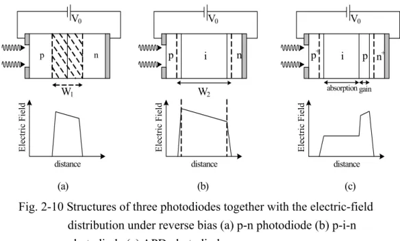
(31) and high reliability. The detector determines the performance of fiber-optic links.. Electronics. Optical Input. Channel Coupler. Electrical Output Photodetector. Demodulator. Fig. 2-9 Components of an optical receiver. 2.4.1 Photodiodes The basic concept of photodetector is optical absorption. If the energy hν of incident photons exceeds the bandgap energy, an electorn-hole pair is generated each time a photon is absorbed by the semiconductor. Under the influence of an electric field set up by an applied voltage, electrons and holes are swept across the semiconductor, resulting in a flow of electric current. The photocurrent Ip is directly proportional to the incident optical power Pin, i.e.,. I p = RPin ,. (2-5). where R is the responsibility of the photodetector.. R=. ηq (in units of A/W), hν. (2-6). where η is the quantum efficiency and defined as η=. electron generation rate . photon incidence rate.. (2-7). We introduce three types of photodetectors—p-n photodiode, p-i-n photodiode, and avalanche photodiode (APD). These structures and the electric-field distribution under reverse bias of three types are shown in Fig. 2-10.. 17.
(32) V0 p. V0 p. n. distance. (a). p+. n. p n+. i. absorption gain. W2 Electric Field. Electric Field. Electric Field. W1. i. V0. distance. (b). distance. (c). Fig. 2-10 Structures of three photodiodes together with the electric-field distribution under reverse bias (a) p-n photodiode (b) p-i-n photodiode (c) APD photodiode. In order to increase the depletion-region width of a p-n photodiode, p-i-n photodiode insert a layer of undoped (or light doped) semiconductor material between the p-n junction. However, the responsibility of p-i-n photodiodes is limited and takes its maximum value R = q/hν for η =1. APDs can have much larger values of R, as they are designed to provide an internal current gain (known as impact ionization) in a way similar to photomultiplier tubes. The advantage of APDs is less total optical power requirement. But the thermal noise would increase.. 2.5 Noise characteristics There are three dominant noise sources in a link: thermal, shot, and relative intensity noise (RIN). Fiber-optic links typically exhibit a significant amount of signal loss, but the noise is generally much less than above noise; thus, it can be neglected. Each noise source obeys a different law, i.e. all noise sources are independent. We can represent the total noise power by summing the independent noise power. Fig. 2-11 shows the. 18.
(33) equivalent circuit of the PIN direct receiver. <isg2>. R0. Output current R <irin2>. <ish2>. <ith2>. Fig. 2-11 Receiver equivalent circuit with signal and noise current sources. 2.5.1 Relative intensity noise (RIN) Laser noise arises from random fluctuations in its intensity, phase, and frequency even when the laser is biased at constant current with negligible current fluctuations. The two fundamental noise sources are spontaneous emission and electron-hole recombination. The dominated noise source is spontaneous emission which perturbs the coherent field by adding random amplitude and phase. The laser noise measured directly at the transmitter is often referred to as relative intensity noise (rin) which defined as. rin =. 2 < Prin (t ) 2 > , < P0 > 2 ∆f. (2-8). where P0 is the total optical power and the factor of 2 in the frequency domain expression comes from integrating the effects of both positive and negative frequencies. After detection, the optical power has been converted to an electrical current. So we can write Eq. 2-8 in terms of photodiode currents:. rin =. 2 < I rin (t ) 2 > , < I D > 2 ∆f. (2-9). where ID is the average received photocurrent. Relative intensity noise of laser is usually specified in terms of RIN in dB/Hz:. RIN = 10 log10 rin .. (2-10). The RIN frequency spectrum is no flat over all the frequencies of interest in links 19.
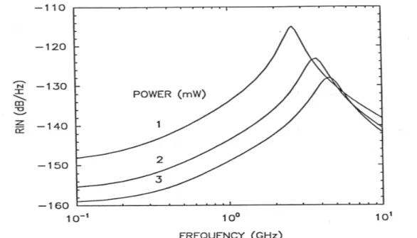
(34) and hence this is not a white noise source. Fig. 2-12 shows the calculated RIN spectrum at several power levels for a typical 1.55 µm InGaAsP laser. The RIN spectrum is almost constant at low frequencies, peaks at the relaxation resonance frequency and then falls above resonance. However, most links analyses assume that RIN is a constant within the bandwidth of interest. To measure the RIN, first the optical power is converted to a current after the detector and the noise of this photocurrent may be easily observed by using an RF spectrum analyzer.. Fig. 2-12 Caculated RIN spectra at several power levels for a typical 1.55um semiconductor laser (Ref. Govind P. Agrawal, Fiber-Optic Communication Systems, 1997). 2.5.2 Thermal noise At a finite temperature, electron carriers move randomly in conductors. Random thermal motion of electrons in a resistor manifests as a fluctuating current even in the absence of an applied voltage. This additional noise component is referred to as thermal noise, which was reported experimentally and theoretically by Johnson (1928) [27] and Nyquist (1928) [28] in Physical Review. Nyquist showed that the mean-square value of the noise voltage <vt2> across a resistor R at an absolute temperature T as measured in a 20.
(35) effective noise bandwidth ∆f is given by 2. < vt >= 4kTR∆f ,. (2-11). Where k is Boltzmann’s constant, which has a value of 1.38 × 10⁻²³ J/K. The temperature used in calculating the noise is the physical temperature of the loss, which is usually the physical temperature of the component. We can use the circuit impacts to analyze the thermal noise, replacing the noisy, physical resistors, as shown in Fig. 2-13(a), by noiseless resistors with the same resistance as the physical resistors that are connected in series with voltage sources; see Fig. 2-13(b). From elementary circuit theory we know that the circuit in Fig. 2-13 (c) is equivalent to the circuit shown in Fig. 2-13(b), provided that the mean-square current is 2. < it >= 4kT∆f / R .. (2-12). R NOISELESS R NOISY. (a). <v t2 >. <i t2>. (b). R NOISELESS. (c). Fig. 2-13 Circuit representation of a physical, noisy resistor (a) and equivalent circuits for the thermal noise of the resistor: (b) voltage source in series with a noiseless resistor and (c) current source in parallel with a noiseless resistor. 2.5.3 Shot noise Shot noise is a manifestation of the fact that the electric current consists of a stream of electrons that are generated at random times. The theoretical basis for this noise was. 21.
(36) established by Schottky (1918). The photodiode current generated in response to a constant optical signal can be written as. I (t ) = I p + i s (t ) ,. (2-13). where Ip=RPin is the average current and is(t) is a current fluctuation related to shot noise. The shot noise is represented by a mean square shot noise current generator, 2. < i s >= 2qI p ∆f ,. (2-14). where ∆f is the effective noise bandwidth. The same bandwidth appears in the case of both shot and thermal noises.. 2.6 Distortion characteristics In above section, we explored one type of extraneous signals in links – noise. In this section, we will investigate the other type of extraneous signals in links – distortion. Unlike noise however, distortion signals are deterministic. We begin as assuming that the modulation is a pure sinusoid. It generates light power modulations at the input frequency ω and also at the harmonics 2ω, 3ω, ···, nω. Harmonic distortion (HD) depends on the nonlinearity of a transmission system. The amplitude of the nth order harmonic is proportional to the nth power of the optical modulation index (OMI) and it decreases rapidly with higher order. The optical modulation is defined as m≡. ∆I ∆P = ^ , I b − I th P. (2-15). where ∆I is the variation of electrical driving current around a bias point in modulating a laser light source, Ib is the laser bias current, and Ith is the laser threshold current. For a far common RF practice, two equal-amplitude sinusoids are used to characterizing distortion. The harmonic terms for each frequency are of course identical to the single harmonic term. However, when two frequencies are presented 22.
(37) simultaneously, additional distortion terms are generated. These are referred to as the intermodulation distortion. Two signals at ω1 and ω2, for example, are accompanied by second order distortions are frequencies 2ω1,2, ω1±ω2, and third order distortions at frequencies 3ω1,2, 2ω1±ω2, and 2ω2±ω1, etc. The third order modulation distortion (IMDs) at 2ω1-ω2 and 2ω2-ω1 are special interest since they are close to original signals and they might interfere with other signals in multichannels applications. The third order IMD increases as the cube of the OMI [29]. The power at which the fundamental and one of the distortion curves intersect is one measure of distortion. As we will see below, practical systems are always operated below this point to avoid serious distortion, but the intersection point is a useful measure of system performance. Clearly the higher the intercept point, the lower the distortion at a given power. In general there will be a separate intercept point for the second-order, IP2, and third-order, IP3, distortions, as shown in Fig. 2-14. In this figure, we can find another measure of distortion–intermodulation-free dynamic range (IM-free DR). It is also called spurious free dynamic range (SFDR). The IM-free DR is the function of both distortion and the noise of the component. Thus to define the IM-free DR we need to add the noise power to Fig. 2-14. In multichannel applications such as CATV and cellular telephone, multiple, regularly spaced carriers are frequency multiplexed onto the optical link. In such cases, these multiple signals can interfere and add to levels that are greater than simple power addition, so there is a need for a new distortion measure that makes statistical assumptions. The common measures that are often used are composite second order (CSO) and composite triple beat (CTB) quantities.. 23.
(38) Fig. 2-14 Plot of the output signal powers - fundamental, second- and third-order intermodulation - as a function of the inpur signal power. (Ref. Charles H. Cox. III, Analog optical links, 2004). 2.7 Carrier-to-noise and distortion ratio An RF lightwave system consists of transmitters, fiber link, and receivers. The performance of this system is determined by the performance of those active and also passive components. All these can be quantified by carrier-to-noise ratio (CNR), and second and third order distortion (CSO and CTB). This is shown in Fig.2-15.. Fig. 2-15 CNR, CTB and CSO in RF subcarrier system (Ref. William S.C. Chang, RF Photonic Technology in Optical Fiber Links, 2002) 24.
(39) We can also combine these measures as carrier-to-noise-and-distortion ratio (CNDR) which directly determines the received signal quality at customer premises equipment. CNDR is described as CNDR −1 = CNR RX. −1. −1. + CNR sh + CNR RIN. −1. + CDRCTB. −1. + CDRcl. −1. (2-16). The first three terms on the right of this equation represent the CNRs by receiver noise, shot noise, and RIN, respectively. These three terms can be written as m2 I0. CNR RX =. CNRsh =. 2. (2-17). 2. 2 B < nth >. m2 I0 4eBM. CNR RIN =. (2-18). m2 2 RIN ⋅ BM. (2-19). where m I0. optical modulation index (OMI); photocurrent from the signal source;. < i 2 RX > B q. thermal noise of the receiver; noise bandwidth; electrical charge;. RIN. relative intensity noise of the optical sources.. The fourth term on the right of Eq.(2-16) represents the carrier-to-distortion ratio (CDR), which can be written as [30] CDRCTB =. IP3. 2. 4 N IM 3 Pin. (2-20). 2. where N IM 3 Pin IP3. number of third-order intermodulation tones; input RF power; input third-order intercept point.. In this equation, we ignored the second-order intermodulation term since most fiber optic networks for transporting wireless signals utilize less than one octave of bandwidth. Thus for N carriers, the number of intermodulation tones at the kth subcarrier can be described 25.
(40) as N IM 3 =. 1 1 k ( N + k − 1) + {( N − 3) 2 − 5} − {1 − (−1) N }(−1) N + k 2 4 8. (2-21). where k=1 represent the first channel [30]. The highest number of intermodulation terms, which falls on the center of the signal band be comes to be (3N2-14N+8)/8. The last term on the right of Eq.(2-16) represents CDR degradation due to clipping distortion which occurs when the bias current falls below threshold current instantaneously [31]. It can be expressed as CDRcl =. 2π (1 + 6µ 2 ). µ. 3. exp(. 1 2µ 2. ). (2-22). where μis the total rms modulation index m(N/2)1/2. The clipping distortion becomes important when the total rms modulation index is greater than ~25%.. 26.
(41) Chapter 3 Simulations of Radio over Optical FSK and DPSK Schemes. 3.1 Introduction The demand on broadband services in both fixed and wireless access network is increasing. The millimeter-wave band is considered to be a promising solution because of its spectrum availability, compact size of radio frequency (RF) devices. There is an emerging need to integrate the fixed wired network and the Rof wireless network with low cost infrastructure. Simultaneous transmission of 10Gbps baseband and 60-GHz-band radio signals on a single wavelength is proposed [3]. Simultaneous three-band modulation of a 2.5Gbps baseband, 5.2GHz microwave and 60-GHZ-band signals is also experimentally and theoretically studied, recently [4]. However, the interference and nonlinear distortion among multiple radio channels should be carefully considered at a practical point of view, and these had not yet been investigated so far. In this chapter, we propose two radio over optical schemes which load the analog signals on the differential phase-shifting-keying (DPSK) and frequency-shift-keying (FSK) modulated baseband data, respectively. In these schemes, baseband data is modulated through FSK and DPSK without affecting intensity so analog signals can be transmitted by conventional intensity modulation and direct detection [5]. In section 3.2, we introduce the simulation tool simply. The operation principles and performance of the FSK and DPSK schemes are described in section 3.3 and 3.4, respectively. In section 3.5, we compare the results of the two schemes. Finally, the future work is given in section 3.6.. 27.
(42) 3.2 Simulation Tool Theoretical analysis in this chapter is implemented by using the commercial simulation software, VPItransmissionMakerTM (VPI). VPI is an integrated design environment for individual collaborative design teams and it offers: . Design Assistants: these capture common simulation tasks and provide automated. synthesis and verification tools. They are written in a simple scripting language, mimicking keyboard and mouse interactions with the simulator, so enabling you to incorporate your own design rules and test specifications, . vertically-integrated design process: with layered simulation technologies that enable. concurrent analysis across network levels, . co-simulation capability: so designers can integrate third party tools and their own. models alongside a comprehensive library of component and system models, . tailored GUI: with easy to use optimizers, parameter and module sweep capability, .extensive library of photonic modules covering the latest photonic technologies over. several levels of abstraction, from detailed physical models, to Black-Box, measured, and Data Sheet Models.. 3.3 Radio over optical FSK scheme In this section, we demonstrate a radio over optical FSK scheme which simultaneous transmits 10Gbps baseband data and 60-GHz-band radio signals on a single wavelength.. 28.
(43) Radio Signal FSK BASEBAND DATA. DATA. Chirp Laser. Bias. DATA Electrical Delay Line. A. C EA modulator. B. C. B. A. 900. 1 0 1 0 1. 1 0 1 0 1. 1 0 1 0 1. f1 f0 f1 f0 f1. f1 f0 f1 f0 f1. f1 f0 f1 f0 f1. Fig. 3-1 The proposed radio over optical FSK scheme. Our proposed modulation scheme consists of a distributed feed-back (DFB) laser, an electroabsorption (EA) modulator, and a dual-driven Mach-Zehnder modulator (DD-MZM) as shown in Fig. 3-1. A DFB laser with large frequency chirp for FSK encoding is used as the light source. The simplest method to implement optical FSK is to directly modulate a semiconductor laser. The frequency output from the laser will change with the variation of the injected data current as shown in Fig. 3-1(a), where f0 and f1 represent data bit “0” and “1”, respectively. The residual intensity modulation of the baseband data makes the carrier unsuitable for radio application. To overcome this problem, we put an EA modulator after the DFB laser. The EA modulator with inverted baseband data and appropriate time delay is used to equalize the power fluctuation caused by the parasitic intensity modulation. The equalized power is shown in Fig. 3-1(b). The radio signals are, then, loaded on the envelope of the baseband in single-side band (SSB) format by a DD-MZM baised at the quadrature point, shown in Fig. 3-1(c). The SSB scheme had been proved to increase RF fading tolerance of the radio signal in optical 29.
(44) fiber [6]. This technique will provide a better linearity and the potential to accommodate more channels than the previous work [3-4], and thus is more suitable for hybrid radio/digital transmission or optical labeling applications.. 3.3.1 Optical single-side band modulation Double side band modulation in a typical radio over fiber transmission has been explored and proved that the reach is strongly limited by chromatic dispersion as the increasing radio frequency. Signal degrades due to the inevitable coherent interference between the two different phase shifts of the two band signals [7]. The detected RF power varies as W ∝ cos 2(πlcD(f / f0)2) [8]. (2-1). where D C L f0 f. fiber group velocity dispersion parameter (ps/km); velocity of light in vacuum; link length; optical carrier frequency; frequency of the subcarrier.. If one of the subcarrier sideband is removed, this situation is improved and the signal power remains constant. Accordingly, Optical SSB modulation is proposed as a solution for improving the transmission quality of high-frequency subcarrier optical systems [9-11]. In order to obtain SSB, using a DD-MZM is regarded as a simple and wise method. The simplified DD-MZM configuration is shown as in Fig. 3-2, composed of two waveguides on the LiNbO3 substrate. The phase of light wave going through each waveguide is modulated by each RF signal.. 30.
(45) RF signal:Sin (ωs t+Φ) Opt IN. Opt OUT. Φ. RF signal:Sin ωs t. Fig. 3-2 The DD-MZM configuration. In Table 3-1, we summarize three different types of optical modulation, such as IM, SSB, and Double Side Band with Suppressed Carrier (DSB-SC).. Optical ψ RF Φ. -π. π π. 2. 2. -π 2. π. ωc ωc+ωs SSB ωc-ωs ωc ωc+ωs IM. ωc-ωs ωc SSB ωc-ωs ωc+ωs ωc-ωs ωc ωc+ωs IM DSB-SC. π 2. ωc-ωs ωc SSB. ωc ωc+ωs SSB. Table 3-1 Different types of optical modulation. 31.
(46) 3.3.2 Simulation results and discussion 10Gbps. inverter. 60G Hz SSB M Z M od. EA M od. LD. 61G Hz. ED FA O ptical A ttenuator. Scope Baseband Data. O ptical Detector Pow er am plifier. Optical Filter Frequency Pre-am plifier D iscrim inator. 3dB Coupler. RF Spectrum. Optical D etector Pow er am plifier. Fig. 3-3 The FSK simulation diagram. The system diagram is shown in Fig. 3-3. The characteristics of the DFB laser are shown in Fig. 3-4(a), including laser chirp and power related to the input current. The transfer function of the EA modulator in simulation is shown in Fig. 3-4(b). It can be seen in Fig. 3-4(a) that both the power and wavelength change with the variation of the injection current. We drive the laser at 10Gbps data rate and the space and mark current levels are tuned to 50 and 80 mA, respectively. Thus the frequency difference between data bits “0” and “1” is about 23GHz. The extinction ratio (ER) of the output signal from the laser is about 1.6-dB and the eye pattern is shown in Fig. 3-5(a).. 32.
(47) 1 5 5 2 .4. 12. 1 5 5 2 .3. 10. 1 5 5 2 .2. 8. 1 5 5 2 .1. 6. 1 5 5 2 .0. 4. 1 5 5 1 .9. 2. Wavelength(nm). Relative Output Power (dBm). 14. 1 5 5 1 .8. 0 0 .0 0. 0 .0 2. 0 .0 6. 0 .0 4. 0 .0 8. 0 .1 0. In p u t C u rren t o f D F B L aser (A ). Relative Output Power (dBm). (a) 0 -1 -2 -3 -4 -5 -6 0.00. 0.02. 0.04. 0.06. 0.08. Bias Voltage (V) (b) Fig. 3-4 (a) The laser chirp and output power characteristics related to input current. (b) The EA modulator relative output power vs. driving voltage.. To compensate the intensity fluctuation, we drive the EA modulator with -0.03965V and -0.06345V which can attenuate the power of bit “1” and bit “0”. Consequently a uniform power is achieved and shown in Fig. 3-5(b).. 33.
(48) 10. 9. Power(mW). 8 7 6. 5 4 3 2. 1. 2 0 p s/d iv. 0. (a). 0 .3 4 8 m W. 1 0 p s/d iv. Z ero lev el. (b) Fig. 3-5 (a) The output eye diagram after laser (b) Eye diagram after EA compensation The optical spectrum output from the EA modulator is shown in Fig. 3-6(a), where the power of the two peaks (bit “1” and “0”) located at 1551.97 and 1552.15 nm. A DD-MZM is used for SSB radio modulation. Signals with frequency of 60GHz and 61GHz are selected for demonstrating the radio link. The output optical spectrum after radio SSB modulation is shown in Fig. 3-6(b), where the radio side band is apart from the center carrier about 60GHz.. 34.
(49) -20. Power(dBm). -50. -80. -110. 1551.2. 1551.6. 1552.0. W avelength (nm ). 1552.4. 1552.8. (a). Power(dBm). -20. -50. -80. 1551.2. 1551.6. 1552.0. 1552.4. Wavelength (nm). 1552.8. (b) Fig. 3-6 (a) Optical spectrum of EA output. (b) Output spectrum of SSB DD-MZM.. The hybrid signals are transmitted through 75-km standard single-mode fiber (SSMF) with dispersion parameter of D= 16-ps/(km.nm). At the receiver node, the power is divided into two branches, while one is for baseband data and the other is for radio signals. At the baseband branch, an optical filter (1st order Gaussian profile) with 35.
(50) bandwidth of 15GHz is used to retain the information at 1552.15 nm and convert the signal to an on-off keying (OOK) signal for easy detection. The spectrum of the converted signal is shown in Fig. 3-7, where the power of 1551.97 nm is attenuated about 25-dB than that of 1552.15nm.. -20. Power(dBm). -70. -120. -170. 1551.9. 1552.0. 1552.1. 1552.2. 1552.3. W avelength (nm). Fig. 3-7 Optical spectrum after the optical filter. At the analog branch, the signals are directly injected into the photodiode and its performance is observed by a RF analyzer. Fig. 3-8 shows the picture of carrier- to-noise and distortion ratio (CNDR) related to the optical modulation index (OMI) of radio signal. As indicated in Fig. 3-8, the scheme without EA compensation has less CNDR than that with compensation at the points of the same OMI. This is due to that the intensity variation of baseband data has interference influence on the radio signals. To see this situation clearly, we show the two spectrums with and without compensation scheme in Fig. 3-9 for comparisons.. 36.
(51) 55. with EAM w/o EAM. 50. CNDR(dBm). 45 40 35 30 25 20 15 0.1. 1. OMI. Fig. 3-8 The carrier to noise and distortion ratio in both scheme cases with and without EAM With EAM -50. Power (dBm). Power (dBm). -50. -100. -100. -150. -150 0. 20. 40. 60. Frequency (GHz) (a) OMI = 0.088. 80. 0. 20. 40. 60. 80. 40. 60. 80. Frequency (GHz) (b) OMI = 0.26. Without EAM -50. Power (dBm). Power (dBm). -50. -100. -100. -150. -150 0. 20. 40. 60. Frequency (GHz) (a) OMI = 0.088. 80. 0. 20. Frequency (GHz) (b) OMI = 0.26. Fig.3-9 Comparison of the spectrums with and without EAM. With 300k thermal and shot noise considered, the baseband data performance with and without EAM is shown in Fig. 3-10(a). Fig. 3-10(b) are the eye diagrams with and without EAM at BER = 10-9. It can be seen that the scheme with EA compensation is. 37.
(52) 1.4-dB better than that without EA compensation in the back-to-back case. And after 75-km SSMF transmission, sensitivity of the scheme with EA compensation can be improved about 1.8-dB than that without EA compensation. The transmission penalties for the schemes with and without EAM are 2.9 and 3.1-dB, respectively.. -3. back to back(w/o EAM) 75km SMF(w/o EAM) back to back(with EAM) 75km SMF(with EAM). -4 -5. LOG(BER). -6 -7 -8 -9 -10 -11 -12 -32. -31. -30. -29. -28. -27. -26. -25. -24. -23. -22. -21. -20. Received power(dBm). (a). back to back (with EAM) back to back (w/o EAM) 75km SMF (with EAM) 75km SMF (w/o EAM). (b) Fig. 3-10 (a) Probability of error of the received baseband data (b) The eye diagrams of the schemes with and without EAM at BER = 10-9. 3.4 Radio over optical DPSK scheme DPSK carries the information in optical phase changes between bits. This modulation format is important for fiber-optic communication systems. It has a. 38.
(53) significant benefit of requiring ~3dB lower optical-signal-to-noise ratio (OSNR) than OOK to get the same bit-error rate. In this section, we demonstrate a radio over optical DPSK scheme that simultaneously transmits 10Gbps baseband data and 60-GHz-band radio signals on a single wavelength. The simulation diagram is shown in Fig. 3-11. 10Gbps DPSK Baseband Data. 60GHz 61GHz. SMF. Bias. (A). LD. A. B 1800. 0 0 ππ 0 π 0. (B) Optical Attenuator. Scope. C. Optical Detector. Baseband Data. Narrow Band Filter Frequency Discriminator. Pre-amplifier. (C) 3dB Coupler. RF Spectrum. Optical Detector Power amplifier. Fig. 3-11 The simulation setup of DPSK scheme. In this setup, we perform the phase modulation by a Dual-Driven Mach-Zehnder modulator (DD-MZM). The output optical electric field of DD-MZ modulator is expressed as. Eout = Ein • cos(. jπ ( V1 − V2 •π ) • e 2Vπ. V1 +V2 •π ) 2Vπ. (3-2). where Ein is the input optical electric field, V1 and V2 are the two applied voltages, and Vπ is the switching voltage. According to the above equation, we design the radio over optical DPSK scheme with the intensity-modulated RF signals and DPSK baseband data.. 3.4.1 DPSK demodulation Fig. 3-12 shows a typical DPSK demodulator. The optical signal is passed through a 39.
(54) delay interferometer (DI) with a bit period delay between two arms and converted into intensity modulation for easy detection. There are two types of the optical delay line demodulator, one is wrapped around a piezoelectric transducer (PZT) to allow active locking of the interferometer operating point to a fraction of a wavelength and the other is silica integrated optical waveguide with a integral thermal heater which allowed active trimming of the optical delay [13].. Delay Interferometer. Optical signal. DATA Output T. 0. π. 0. π. π. 1bit delay. Fig. 3-12 A typical DPSK receiver. But the common demodulation method is complex and expensive. In order to solve the problem, a fresh demodulation idea is proposed—a discriminator filter followed by direct detection [12]. The discriminator filter has many advantages: simplify the demodulation design, decrease the cost, and hold the advantage of ASE noise-limited performance over OOK. In Fig. 3-13, we compare the spectrums of DI and narrow band filter and 10Gbps NRZ-DPSK signal spectrum at input and output of BPF [12]. Therefore, in our proposed scheme, we use a discriminator filter as DPSK demodulator.. 40.
(55) (a). (b) 5 GHz. NRZ-D PSK. 10 dB. After filter. FW H M = 6.2 GHz (c). Fig. 3-13 (a)The spectrum of DI (b) The spectrum of narrow band filter (c) 10Gbps NRZ-DPSK signal spectrum at the input and output of BPF. 3.4.2 Simulation results and discussion The proposed configuration is shown in Fig. 3-11. It is based on the use of a DD-MZM biased at the quadrature point, which externally modulates a CW laser source. The 10Gbps baseband data and two 60-GHz-band radio signals are first separated into two parts using splitter and then recombined by two combiners to generate the upper and 41.
(56) the lower arm signals to drive the DD-MZM. One part of radio signals is inverted. Then we can generate hybrid analog/digital signals with baseband data of DPSK modulation and radio signals of intensity modulation. After the modulation, the optical signal is transmitted through an optical attenuator and divided into two branches. At the receiver node of RF signals, the signals are directly injected into the photodiode and its performance is observed by a RF analyzer. At the baseband branch, an ultranarrow optical bandpass filter (1st order Gaussian profile) with 3-dB bandwidth of 5GHz is used to reject ASE noise and demodulate DPSK [12]. The optical signal is directly converted to the electrical signals by a photodiode with responsibility of 0.7, 300k thermal noise and shot noise. The purpose of the electrical low pass filter after photodiode with 3dB bandwidth of 7GHz is to reduce the noise power. Finally, the signal is feed to an error detector to estimate the performance. The results are shown as BER in Fig. 3-14(a). And Fig. 3-14(b) show the eye diagrams before and after filter at BER=10-9 in back to back situation. The power penalties of 75-km and 150-km SMF transmission with reference to back-to-back at BER = 10-9 are 0.1dB and 0.9dB, respectively.. back to back 75km SMF 150km SMF. -4 -5. LOG(BER). -6 -7 -8 -9 -10 -11 -42. -41. -40. -39. -38. Received Power(dBm). (a) 42. -37. -36.
(57) Before filter. After filter. 10ps/div. Zero level. 10ps/div. Zero level. Zero level. (b) Fig. 3-14 (a) Probability of error of the received baseband data (b) Eye diagrams before and after filter at BER=10-9 in back to back situation.. 3.5 Discussion and comparison Fig. 3-15 shows the plot of analog CNDR related to OMI in DPSK and FSK schemes. It can be seen the CNDR performances of the two schemes are almost the same. This is because that the difference between these two configurations is the modulation method of baseband data.. 55. DPSK scheme FSK scheme. 50 45. CNDR. 40 35 30 25 20 15 0.1. 1. OMI. Fig. 3-15 CNDR vs. OMI for DPSK and FSK schemes. 43.
(58) The measured receiver sensitivities for DPSK and FSK schemes are shown in Fig. 3-16. In FSK scheme, we use an optical filter with bandwidth of 15GHz to convert the signal to an OOK signal. And in DPSK scheme, the demodulator filter has 5GHz bandwidth. The comparison is almost fair: the electrical bandwidth of Be= 9GHz and optical BPF bandwidth of B0 = 15GHz are close to theoretical optimum for NRZ-OOK [14]. The receiver sensitivity of DPSK is -38.3dBm, in comparison, the receiver sensitivity of FSK is -36.75dBm. The DPSK scheme achieves 1.55-dB better than the FSK scheme since ASE noise is dominated in these two systems and the 5GHz filter in the DPSK scheme filter out more ASE noise.. -4. back to back DPSK FSK. -5. LOG(BER). -6 -7 -8 -9 -10 -11 -42. -41. -40. -39. -38. -37. -36. Received Power(dBm). Fig. 3-16 Receiver sensitivities for DPSK and FSK schemes. 3.6 Future work In order to solve the growing demand for bandwidth, the large available bandwidth of fiber network can offer multichannel communications using WDM, optical subcarrier multiplexing (OSCM), and combination WDM-OSDM techniques [15]. In the foregoing, our proposed DPSK scheme is in single wavelength. In the future, we can extend original configuration to WDM-OSCM system. The idea is shown in Fig. 3-17. The insets are the 44.
(59) passive optical networks of TDM and WDM. There are several advantages in this network: lower infrastructure cost, higher spectra efficiency and capacity, higher dynamic range for OMI, and low cost direct detection receiver in optical network unit (ONU). But its possible drawbacks, dispersion induced interference and radio fading, still need solutions. Its applications include fiber to the curd, building, or home (FTT-x), digital video broadcasting (DVB), and digital audio broadcasting (DAB). Antenna Remoting. WDM Source. Power Amplifier. MZ. ONU2. MZ. Narrow Band Filter. RN-2. Passive Star Coupler. ONU16 CO. RN-1. CO: Central Office RN: Remote Node ONU: Optical network Unit RN-2 TDM-PON. WDM-PON ONU ONU. CO. ONU ONU CO. Star coupler. ONU. AWG Router. ONU. Fig. 3-17 Hybrid passive WDM-TDM / radio distribution network. 45.
(60) Chapter 4 Hybrid Analog/Digital Fiber Links. 4.1 Introduction In this chapter, we demonstrate two possible schemes which combine multiple radio signals and baseband data in electrical and optical domains, respectively. It is found that the optical combine method can completely eliminate the interchannel interference appeared in electrical combine scheme. And we also transmit equal signals by using a DD-MZM to observe the performance and compare with the former schemes.. 4.2 Hybrid analog/digital modulator and link The implementations of the hybrid mode modulation are of two schemes. The first scheme shown in Fig. 4-1(a) combines the multiple radio signals and baseband data in the electrical domain and then modulate optical carrier through one single-ended Mach-Zenhder modulator. The scheme is simpler and cost-effective. But the disadvantages of this scheme are the radio signals are strongly dependent on the baseband data. Consequently, it requires the high linearity of electrical driver and optical modulator to avoid interchannel interference [16]. The second scheme shown in Fig. 4-1(b) splits the laser source into two branches. In the upper branch, a Mach-Zenhder modulator is used for carrying baseband data. The multiple radio signal inject into the other Mach-Zenhder modulator. After that, the two optical streams are combined through a polarization beam combiner (PBC) to avoid the two streams interferes. The advantages of the second scheme are the good linearity because both radio signals and baseband data are biased at the quadrature of Mach-Zenhder modulator and more radio channels are to be supported. Its shortcomings are the cost of related elements such as PBC and MZM and the additional power loss due to the coupler. 46.
(61) fRf1 Optical carrier. Modulated signal. fRf2. fRf3 Bias. Optical Coupler. Optical Combiner. fRf1 Bias. fRf2 fRf3. Baseband Bias. Baseband. (a) Scheme-1. (b) Scheme-2. Fig. 4-1 (a) A hybrid mode modulator combines radio and baseband signals in electrical domain. (b) A hybrid mode modulator combines radio and baseband signals in optical domain.. 4.2.1 Simulation and experimental results The system setup for simulation and experimental demonstrations is shown in Fig. 4-2. The two schemes are tested with 2.488-Gbps baseband data and to radio signals with frequency tones at fRF1 = 12 GHz and fRF2 = 12.01GHz. The pulse-pattern generator is set to produce pseudorandom binary sequence pattern of length 231-1. In scheme-1, we combine all signals and modulate optical carrier by using one MZM. In scheme-2, we use two MZMs to separate the modulation of radio signals from that of baseband data. These MZMs are baised at quadrature. And the optical coupler used in scheme-2 is with coupling ratio 60:40 for radio signal and baseband data modulation, respectively. To focus the impact of interference between radio and baseband signals, the optical power through the radio branch in scheme-2 and the power in scheme-1 are set equal to ~360uw (-4.44dBm).. 47.
(62) Scheme-2 2.5Gbps baseband. Scheme-1 MZ modulator. Coupler (60:40). TL@ 1549.45nm. 12GHz. bias. 12GHz. 2.488Gbps Baseband. 12.01GHz. BERT. bias. CDR. MZ modulator. bias 12.01GHz. OC. FBG @1549.5nm BW3dB=0.1nm. RF Spectrum. Pre-amplifier. 15 GHz Receiver. Fig. 4-2 System setup for simulation and experiment. At the receiver node, the power is divided into two branches to observe the performances of baseband data and radio signals. At the analog branch, the optical signal is directly injected into a photodiode with 15-GHz bandwidth and we use a RF analyzer to observe the performance of radio signals. We measure carrier-to-noise-and-distortion ratio (CNDR) vs. OMI at two schemes with and without baseband data. Fig. 4-3 shows the results. From this, we observe that the CNDR without baseband data is almost the same as that with baseband data in scheme-2. It is because there is no interchannel interference by using two MZM biased at quadrature to load baseband data and radio signals separately. In opposition to the results in scheme-2, CNR with baseband data in scheme-1 is smaller than that without baseband data due to the bias voltage for MZM changes with baseband data. The CNDR maximum values in scheme-1 and scheme-2 are 47.61dB and 47.52dB, respectively. The corresponding OMI are 0.197 and 0.117, respectively. But CDR with baseband data in scheme-1 should be equal to that without baseband data theoretically. The theory is shown at the following.. 48.
數據

+7

相關文件
For the data sets used in this thesis we find that F-score performs well when the number of features is large, and for small data the two methods using the gradient of the
The remaining positions contain //the rest of the original array elements //the rest of the original array elements.
n Media Gateway Control Protocol Architecture and Requirements.
• When light is refracted into two rays each polarized with the vibration directions.. oriented at right angles to one another, and traveling at
substance) is matter that has distinct properties and a composition that does not vary from sample
It is intended in this project to integrate the similar curricula in the Architecture and Construction Engineering departments to better yet simpler ones and to create also a new
Courtesy: Ned Wright’s Cosmology Page Burles, Nolette & Turner, 1999?. Total Mass Density
[r]
