886 IEEE TRANSACTIONS ON ELECTRON DEVICES, VOL. ED-30, NO. 8, AUGUST 1983
voltage-controlled semiconductors has been demonstral ed. A six cell monolithic PDA, when subjected to a norm;llly incident flux of 50 mW/cm2 at 865-nm peak wavelenith, produces an open-circuit voltage of 5.3 V and a short-circuit current of 33 PA, These values are more than sufficient for numerous voltage-controlled switching applications. “l’he ability to grow an area of approximately seven square ce::lti- meters of uniform material reproducibly, combined with the interconnecting of the PDA elements in a single metallization evaporation, provides a viable approach for using 111-V arr rys for such applications. The technological approach described here could easily be applied to other 111-V systems, such as InP/InGaAs(P), where the wider bandgap binary could be u;;r,d as the “window” layer and the ternary and quaternary absob- ing layers could be adjusted to a specific composition to ma ;ch the emitter’s wavelength and assure efficient absorption of its spectra1 range.
ACKNOWLEDGMENT
The authors gratefully acknowledge contributions by S.
Knight, J. M. Borick, D. D. Roccasecca, H. J. Braun, and the late D. Ketchow.
REFERENCES
[ 1 ] W. C. King, unpublished.
[2] J. A. Hutchby and R. L. Fudurich, J. Appl. Phys., vol. 47, no. 7 , p. 3140, July 1976.
[3] H. C. Casey, B. I. Miller, and E. Pinkas, J. Appl. Phys., vol. 44, no. 3, p. 1281, Mar. 1973.
[4] T. S. Moss and T.D.F. Hawkins,lnfraredPhys.,vol. 1, no. 2, p. 111, July 1961.
[5] M. Sturge, Phys. Rev.,vol. 127, no. 3, p. 768, Aug. 1962. [6] L. R. Dawson, J. Appl. Phys., vol. 48, no. 6, p. 2485, June 1977. [7] V. G. Keramidas, GaAs and Related Compounds 1978, Inst. Phys.
[8] M. Ettenberg, H. Kressel, and S. L. Gilbert,J Appl. Phys., vol. 44, [9] W. C. King, U.S. patent 4 114 177.
Conf. Ser., no. 45, p. 396. no. 2, p. 827, Feb. 1973.
A
New Dynamic Random Access Memory Cell Using
a Bipolar MOS Composite Structure
Abstract-A new dynamic random access memory (RAM) cell which incoperates an n-p-n bipolar ,junction transistor with an n-channel MOSFET in a composite structure, is proposed and investigated. In this novel cell called the BIMOS cell, the collector-base junction serves as a buried storage capacitor whereas the n-MOSFET as.a transfer gn te. The fabrication technology is simple and compatible with that of sinjde- polysilicon CMOS IC’s and a minimum cell size of 14.875F2 wit11 a minimum feature size F is realizable. The write, read, and standby operations of the cell are analyzed and simulated. An experimental (:ell is fabricated and characterized. Dynamic test is successfully perform :,d.
The investigation on the cell performance is also made. It has shown that large storage capacitance to bit-line capacitance ratio as well as faitly good packing density, soft-error immunity and leakage character- istics are expected. Furthermore, as compared to the convetltiolal 1-transistor cell the new cell can be scaled down with less process,ng troubles and better performance improvements. Simple process and good scaled-down properties offer great potential for the proposed n ::w
cell to be used in the design of larger dynamic MOS RAM’S.
Manuscript received May 17, 1982; revised January 19, 1983. T i i s China under Contract NSC71-0404-E009-05.
research was supported by the National Science Council, Republic of The author is with the Institute of Electronics, National Chiao Tung University, Hsin-Chu, Taiwan, Republic of China.
CBE CBEJ CBL
LIST O F SYMBOLS
Base-charging capacitance of base-emitter junction. Reverse-biased junction capacitance of base-collector junctioh.
Reverse-biased junction capacitance of base-emitter junction.
Depletion capacitance of base-emitter junction. Bit-line capacitance.
Gate-source overlap capacitance. Parasitic capacitance.
Transconductance of a bipolar junction transistor. Reverse saturation current of a diode.
Collector-emitter current with opened base. Leakage current of the cell.
Number of cells per bit line.
Charge storage i r ~ the storage capacitor of the cell storing binary l(0).
Storage time of the cell.
Transient (final) base-emitter voltage. 0018-9383/83/0800 -0886$01 .OO 0 1983 IEEE
WU: DRAM CELL USING BIPOLAR-MOS COMPOSITE STRUCTURE Coupling voltage at the storage node of the cell storing binary l(0).
Power supply voltage. Signal size of the cell, Standby bit-line voltage.
Storage node voltage in the cell storing binary l(0).
Threshold voltage of a MOSFET.
Change of transient base-emitter voltage during A t . Time period of the write binary 0 operation. Current gain of a bipolar junction transistor. Forward base transit time of a bipolar junction transistor.
-
-
V S l - VSO.I. INTRODUCTION
L A M
N the past decade, dynamic random access memories 's) have evolved continuously toward larger bit capacity, higher performance, and lower cost per bit. To
achieve these goals, many factors such as the signal size, leakage rate, packing density, complexity of clocks, and fabri- cation complexity shoulld be carefully considered [ l ]
.
Since these factors strongly depend upon the performance of dy- namic RAM cell itself, considerable efforts have been concen- trated on the cell design and improvement.So :far the one-transistor-one-capacitor (1T) cell structure [ 2 ] has been the most popular one used in current MOS dynamic RAM'S [3], Such a cell stores a charge packet on an MOS capacitor with a MOS transistor as a transfer gate for charging and discharging. However the 1T cell suffers from low packing density and high leakage rate [4] which will become more severe as the bit capacity reaches 64K or higher. Therefore, mtny new concepts [ l ] have been explored to construct new cells ,with higher performance. One o f these concepts is the buried junction storage which has been used in the VMOS dynarnic RAM cell [ 5 ]
,
the punchthrough isolated (PTI) cell [6], and the BO-MOS dynamic RAM cell [7], All these new cells need epitaxy process and/or V-groove etching process which. are more critical and camplex than that in conventional MOS [C's.This paper demonstrates a new cell design which incorporates an n-p-n bipolar junction transistor (BJT) with an n-channel MOSFET in a composite: structure. In this new cell which is called the BIMOS cell according to its structure, the collector- base junction capacitor of the merged BJT serves as a buried storage element whereas the MOSFET as a transfer gate. The fabrication process of the new cell is compatible with that of the CMOS IC's. Moreover, it shows a good compromise be- tween cell performance amd process complexity. In Section I1 of this paper, read, write, and standby operations of the new cell are analyzed. The cell performance including chip area, signal size, leakage considerations, and process compatibility, is investigated in Section 111. In Sections IV and V, experi- mental results of the test cell, simulated transient waveforms, and the performance of the scaled-down cell are described. Discussion and conclusion are made in the last section.
I
CELL A ,
j
CELL B1
CVD 5i02
AL BIT LINE 1 POLY-Si WORD LINE
VQD P N CAPACITANCE
FOR CHARGE STORAGE
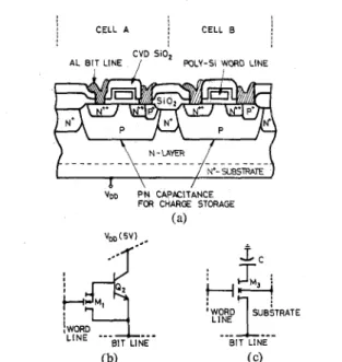
( a)
(b) ( c)
Fig. 1. (a) Cross-sectional views of two new dynamic RAM cells; equiv- alent circuit of (b) a new dynamic RAM cell; (c) a conventional
1 T cell.
11. CELL OPERATIONS
The basic integrated structure of the proposed new dynamic RAM cell is shown in Fig. l(a). This cell mainly contains an n-MOSFET siting on a p-well. The polysilicon gate is extended to form the word line while the aluminum line, which contacts one of the two n++ regions in the n-MOSFET, is extended to form the bit line. The other n++ region is connected to the p+ region of the p-well through an aluminum contact. Besides the n-MOSFET M I , there is a merged BJT Q 2 with the n-substrate as collector, p-well as base, and n+* bit line diffusion region as emitter. Thus the equivalent circuit of the new cell may be drawn as in Fig. l(b). As compared with the 1T cell circuit shown in Fig. I(c), the M I transistor in the new cell serves as a transfer gate to charge or discharge the storage capacitor, similar to the M 3 transistor in the 1T cell. However, the storage capacitor here is base-collector p-n junction capacitor which lies beneath the M I transistor, instead of an MOS capac- itor upon the semiconductor surface as in the case of 1T cell.
To write 1, the word line potential of the selected cell is rised from 0 to 5 V and its bit line potential is also rised to 5 V. At this time, the transistorMl is turned on and the p-well, Le., the base region of the transistor Q 2 , is charged. Then the bit line is left floating by a clock such as chip-enable clock. During this time, the word line potential is dropped to 0 V. At last the whole write 1 operation is finished by promoting the bit line potential to standby level VREF which is equal to VDD (5 V). If the charging action is complete, just after the write operation, the voltage at the base terminal called the storage node is
vSl = vDD
-
vth* (1)To write 0, the operation is similar to that of write 1 except that the bit line potential is lowered to 0 V. During the opera- tion, the storage node potential first is discharged to 0 V and
888 IEEE TRANSAI:'TIONS ON ELECTRON DEVICES, VOL. ED-30, NO. 8, AUGUST 1983 finally is rised to some positive level by the capacitance cou.
pling effect. Therefore, just after the write operation, tht: voltage level Vso may be expressed by
vso
=vco
( 2 1where Vc0 is the coupling voltage on the junction capacitanc,: CBC through CBE. Since CBC and CBE are all voltage depen" dent, Vco should be determined by the transient calculations.
To determine the final voltage at the storage node, the c e % after the write l(0) operation is considered to be always deselected before the next refresh cycle reaches. If this deselected cell is subjected to the standby operation, the bit line potential is kept at 5 V ( VREF) and two junctions of the bipolar transistor are reverse-biased. Thus the storage node I S isolated from the bit line except that small reverse saturation current and leakage current flow through both reverse-biaseS junctions. Although these currents tend to increase the poter.. tial of storage node, such increase is so small that the potenti;ll of storage node will be nearly undisturbed. In the read and the write binary 1 operations, bit line potential is either 5 or nelr
5 V. Thus the deselected cell is not severely disturbed as i n the standby case.
In the write or read binary 0 operation, the bit line potenti;ll
is lowered to 0 V. At this moment, the storage node of the deselected cell storing binary 0 is also lowered to a small positive residue voltage which is generated during the standby period by the charging of small currents in reverse biased jun ;- tions. As the bit line remains a t 0 V, the increasing rate of this residue voltage will be lower than that in the standby c a x because charging currents to the storage node from the two junctions are opposed rather than superposed. After the bit
line potential is rised back to 5 V, the storage node potentiil is also rised to that of binary 0 and the original stored data is restored without destruction.
For the deselected cell storing binary 1, the voltage o n t l e storage node is high. As the bit line potential is decreased lo
0 V in the write or read binary 0 operation, the storage notle voltage is decreased according to the capacitance coupling effect between base-collectorjunction capacitance and emitter- base junction capacitance. Finally, the emitter-base junction i.s
forward-biased while the base-collector junction is kept reverse- biased. At this moment, the transient base-emitter volta1:e V B ~ , which is determined by the base-collector and base- emitter junction capacitances during .the transient procels, tends to be decreased by the base-emitter discharging currer!i. This current is formed by the net flow of: 1) holes injected fro) m
base to emitter; 2 ) electrons injected from emitter and not col- lected by the collector and 3) holes injected from collector :o
base. The first two components are just the base current under VBET whereas the last component is approximately the reverse saturation current IC, of the base-collector junction. Thus tlre change of VB,, during the time period A t can be written as
A vBET = (IC0
-
Ic/O)At/(cBEJ f CB)v T A t ( r C O / T ~ I ~ - 1 / p T ~ ) 1)
where the forward base-emitter junction capacitance is the sum of base-charging capacitance CB = TFgm which is the dominant component, and the forward depletion capacitance CBEJ.
Assume that the deselected cell storing binary 1 is continu- ously subjected to the write or read binary 0 operation, the worst-case storage node voltage can be expressed as
b 1 , m i n = V B E ~ + VCI (4)
where VBEf is the final base-emitter voltage when the bit line voltage is 0 V, and
Vc1
is the coupling voltage. Note that V C ~ is greater than Vco since the initial condition for Vcl has a larger forward-biased emitter-base junction capacitanceCBE.
From the above considerations, it is seen that if A VBE, is negligibly small, both VBEF and V ~ l , ~ h will be nearly the same as those in t h e f i s t time the bit line voltage is 0 V, and the stored voltage will be not severely distributed. However, if A V B ~ r is large, V B E ~ will be equal to the steady-state open- base base-emitter voltage, and the binary 1 will be held with a lower V S I , ~ ~ .
In the case of very large CBc/CBE ratio, both VC, and VCO are small. Thus VSo 0, Vsl,mh V B E ~ , and the stored in- formations will still be not destroyed. It should be emphasized that only when the storage node voltage of the deselected cell storing binary 0 has enough long time to be charged to V B E ~ the stored information could be destroyed.
In the proposed cell structure, both the emitter and base impurity concentration difference and the base width, i.e., the difference of p-well depth and source/drain depth, is
rather large. This leads to a large
PTF.
Furthermore, the time period At in the write or rewrite binary 0 operation can be small as will be seen in Section IV. Thus A VBET can be strictly reduced. With very small A VBE,, each time the stored binary1 level in the deselected cell storing binary 1 is recovered from one write or read binary 0 operation, the loss of its storage node voltage is quite small.
When the cell is scaled down, the base area is reduced and a smaller CBc is resulted. The base-emitter C B ~ is, however, also reduced to obtain the same or larger CBC/CBE ratio. Moreover, in the scaled-down cell, both the depth and the im- purity concentration of the sourcejdrain and the p-well can be designed to obtain the same large
PTF
and the smaller At. Thus very small AV,,, can also be obtained. Under this case, the stored binary 1 in the deselected cell is still not distroyed.From ( 2 ) and (4), the stored charge quantity on the storage capacitor of the cell is written as
Q i l = C B C ( ~ D D - Vs/sl,min)=CBC(VDD - VBEf- Vc1) ( 5 )
Qto = CBC( ~ D D
- VSO)
(6)where Q i l
(eio)
is the charge quantity when the cell storesl(0). Therefore the signal swing on the bit line with capaci- tance CBL is
WU: DRAM CELL IJSING BWPOLAR-MOS COMPOSITE STRUCTURE 889
The bit line capacitance per cell generally contains three components: 1) CBE in series with CBC; 2 ) gate-source overlap capacitance C,, which is much smaller than that in l), and 3) parasitic capacitance Cp which is also much smaller than that in 1). For a bit line with n cells connected in it, CBL may be written as
Substituting (8) in (7), we have
1
From (9), it is seen that the signal size is strongly dependent upon the capacitance ratio CBEICBC. As the bit capacity in- creases, n increases and CBE/CBC should be decreased in order to ob.tain a detectable VI" The decrease ofjunction capacitance ratio CBE/CBC can be achieved by increasing CBC and/or decre;asing CBE which are all feasible through various process technologies.
111. PERFORMANCE A . Chip Area
Since every cell has its own p-well as shown in Fig. 1, the spacing between two p-wells is the most important parameter in determining the cell area. Fortunately, the spacing can be strict:ly minimized due to the following reasons:
a) Only n-regions are connected to the power supply or the bit line while all p-regions are left floating. There is n o way for the hold current to flow. Thuslatchup cannot occur among the cr:lls.
b) The n+ region between two p-wells, which is formed be- fore p-well implantation has a higher impurity concentration than the p-well region. Thus the lateral diffusion of p-well and the space charge width in n+ region are effectively reduced.
c) The vertical scale down of p-well [8] also reduces the spacing between p-wells.
Although an extra contact is needed, the area of this contact plus 'other spacings is expected to be smaller than that of capac- itor .in conventional 1T cell. Thus the total chip area of the new cell will be smaller. Based on the single-poly process technology with minimum feature F and the same design rule in the BO-MOS cell [7]
,
the minimum cell area is 14.875F2 as indicated in the layout shown in Fig. 2. For F = 3 Bm, the area is 134 pm2 which is smaller than that of 1T cell and VMOS cell, comparable with that of Hi-C cell [ l ] and PTI cell, but larger than that of a BO-MOS cell.B. Storage Capacitance
In general the p-n junction reverse-bias capacitance per unit area is lower than the MOS capacitance per unit area. This disadvantage can be compensated partially by the fact that the, entire cell area is available for the p-well which forms the cell storage capacitor with the n-substrate, and the fact that the
depth of p-well is large to provide considerable sidewall capacitance. Moreover the n+ diffwion on the n-substrate
between p-wells is effective to increase the sidewall capacitance. According to the cell layout in Fig. 2 , the bottom area of p-well is 7 times that of n++ region whereas the typical depth of p-well is nearly 4 times that of nt+ region. Furthermore, the difference between doping concentrations of two p-n junction capacitance CBc and CBE is offset by the n" diffusion on the substrate. Therefore the ratio CBC/C'E can be made large to obtain a larger signal size.
C.
Leakage ConsiderationsThe leakage current of a reverse-biased p-n junction generally increases with the junction area and decreases with the impu- rity concentration. Therefore the storage capacitance CBc has a larger current than the bit line capacitance CBE when the cell is in its standby mode. However, these two currents are ex- pected to be low even at high bias because the p-well doping is quite low to effectively reduce tunneling [9] in both reverse- biased junctions despite of the high doping concentration of both n+ and n++ regions.
The n+ region between p-wells is effective to decrease the numbers of hole-electron pairs generated in the depletion region by a-particles or cosmic rays [ l o ] and to repel the migrating holes from the bulk [ 7 ] . Therefore the soft-error immunity is not worse than the conventional 1 T cell. D. Process Compatibilities
As may be seen from the integrated structure of the new cell shown in Fig. l(a), the fabrication process is similar to that of Si-gate p-well CMOS except an extra n+ implantation. Thus the cell can be easily fabricated by using the conventional technologies without paying a lot of efforts to develope other complicate or difficult processes. Moreover, the peripheral circuits can be built with CMOS, the way leading to a simpler
890 IEEE TRANE/"rCTIONS ON ELECTRON DEVICES, VOL. ED-30, NO. 8, AUGUST 1983 TABLE I
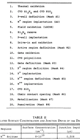
TYPICAL FABRICATION PROCESSES OF THE NEW CELL 1. 2. 3. 4 . 5. 6 . 7. 8. 9 . 1 0 . 11. 1 2 . 13. 1 4 . 15. 1 6 . 1 7 . 18. 1 9 . 20. Thermal o x i d a t i o n CVD Si3N4 and CVD S i 0 2 P - w e l l d e f i n i t i o n (Mask #1) N+ r e g i o n i m p l a n t a t i o n ( A S ) F i e l d o x i d a t i o n (LOCOS) S i N remove P - w e l l i m p l a n t a t i o n D r i v e - i n a n d o x i d a t i o n A c t i v e r e g i o n d e f i n i t i o n (Mask # 2 ) Gate o x i d a t i o n CVD p o l y s i l i c o n G a t e d e f i n i t i o n (Mask # 3 ) P+ r e g i o n d e f i n i t i o n (Mask # 4 ) P+ i m p l a n t a t i o n N++ r e g i o n d e f i n i t i o n (Mask 15) N++ i m p l a n t a t i o n CVD S i 0 2 Ohmic c o n t a c t o p e n i n g (Mask X6) M e t a l l i z a t i o n (Mask #7) P a s s i v a t i o n (Mask 1 8 ) 3 4 TABLE I1
S I M U L A T E D S U R F A C E C O N C E N T R A T I O N A N D JUNCTION DEPTH O F T H E DEVU: Z
Regions N++ E m i t t e r a x 1 0 1 9 0.508 S u r f a c e C o n c e n t r a t i o n J u n c t i o n Depth (cm-3) (vm) N + D i f f u s i o n 2 . 6 9 0 5x1oI6 P-Well 1.540 5 x 1 0 ~ ' N-Layer
I
5 x 1 0 ~ ~I
-
circuit design [ I 11 and a better balance of power and speed To be compatible with the n-well CMOS technology, the proposed cell can also be made on p-substrate with an n-well ;is
its storage node and an p+ region as its emitter. [I21
IV. SIMULATED RESULTS
The proposed fabrication processes of the new cell with a p-type well are listed in Table I where only main steps are concerned. Except the n+ region implantation which may als 2
be viewed as a kind of field implantation, the processes are juzt the same as those of a typical p-well Si-gate CMOS. Based 0.1 the actual process parameters, the simulated surface concentrz
-
tions and junction depths of the cell, which are generated frorl the SUPREM program [13], are shown in Table 11.
To calculate the reversed junction capacitance, all the im- planted profiles are assumed to be of Gaussian distributio~r which is a good approximation to the simulated profiles ill.
- .
1
---
BIT LINE-
x x a STORAGE NODE -1.01 0' 10 x) 30 40 V," 50 =, 1 v 60 , 70 El 90 100 XTj TIME (NSEC)Fig. 3. Simulated timing diagram of the write operation.
TABLE I11
P R O P O S E D DEVICE D I M E N S I O N IN THE SCALED-DOWK C E L L
P-well Depth (urn)
Source-Drain Depth I p m ) 0.1
N+ Depth ( P m ) 0.5
Surface Concentrations A l l Unchanged
TABLE IV
CALCULATED JUNCTION C A P A C I T A N C E S A N D T H E I R R A T I O S A T
DIFFERENT M I N I M U M FEATURE S I Z E
Fig. 3. The capacitance of the bottom plate in B-E and B-C junctions is calculated by the method proposed by Lin [14].
The sidewall capacitance of the p-well touching the n-region is calculated by the conventional method [ 151 whereas the side- wall capacitance of the p-well touching the n+ region and the sidewall capacitance of B-E junction, both being of double Gaussian distribution, are calculated by the numerical method [16]. Based on these methods, a simulation program for the reversed junction capacitance has been constructed to simulate the cell capacitances.
According to the cell layout shown in Fig. 2 and the simu- lated profiles, a scale-down on the dimension of the cell is proposed, as shown in Table 111, to investigate the performance of the scaled-down cell. Both the p-well and the source-drain junction depths are not subjected to scale down until the mini- mum feature size is below 3 pm. The surface impurity concen- trations of all the implantation regions remain the same as those in Table I for all values of F .
The total capacitance ratio CBc to C,, and, their sidewall capacitance ratio for the cells storing binary 1 are listed in Table IV. For the cell with the n+ diffusion outside the p-well
WU: DRAM CELL USING BIPOLAR-MOS COMPOSITE STRUCTURE 891
the ratio increases from 3.8 at F = 5 pm to 5.2 at F = 3 pm and finally to 14.8 at F = 0.5 pm. This implies that when the cell area .is scaled down in order to be used in a larger RAM, the ratio of storage capacitance t o bit line capacitance is favorably increased without invohing critical processes such as thin capacitor oxide growth as the conventional 1T cell should do. This increase is due to th.e following reasons:
a) Due to the logarithmic dependence of the sidewall capac- itance per unit area on the depletion width [ 151 , the difference of the sidewall capacitance density between B-C and B-E junc- tions is smaller than that of the bottom plate capacitance density. Therefore the total sidewall capacitance in the B-C junction which has a larger sidewall area, is larger than in the B-E junction and their ratio is large as may be seen from Table IV. When the horizontal dimension is scaled down by a factor K and the vertical dimension remains unchanged, the sidewall area and its capacitance become more and more significant. Theriefore, although the sidewall capacitance ratio is not changed, the total capacitance ratio is still increased from F = 5 pm to F == 3 pm as listed in Table IV. The increase of sidewall capacitance ratio when F is smaller then 3 p m is due to th.e increase in the percentage of p-well sidewall area touch- ing the n+ region. This increase also contributes part of the increase of the ratio
CB~-/CBE.
b) The p-well depth is scaled down under the fixed surface impurity concentration. This leads to a lower p-well concentra- tion at the B-E junction and a larger gradient at the B-C junc- tion. Therefore when scaled down,
CBE
is decreased more fast .than CBc is, as listed in Table IV. This leads to the result that the ratioCBC/CBE
is remarkably increased from F = 2 pm to F = 0.5 pm as listed in Table IV.For the purpose of comparison, the ratios and capacitances for the cell without the n+ diffusion are also listed in Table IV. The increase of CBC by the n+ diffusion can be easily seen. For the cell storing binary 0, the characteristics are similar to those of the cell storing binary 1 cited earlier.
To show the dynamic characteristics of the cell, the voltages of V&,, VB,, Vel, and
VCO
are simulated by using the SPICE program [17] and are listed in Table V for differentCBCICBE.
In this table, the value of
VBE,
is determined at the first time the bit line is lowered to 0 V just after 'the write 1 operation, that of V S ~(VS,) is determined from the worst case that , ~ ~ the bit line voltage has been kept at 0 V ( 5 V) 2 ms long. Based on these data, the number of cells n which can be con- nected together on one bit line and can offer 100-mV signal size in the worst case, is estimated by (9) and is also listed in Table V. It may be seen that at larger value ofCBC/CBE,
the signal swing V S ~- VSO , ~is smaller than the value of ~ V D D-
Vth. Therefore the value of n is smaller than the 1T cell for the same bit line capacitance to storage capacitance ratio. However, theCBC/CBE
ratio is large when the cell is scaled down. This leads to a large enough n value to be used in a large DRAM.Typical write transient waveforms in the case of large (= 10)
CBC/CBE ratio which is the practical condition for DRAM cells, are shown in Fig. 3. It is evident that V S ~N V B ~ f , ~ and ~
YSO
2: 0 as predicted in Section 11.TABLE V
C A L C U L A T E D V O L T A G E LEVELS AND N U M B E R OF C E L L S PER BIT LINE FOR
100-mV SIGSAL SIZE IN THE CELLS WITH DIFFERENT CBC/ CBE 8 = 2 5 0 T =0.7ns Device Parameters F VTh'l. ov c,,=0,016pf (-4V bias) VRFIT ( v )
I
0 . 4 5 4 7I
0 . 4 4 2 6 1 0 . 4 2 8 7 1 0 . 1 8 5 0 'Sl,rnin (" vso (VI 0 . 7 3 0 . 3 9 1 . 7 5 2 . 3 7 0 . 7 3 3 . 0 3 2 . 2 1 1 . 0 9 number of cellsI
1 5 01
80.6I
3 61
28 ( W CELLSlBlT LINE) 0 0 0 BIT UNE (0) A A A BIT LINE ( 1 ) -WORD LINE TIME (NSEC)Fig, 4. Simulated timing diagram of the read operation.
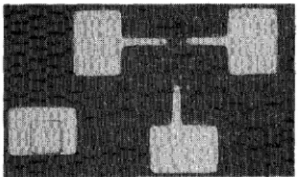
Fig. 5. Surface photograph of a fabricated cell.
The corresponding read transient is shown in Fig. 4 where the bit line capacitance CBL is 1 PF which is equivalent to that of bit line with 6 4 cells on it. The signal swing of 1 12 mV can be obtained within 10 ns.
V. EXPERIMENTAL RESULTS
To observe some properties of the proposed new dynamic RAM cell, a test chip for the new cell is designed by using 10-pm design rule. The fabrication processes are the same as listed in Table I except that the n+ diffusion region outside the p-well is simply defined by an extra mask rather than by the LOCOS method. The surface photograph of the fabricated cell is shown in Fig. 5 . The measured capacitance at various
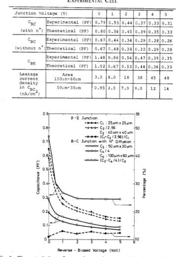
TABLE VI
JUKCTION CAPACITANCE AND LEAKAGE CURRENT DENSITY O F THE
EXPERIMEUTAL CELL I 0 9 55 B - E Junctton --M- CT .25um x 25um C2 . 4 0 u m x 4 0 ~ l m 8 - C Junctlon
-
w t h N' D l f f u s i m CJ : 50umx30urn - c * / 4 -.e+ (C,-C2 I 2 . % ) I C ,Reverse - Bfased Voltage (Volt)
Fig. 6 . Characteristics of capacitance increment in the scaled-dow a B-C and B-E junctions.
reverse-biased voltages for the base-collector junction wit.l and without n+ diffusion and the base-emitter junction are listed in Table VI. As may be seen from Table VI, the capac .
itance is increased by the n+ diffusion. However, since th.s fabricated cell is not optimized in its dimension, the capac .I
tance CBE appears larger than CBC. Theoretical calculatiorrs are also compared to the experimental results and a satisfactor:/ agreement between them is obtained.
To investigate the scale-down properties of the cell capaci. tances, the capacitances of two B-C junctions with an are,] ratio 4 and two B-E junctions with an area ratio 2.56 are mea- sured and the results are shown in Fig. 6. Due to the contri- bution of the sidewall capacitance as mentioned in Section IV, the capacitance of the scaled-down B-C junction is larger tharl one-fourth of the capacitance of the larger B-C junction b:!r 24 percent. It is larger than that of B-E junction, 1 2 percent. Therefore the scale-down is effective to increase the ratio
Typical leakage current density of two B-C junctions a : various reverse voltages is listed in Table VI where the increasc of current with respect to the increase of voltage is rathe. small. Therefore the tunneling current component 191 in thes(: junctions is negligible. CBClcBE * - 2 v Reverse B ~ o s - 4 V Reverse BIOS - 2 V Rwerse Bias B - C Junction wtth N' Diffusion I C 4 V Reverse 810s -2V Reverse Bias - 4 V Reverse Bias 8 - E Junctlon Temperature ( T )
Fig. 7. Leakage current as a function of ambient temperature in various p-n junctions.
Since the leakage current in the sidewall junction which has higher impurity concentration is smaller than that in the bottom junction and the contribution of sidewall become more signifi- cant than that of bottom wall when scaled down. Thus the total leakage current density of the whole junction is smaller in the smaller junction than in the larger one as listed in Table VI. Similar result is also obtained in the case of B-E junction.
When the reverse-biased junction voltage exceeds 1 V, the variation of capacitance with temperature in both junctions are observed to be negligibly small. However the leakage cur- rent is increased with the increase of ambient temperature as shown in Fig. 7 where the B-E junction, the B-C junction with n+ diffusion, and the B-C junction without n+ diffusion are measured. It may be seen that the n+ diffusion in the sidewall
is also effective in reducing leakage current. From Fig. 7, the total leakage current I, of the cell storing binary 0 is about 1.25 pA at 25°C. For the averaged storage capacitance C ~ C =
0.44 pF and voltage swing between 0 and 1 A V = 1 V, the storage time t, of the fabricated cell may be estimated by [7]
ts = C,
A
V/IL = 350 ms.When the cell is operated at 1 20"C, the storage time reduces to 6 ms due to a larger I, = 73 PA.
Dynamic test of the fabricated cell is also performed. The waveforms in the write 1 and standby operations are shown in Fig. 8(a) with test circuit shown in Fig. 8(b). The cell is first selected to write 1 and then is deselected. During the dese- lected or standby period, the bit line voltage is subjected to several times of droping to 0 V. However, the storage node voltage can follow the bit line voltage changes and recover itself without destroying the stored binary 1. Note that short
WU: DRAM CELL USING BIPOLAR-MOS COMPOSITE STRUCTURE
Fig. 8. (a) Dynamic waveforms of the write 1 and standby operations; (b) its test circuit.
(b)
Fig. 9. (a) Dynamic waveforms of the write 0 and standby operations; (b) its test circuit.
clocks are used to prevent the cell from discharging through the input resistance of the probe. Thus the storage node volt- age can be directly observed.
The waveforrns in the write 0 and standby operations are shown in Fig. 9(a) with the test circuit shown in Fig. 9(b). The cell is first selected to write 1 and then write 0, finally is deselected and standby at binary 0. The voltage difference of the storage node between 0 and 1 is clearly seen. Due to
893
the effect of the external circuit the charging of write 1 is slow down in this test.
VI. DISCUSSION AND CONCLUSION
We have proposed a new dynamic RAM cell which consists of an n-channel MOSFET as a transfer gate and a base-collector junction of a merged BJT as a storage capacitor. The write and read operations of the new cell have been analyzed, described, and simulated. It has been shown that the signal size depends upon the capacitance ratio of the base-collector junction and the base-emitter junction. In the standby operation, the cell leakage current is small enough to obtain a good data retention capability. The stored data in the deselected cell is not de- stroyed by the bit line potential variations.
Due to the facts that latchup cannot occur and lateral dif- fusion width is reduced by the n+ diffusion, the spacing between p-wells can be strictly minimized. Thus a minimum area 14.875F2 with a minimum feature size F is realizable. Furthermore, the n+ region between p-wells is effective to reduce carrier generation and collection, therefore the soft- error immunity of the cell is not worse than the conventional
1T cell.
Unlike other cells using the buried junction storage, no epi- taxy or I/-groove cutting is required. The fabrication technol- ogy of the cell is fully compatible with that of p-well or n-well Si-gate CMOS. Using the p-well silicon-gate CMOS processes and relaxed design rule, the experimental cell is fabricated and tested. The fabricated cell has a leakage current of 1.25 pA at 25°C and an averaged storage capacitance of 0.44 pF, which lead to a storage time of 350 ms. Dynamic test of the fabri- cated cell is also successfully performed to verify the cell operation descriptions. However, because optimal dimension
is not performed in the fabricated cell, the capacitance ratio is small. Further improvements on the cell will be done and a whole test RAM IC will be fabricated in the near future.
When the cell is scaled down, the capacitance ratio is simu- lated to be increased from 3.8 at F = 5 pm to 5.2 at F = 3 pm and finally to 14.8 at F = 0.5 pm, This is due to the contribu- tions of both the sidewall junction and the p-well doping profile. The number of cell per bit line for 100-mV signal size is also increased as the cell is scaled down. Furthermore the leakage current density is reduced when scaled down.
In summary, the proposed new cell has simple fabrication process and good performance of large storage capacitance to bit-line capacitance ratio, as well as fairly good packing density, soft-error immunity and leakage characteris.tics. Moreover, as compared with the conventional 1T cell, the scaling down of the cell can be performed with less processing troubles and better performance can be obtained. Thus it is felt that the new cell has great potential for further developments.
ACKNOWLEDGMENT
The author wishes to thank D. J. Neiu, M. Z. Lin, and the
Technical Staff of Semiconductor Research Center, National Chiao Tung University for the fabrication of the devices. Valuable suggestions by the reviewers are greatfully acknowl- edged.
a94 IEEE TRANSti.::TIONS ON ELECTRON DEVICES, VOL. ED-30, NO. 8 , AUGUST 1983
REFERENCES
[ l ] P. K. Chatterjee, G. W. Taylor, R. L. Easley, H. S. Fu, and A. F
Tasch, Jr., “A survey of high-density dynamic RAM cell c o n cepts,” IEEE Trans. Electron Devices, vol. ED-26, pp. 827-8391, June 1979.
[2] R. H. Dennard, “Field-effect transistor memory,’’ U.S. Paten: 3 387 286, June 4, 1968.
[3] V. L. Rideout, “One-device cells for dynamic random-acces;; memories: A tutoria1,”ZEEE Trans. Electron Devices, vol. ED-26 pp. 839-852, June 1979.
[4] P. K. Chatterjee, G. W. Taylor, A. F. Tasch, Jr., and H. S. Fu “Leakage studies in high-density dynamic MOS memory devices,’ ZEEE Trans. Electron Devices, vol. ED-26, pp. 564-576, A ~ I
1979.
[SI J. J. Barnes, S. N. Shodle, and F. B. Jenne, “The buried-sourcc V-MOS dynamic RAM device,” inZEDM Tech. Dig., p. 272, 1978. [6] G. W. Taylor, P. K. Chatterjee, H. S. Fu, and A. F. Tasch, Jr. “A punch-through isolated RAM cell,” in ZEDM Tech. Dig. p. 352, 1978.
[7] J. Sakurai, “An experimental study of the BO-MOS dvnamil: RAM cell,” IEEE Tian. Electron Devices, vol. ED-28, pp: 1178- 1182, Oct. 1981.
[ 8 ] R. D: Rung, C. J. Dell’oca, and L. G. Walker, “A retrograde
p-well for higher density CMOS,” ZEEE Trans. Electron Devices, I. Antipov, !‘Proposed process modifications for dynamic bipolar memory to reduce emitter-base leakage current,” ZEEE J. Solid- State Circuits, vol. SC-15, pp. 714-719, Aug. 1980.
C. Cohen, “DO cosmic rays spell death for VLSI?” Electron., R. Bernhard, “The 64-Kb RAM teaches a VLSI lesson,” ZEEE Spectrum, pp. 38-42, June 1981.
W. R. Iversen, “CMOS promises huge dynamic RAMS,” Electron., D. A. Antoniadis, S. E. Hansen, and R. W. Dutton, Stanford University, Stanford, CA, Tech. Rept. 5019-2.
H. C. Lin, “Depletion-layer calculations of a doublediffused junction,” ZEEE Trans. Electron Devices, vol. ED-27, pp. 1839-
1841, Sept. 1980.
S. M. Sze, Physics of SemiconductorDevices. New York: Wiley, 1969, ch. 3, p. 91.
A. B. Bhattacharyya and T. N. Basavaraj, “Transition-capacitance calculations for double-diffused p n junctions,” Solid-state Electron., vol. 16, pp. 467-476, 1973.
A. Vladimirescu, A. R. Newton, and D. 0. Pederson, SPICE
Version 2G.1 User’s Guide, Dept. Elec. Eng. and Comput. Sci., University California, Berkeley, CA, Oct. 1980.
V O ~ . ED-28, pp. 1115-1119, Oct. 1981.
pp. 44-46, NOV. 22,1979.
pp. 75-78, Oct. 6 , 1981.
Silicon-Rich Si02 and Thermal Si02 Dual Dielectric
for Yield Improvemenmt and High Capacitance
STEFAN K.-C. LAI, D. J. DIMARIA, A N 3 FRANK F. FANG, SENIOR MEMBER, IEEE
Abstract-The use of silicon-rich Si02 and thermalSiO2 dual dielectric in memory capacitors and FET’s is investigated. It is shown that thc silicon-rich layer was conductive and introduced only a small decreasc: in the series capacitance of the dual dielectric. Consequently, the capac itance of the dual dielectric is close to that of the thermal oxide only,
The response time of the silicon-rich layer is measured by using FE’I response time and is shown to be in the nanosecond range. With thi;! fast response time, it is possible to use the dual dielectric in memoq, and logic circuits. Another advantage of the dual dielectric is the ver!, high yield due to the field screening of the silicon-rich layer to an) nonuniformities in the thermal oxide or at the SiOz-contact interface This dual dielectric has the promise of high yield and high capacitancc for future VLSI circuits.
I
I. INTRODUCTION .
N VLSI circuits, a high-dielectric-constant gate-material is very desirable. It can increase storage capacitance in 1-
Manuscript received December 24, 1982; revised March 14, 1983 This work was sponsored by the Defense Advance Research Project! Agency (DoD) ARPA order number 4012 under Contract MDA903-81’ C-0100 issued by the Department of Army, Defense Supply Service Washington, DC.
S. K.-C. Lai was with IBM Thomas J. Watson Research Center, York town Hekhts. NY 10598. He is now with Intel Corporation, Sant;i Clara, CA% OS 1.
Center, Yorktown Heights, NY 10598.
D. J. DiMaria and F. F. Fang are with IBM Thomas J. Watson Researct
device dynamic memory cells [ 1 ] thus increasing signal levels and reducing the impact of alpha particles [ 2 ] , increasing transconductance of FET’s, and reducing short-channel effects
[ 3 ] . Insulators like silicon nitride [4] and tantalum pentoxide [ 5 ] have been proposed and used to give higher dielectric constant compared to that of thermal oxide. However, the use of such insulators is still experimental, and their compati- bility with standard polysilicon gate processing and long-term reliability are questionable.
Recently, it was demonstrated that silicon-rich silicon dioxide (deposited by CVD with approximately 13-percent excess silicon) [6] could be used on top of thermal silicon dioxide for enhanced electron injection into the oxide [7] - [ 9 ] . Further- more, silicon-rich oxide has a high dielectric constant (approxi- mately 7.5 in the above composition) and such a composite structure has been demonstrated to have well controlled high field conduction properties [9]