國 立 交 通 大 學
電子物理研究所
碩 士 論 文
氮化銦磊晶層之快速熱退火效應
Effect of rapid thermal annealing on
InN epilayers
研 究 生:李啟仁
指導教授:周武清教授
氮化銦磊晶層之快速熱退火效應
Effect of rapid thermal annealing on
InN epilayers
研 究 生:李啟仁 Student:Chi-Jen Li
指導教授:周武清教授 Advisor:Prof. Wu-Ching Chou
國 立 交 通 大 學
電子物理研究所
碩 士 論 文
A Thesis Submitted to Institute of Electrophysics College of ScienceNational Chiao Tung University in partial Fulfillment of the Requirements
for the Degree of Master in Electrophysics July 2006 Hsinchu, Taiwan, Republic of China
氮化銦磊晶層之快速熱退火效應
研究生:李啟仁 指導教授:周武清博士國立交通大學電子物理研究所
中文摘要
在本論文中,我們利用了光激螢光光譜與吸收光譜來研究氮化 銦磊晶層的光學特性,並且研究快速熱退火對氮化銦磊晶層物性的 影響。當氮化銦磊晶層載子濃度增加時,光激螢光光譜與吸收光譜 位置會往高能量移動,此種現象為典型的 Burstein-Moss 位移。此 外氮化銦磊晶層光激螢光光譜其包含了電子分別與深層和淺層授 子的複合放射,因此其波形是呈現高度不對稱的現象。此外從亞倫 尼斯圖法可以獲得兩個活化能,其分別代表深層授子的束縛能(50 ~55 毫電子伏特)與淺層授子的束縛能(5~10 毫電子伏特)。 此外氮化銦磊晶層經由快速熱退火處理後,隨著退火的溫度的 增加其光激螢光光譜半高寬降低、波形從不對稱趨於對稱、譜峰位 置往低能量位移與積分強度增加。其中半高寬的降低與波形趨於對 稱的原因為深層能階有效的經由退火處理而被抑制。此外從霍爾量 測可以得知快速熱退火可有效的降低氮化銦磊晶層之載子濃度。Effect of rapid thermal annealing on
InN epilayers
Student:Chi-Jen Li Advisor:Dr. Wu-Ching Chou
Institute of Electrophysics National Chiao Tung University
Abstract
In this thesis, micro-photoluminescense (μ-PL) and absorption were employed to investigate the optical properties of InN epilayers. The effect of rapid thermal annealing on the physical properties of InN epilayer was also studied. The PL and absorption edge of InN epilayers blueshift due to the Burstein-Moss effect when the carrier concentration increases. The photoluminescence lineshape of InN epilayer were highly asymmetry because the photoluminescence origin involved the electron to the deep and shallow acceptor transition. In addition, temperature dependence of the integrated PL intensity of InN epilayers was investigated. Two activation energies were obtained from the Arrhenius plot. We ascribe them to the binding energy of deep acceptor (Eda) (50~55 meV) and
shallow acceptor (Esh) (5~10 meV), respectively.
We also found that the rapid thermal annealing significantly decreases the carrier concentration of InN epilayers as well as the full width at half
maximum (FWHM) of PL bands. Besides, the integrated PL intensity also increases by the RTA treatment. In our typical PL spectra, highly asymmetric line shape was observed. The emission line-shape became symmetric after the annealing treatment because the deep acceptor transition was suppressed.
致謝
終於完成碩士兩年學習生涯,雖然辛苦但也讓我學習到很多實驗 技巧和待人處世的態度,內心除了充滿著欣喜,也充滿了感激。感謝 周武清、李明知、陳衛國及張文豪老師的細心指導,給予我協助與鼓 勵。特別要感謝指導教授周武清老師不厭其煩的諄諄教誨,讓我可以 順利的完成論文研究。另外,要感謝古慶順、柯文政、李寧、陳京玉、 傅振邦、蔡文哲等學長的指導。特別要感謝傅振邦學長在我實驗的過 程當中分享經驗及建議,讓我少走了很多冤枉路。感謝蔡文哲學長在 我實驗遇到問題時常常陪我熬夜及陪我討論,讓我倍感窩心。更要謝 謝同學維偲、尚樺、士傑、泰鑫、士凱在這段日子的陪伴與照顧,還 有學弟妹少甫、沛雯、家禎、進吉、書鴻、仲葳、峰毅帶給我們歡笑, 讓我留下很多美好的回憶。 最後,要特別感謝的是我的父母及家人,因為有你們的幫忙及精 神上的支持,讓我可以無憂無慮的完成我的碩士生涯,謝謝你們! 啟仁 於新竹交大 95.7
Index
Abstract (Chinese version) ……….... i
Abstract (English version) ……….…ii
Acknowledgment………....iv
Index………....v
Chapter 1 Introduction ……… ….….1
Chapter 2 Theoretical background for photoluminescence in semiconductors ………...3
Chapter 3 Experiments ………...7
3.1 Sample preparations ………...7
3.2 Measurement techniques ………..11
Chapter 4 Results and discussion ………..15
4.1 Emission and absorption properties of InN epilayers……....15
4.2 Rapid thermal annealing of InN epilayers ………19
Chapter 5 Conclusions ………...30
Chapter 1 Introduction
InN is the least studied material of III-nitride, which is currently attracting intense interests. The band gap of wurtzite InN was believed to be about 1.9~2.0 eV in the early years [1]. But in recent reports, the controversy of InN band gap was resolved and was accepted to be about 0.7 eV [2-4]. The discrepancy in the InN band gap might be attributed to the strong Burstein-Moss effect due to the high unintentional doping concentration [5,14]. The sources of the high density of background carrier concentration commonly observed for this material is also unconfirmed. Several suggestions of high carrier concentration sources for InN grown by different growth techniques are: (i) oxygen atoms on nitrogen site [6]; (ii) hydrogen incorporation [7]; (iii) nitrogen vacancies [8]; (iv) nitrogen anti-site [9]. Compared with AlN and GaN, it is more difficult to grow high-quality InN films due to the low dissociation temperature and the extremely high vapor pressure of nitrogen for InN. Efforts were devoted to improve the growth techniques in order to have better quality of InN. InN epilayers of better crystal quality with carrier concentrations below 1017~1018 cm-3 and mobility of about 2100 cm2/Vs were produced [10,11]. Thermal annealing was also employed to further improve the crystal quality [10,12].
Photoluminescence (PL) experiment is usually used to evaluate the crystal quality and investigate the nature of the recombination processes. Recent studies of InN showed that the PL spectrum exhibits one broad band with a highly asymmetric line-shape. The asymmetric line-shape is
ascribed to the emission of two recombination processes. One is related to the transition of degenerate electrons to the shallow acceptors with the binding energy of 5 ~ 10 meV and the other is attributed to the recombination of degenerate electrons with the holes trapped by deep acceptors with binding energy of 50 ~ 55 meV [13]. These experimental data and model calculation provide us a deeper understanding of physical properties of this material.
However, the investigation of sources of deep acceptor and shallow acceptor on InN epilayers is still lack. Thus, in order to understand the role of deep acceptor and shallow acceptor. The study of the effect of rapid thermal annealing on the physical properties of InN could give us another aspect of view to realize the influence of deep acceptor and shallow acceptor.
There are five chapters in this thesis. Theoretical back ground is briefly described in chapter 2. The experiment setups of photoluminescence and sample preparations as well as operation procedures of rapid thermal annealing (RTA) are presented in chapter 3. In chapter 4, we discuss the results of low-temperature and temperature-dependence micro-PL spectra of the RTA InN epilayers. Finally, we summarize the experimental results in Chapter 5.
Capter 2 Theoretical background
When the incident photon energy is larger than the semiconductor band gap, the electrons can be excited from the valence band to conduction band. The photon was emitted when an electron in an excited state drops down into an empty state in the lower energy state. For this to be possible, we must first inject electrons, which then relax to the state where the emission occurs. This could be the bottom of the conduction band, but is might also be a discrete level. If the defect or impurities exist in the semiconductor, the electron-hole pairs may be attracted by them to produce defect bound excitons. However there are also non-radiative recombination paths that do not emit photons so that the emission efficiency will be reduced. The fundamental radiative transitions and non-radiative recombinations are described as follows:
(A) Radiative transtion
(Ι) band to band transition
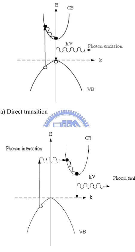
Band-to-band transitions involving free electrons and holes. Such transitions usually occur in direct-bandgap materials, such as III-V compounds, between C- and V-bands with conservation of momentum. The e-h pairs will recombine radiatively with a high probability. As shown in Fig. 2-1.
The total e-h recombination rate is given by R=
∫
R(hν)d(hν)≈npWhere n, p is the electron and hole concentration respectively, h is Plank,
s constant, ν is the frequency of emitted photon. It is the higher free carrier, the higher recombination.
(II) Donor acceptor pair recombination (DAP)
Transition between donors and acceptors level. The electrons and holes can be created at the D+ and A-
site to produce neutral Do
and A0
centers. In returning to equilibrium, some of the electrons on the neutral donors will recombine radiatively with holes on the neutral acceptors. It can be represented by the reaction,
Do +Ao
→ hν+D+
+A-
It can emit photon with an energy as described by the following formula: DAP A D g DAP R e E E E h E × + + − = = ε ν ( ) 2
Where ED and EA are the binding energies of donor and acceptor,
repectively, e the charge, ε the dielectric constant of the material, and RDA
the donor-acceptor separation. (III) Exciton transition
The Coulomb interaction between the conduction band electrons and the valence band holes will result in the formation of the bound electron-hole pairs, that is called “ exciton ”. The exciton is analogous to “positron atom” – electron bound to a positron, and this quasi-particle (exciton) is electrically neutral. In most II-IV III-V semiconductors, the exciton radius (Bohr radius) is large comparison with the length of the lattice unit cells, they called “Wannier excitons”. On the other hand, if the radius of the excitons is on the order of or smaller than an atomic unit cell,
the excitons are called “Frenkel excitons(FE)”. The energy of free excitons is given by 2 22 2*24 n h e m En ε π =
Where m* is the reduced mass, n the quantum number, ε the dielectric constant. The FE result in a lowering of the total energy of the e-h pair as
n g E E
hν = + .However, some of several possible mechanisms leading to non-radiative transition.
(B) Non-radiative transition
Several non-radiative transitions that complete with the radiative transition to reduce the emission intensity efficiency. They are ascribed as follows:
(I) The e-h pair is scattered by the phonon or carriers. (II) The e-h pair recombines at defects, dislocations etc.
(III) The e-h pair loses energies by the Auger process, that involves the core level transition.
(a) Direct transition
(b) Indirect transition
Fig. 2-1 Schematic representations for the (a) direct and (b) indirect transition.
Chapter 3 Experiment
In this chapter, we describe the sample preparations of the InN epilayers and the experiment set up including micro-photoluminescence (μ-PL) spectroscopy and the transmission.
3.1 Sample preparations
The InN epilayers were grown on GaN/sapphire and InGaN/sapphire
(0001) substrates by AIX 200/4 RF-s horizontal-reactor metal-organic vapor phase epitaxy (MOVPE) system. Trimethylgallium (TMGa), trimethylindium (TMIn) and NH3 were used as the source precursors of
Ga,In,N,respectively.The quality of InN epilayer samples were controlled by varying the substrate temperatures (Tg) from 600℃ and 625 ℃ and
InN layer thickness of 500nm. Samples were fabricated at different TS
with TMIn (360 sccm) and NH3 (15000 sccm). The Hall measurement on
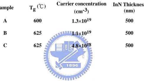
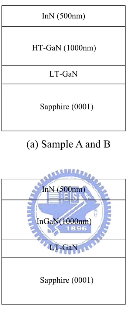
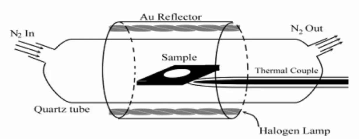
these InN epilayers shows an unintentional doping. The InN epilayer was grown on InGaN/sapphire (0001) with same layer thickness of 500 nm in order to decrease the carrier concentration and improve quality. The data are list in Table I sample parameters. A schematic diagram of the sample structure was shown in Fig. 3-1. The as-grown InN wafer samples was divided into eleven samples with the same area. They were annealed at different temperature from 450℃~ 750℃ with the anneal time of 30s. The rapid thermal annealing system was shown in Fig.3-2.
Table I Sample parameters
Sample Tg (℃) Carrier concentration
(cm-3) InN Thickness (nm) A 600 1.3×10¹⁹ 500 B 625 1.1×10¹⁹ 500 C 625 4.8×10¹⁸ 500
HT-GaN (1000nm) LT-GaN
Sapphire (0001) InN (500nm)
(a) Sample A and B
InGaN(1000nm) LT-GaN
Sapphire (0001) InN (500nm)
(b) Sample C
Fig. 3-1 Schematic diagram of sample structures: (a) sample A and B (b) sample C.
3.2
Measurement techniques
(a) Micro-photoluminescence (μ-PL) system
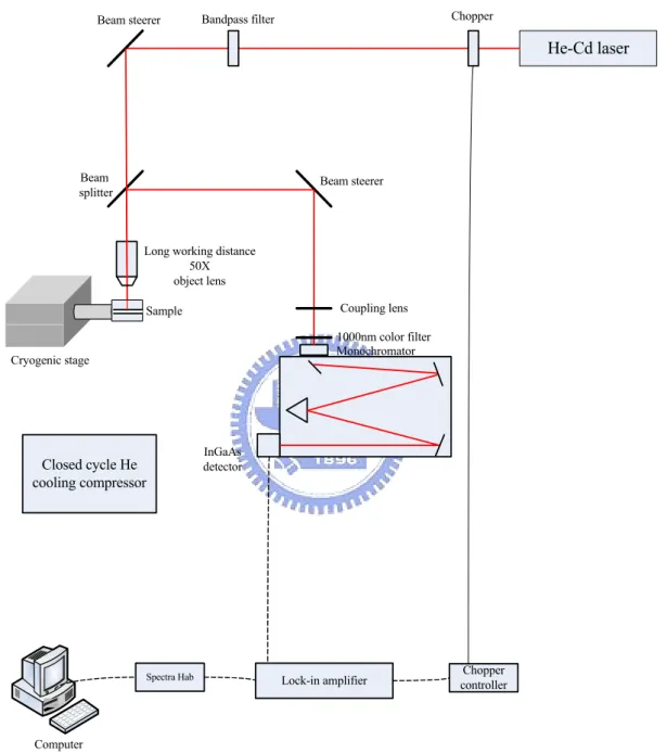
The micro-PL system incorporated an Olympus optical microscope. A schematic of set-up is shown in Fig. 3-3. The He-Cd laser opterating at 442-nm lines was used as the excitation light source with the output power about 95 mW. The beam was reflected by two mirror and then incident into the microscope, passing through a beam splitter and focused by the long working distance near-IR 50X objective lens (Mitutoyo NIR 50X, N.A. = 0.42). The luminescence signals were collected by the objective lens and reflected by the beam splitter. The signals were focused by the lens, with a spot size ≦ 5μm and reflected by two UV-enhance mirrors again. Finally, the PL signals were sent into the monochrometer (ARC Pro 500) and InGaAs photodetector. The signals were amplified by the standard lock-in amplifier (Stanford SR530) and Acton Spectra Hub.
Low-temperature micro-PL measurement was carried out using a closed cycle cryogenic system (APD HC-2D). In this thesis, we will investigate the rapid thermal annealing effect.
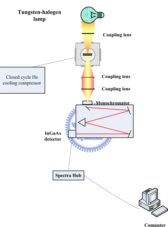
(b) The transmission system.
For the transmission measurements, the sample was mounted on the sample holder of a closed-cycle cryostat. A broad band tungsten-halogen lamp was used as a light source. The incident beam was
focused on the sample by the coupling lens. Optical signals were sent into the monochrometer (ARC Pro 500) and InGaAs photodetector. Experimental setup is shown in Fig. 3-4.
He-Cd laser
Lock-in amplifier controllerChopper
Spectra Hab Chopper Bandpass filter Beam steerer Coupling lens 1000nm color filter Beam steerer InGaAs detector Long working distance
50X object lens Sample Monochromator Beam splitter Computer Cryogenic stage Closed cycle He cooling compressor
Chapter 4 Results and Discussion
In this chapter, we used the photoluminescence (PL) spectra and absorption spectra to study the optical properties of InN epilayers with carrier concentration in the range from 4.8×1018cm-3 to 1.3×1019cm-3 and the effects of rapid thermal annealing.
4.1 Emission and absorption properties of InN epilayers
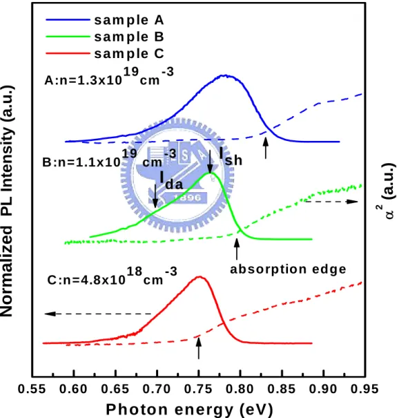
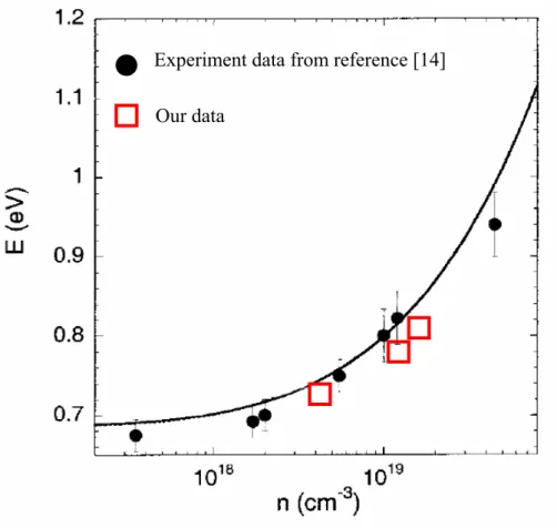
Fig. 4-1 shows the photoluminescence and absorption spectra of n-InN samples with carrier concentration from 1.3×10¹⁹ to 4.8×1018cm-3. As the carrier concentration increases, the PL peak energy (0.741~0.798 eV) and optical absorption edge (0.751~0.824 eV) shifts toward higher energy, at the same time the full width at half maximum (FWHM) (67~89 meV) increases. These phenomena wereattributed to the strong Burstein-Moss effect. In addition, the PL line shape is highly asymmetric, and it can be explained by the existence of the deep acceptors and shallow acceptors [13]. Furthermore, in degenerate semiconductor, the absorption process is attributed to the transition from the valence band states to the Fermi surface of conduction band. Consequently, the absorption edges are larger than the PL peak energies as shown in Fig. 4-1. In order to understand the relationship between the absorption edge and the carrier concentration, our experimental values were compared with the theoretical calculation in Fig. 4-2. The solid line is the calculated band gap assuming a non-parabolic dispersion for the conduction band and including the band-renormalization effects [14]. The solid circles in Fig. 4-2 are
experimental data observed by J. Wu et al [14] and the open squares are absorption edges of our samples at room temperature. Our experimental data are consistent with the theoretical ones.
C :n =4.8x1018cm-3 B :n =1.1x1019 cm-3
I
d a ab so rp tio n ed g e 0.55 0.60 0.65 0.70 0.75 0.80 0.85 0.90 0.95 α 2(a
.u.)
N
o
rm
a
liz
e
d PL Inte
ns
ity
(a
.u.)
P h o to n en erg y (eV )
s a m p le A s a m p le B s a m p le C A:n = 1.3x1019cm-3I
shFig. 4-1 PL (solid lines) and absorption (dashed lines) spectra of InN epilayers measured at low temperature.
Experiment data from reference [14]
Our data
Fig. 4-2 The relationship between absorption edge and the carrier concentration compared with the theoretical calculation given in reference. Open squares are our data.
4.2 Rapid thermal annealing on InN epilayers
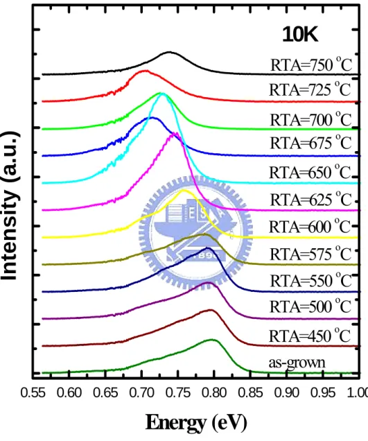
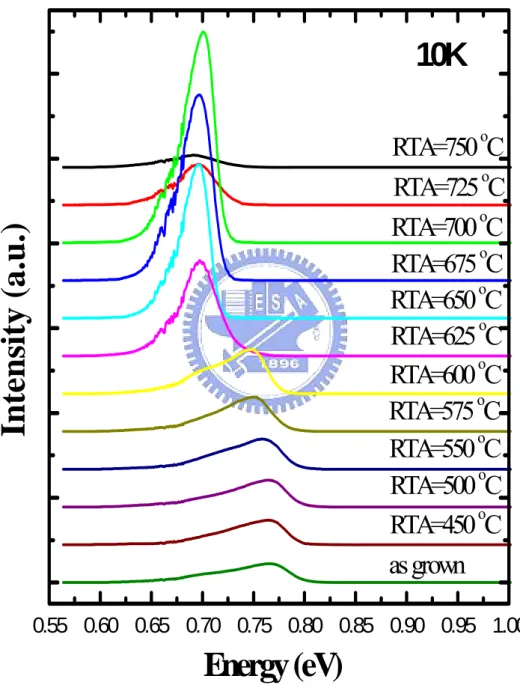
In this section, we study the effects of rapid thermal annealing (RTA) on the optical properties of InN epilayers. In order to understand the RTA effects, we used the PL spectroscopy to study the optical properties of InN before and after annealing. Fig 4-3(a) to (c) show the PL spectra of the InN epilayer after annealing compared with that of as-grown samples. We observed a PL peak energy red-shift, a decrease in FWHM and an increasing integrated PL density as the RTA temperature was increased. The peak energy red-shifts from 0.798 to 0.710, 0.763 to 0.696, and 0.741 to 0.664 eV for sample A, B and C, respectively. The FWHM decreased from 106 to 60 meV, 70 to 30 meV and 67 to 44 meV for sample A, B and C, respectively. We further use two Gaussian functions to fit the PL line shape and the energy difference between these two fitting peaks coincides with the energy difference between the deep acceptor and shallow acceptor. Consequently, the decreasing of FWHM could be attributed to the suppression of deep acceptor as shown in Fig. 4-4. The decreasing of FWHM and the increasing of PL integrated intensity indicated that the improvement of the optical quality due to suppressed the deep acceptor transition and reducing the non-radiative center and the rearrangement mechanism of crystallites in the InN epilayer [10, 12]. In order to further study the mechanism of PL spectra and carrier quenching, we compare the temperature dependence of integrated PL intensity of the as-grown and the rapid thermal annealing at 650℃ of sample B as shown in Fig. 4-5. These data can be theoretically fitted by the Arrhenius equation. The solid line is the fitting of Arrhenius equation [15], involving two
activation mechanisms as follows: T k E T k Ea B
C
e
a Be
C
I
T
I
/ 2 / 1 0 2 11
)
(
− −+
+
=
,where, I(T) and I0 are the respective integrated PL intensities at
temperature T and 10 K, C1 and C2 are fitting constant, and Ea1 and Ea2
are the thermal activation energies which domain at the low and high temperature region respectively. From the fitting results , we obtained that the activation energy at the low temperature range (Ea1) is around 7~8
meV for the as-grown and annealing sample at 650℃ respectively. The result is consistent with the reported shallow acceptor binding energy (Esh)
of about 5~10 meV. Ea2 is 61 mev for the as-grown sample and 57 meV
for the RTA sample at 650℃ at high temperature range. The result was also close to Eda of about 50 - 55 meV which was identified as the
transition from the degenerate electrons to the deep acceptors. The activation energy may be attributed to holes thermally de-trapped from the shallow or deep acceptor states into valance band [13].
In order to futher identify the mechanism of spectra variation, Hall measurement was carried out for sample B as shown in Fig. 4-6(a). It clearly reveals that the annealing treatment partly improves the electrical properties, especially for carrier concentration. The carrier cocentration decreases from 1.1×1019 cm-3 to 2.8×1018 cm-3 for the as grown and the RTA sample at 650℃ respectively. The result is consistent with the absorption edge measurement for different RTA temperature as shown Fig. 4-6(b). Typical absorption curves (square of absorption coefficient versus photon energy) are shown in the insert of Fig. 4-6(b). To explore
the effect of carrier concentration on the absorption edge, the absorption edge was plotted as a function of carrier concentration with a theoretical calculation represented by a solid curve in Fig. 4-7. Our experiment data are consistent with the theoretical prediction.
The dependence of Fermi surface in the conduction band on the carrier concentration was also studied. The Fermi energy of the parabolic electron band [16, 17] can be described as follows:
3 2 18) 10 )( ( 58 . 3 n m m E e o F =
where me is the effective mass of an electron, mo is the free-electron mass
and EF is Fermi energy. Assuming the effective mass linearly increases as
[18], ) / ) ( 1 ( E E E0 m me = Γ + − g
where mΓ is the electron effective mass at the Γ point, and E0 is the
kinetic energy at which the effective mass doubles. The dependence Fermi energy on carrier concentration can be then expressed as
(
3.58/)(
/)
(
/10)
1/4] 1/2} {[ 18 2/3 1/2 0 0 + − =E E m mΓ n EF oThis equation considers the non-parabolic band through the use of the liner dependence of effective mass.
For sample B, the carrier concentrations are n = 1.1×1019 cm-3 and n = 2.8×1018 cm-3 for the samples of as grown and RTA at 650℃, respectively. Their respectively calculated Fermi energies (EF) are 185 meV and 99
to the difference of optical absorption edge, 81meV, between as grown and RTA at 650℃ of sample B. This result further corroborates the fact that the energy difference in absorption edge is due to the Burstein-Moss shift.
0.55 0.60 0.65 0.70 0.75 0.80 0.85 0.90 0.95 1.00
Inte
ns
ity
(a
.u.)
Energy (eV)
as-grown
RTA=450
oC
RTA=500
oC
RTA=550
oC
RTA=575
oC
RTA=600
oC
RTA=625
oC
RTA=650
oC
RTA=675
oC
RTA=700
oC
RTA=725
oC
RTA=750
oC
10K
Fig. 4-3(a): PL spectra of the InN epilayer for sample A at different RTA temperatures.
0.55 0.60 0.65 0.70 0.75 0.80 0.85 0.90 0.95 1.00
Intensity (a.u.)
Energy (eV)
as grown
RTA=450
oC
RTA=500
oC
RTA=550
oC
RTA=575
oC
RTA=600
oC
RTA=625
oC
RTA=650
oC
RTA=675
oC
RTA=700
oC
RTA=725
oC
RTA=750
oC
10K
Fig. 4-3(b): PL spectra of the InN epilayer for sample B at different RTA temperatures.
0.55
0.60
0.65
0.70
0.75
0.80
0.85
0.90
Intensity (a.u.)
Energy (eV)
10K
as grown
RTA=450
oC
RTA=500
oC
RTA=550
oC
RTA=575
oC
RTA=600
oC
RTA=625
oC
RTA=650
oC
RTA=675
oC
RTA=700
oC
RTA=725
oC
RTA=750
oC
Fig. 4-3(c): PL spectra of the InN epilayer for sample C at different RTA temperatures.
0.6 0.7 0.8 0.9 1.0 Intensity (a.u.) E nergy (eV ) as-grow n (a) 0.6 0.7 0.8 0.9 1.0 Intensity (a.u.) Energy (eV) RTA-650oC (b)
Fig. 4-4: PL spectra for sample B at 10K, (a) as-grown (b) RTA-650℃. The solid lines are the Gaussian fitting curves, and the circles are the PL data
0 10 20 30 40 50 60 70 In te grated PL Int e n sit y ( a.u.) 1000/T(1/K) As-grown (a) Ea2=61±13meV Ea1=8±1meV 0 2 0 4 0 6 0 8 0 1 0 0 Int e g r a ted P L In te nsi ty (a .u. ) 1 0 0 0 /T (1 /K ) R T A -6 5 0 o C (b ) Ea1=7±1meV Ea2=57±10meV
Fig. 4-5: Temperature dependence of the integrated PL intensity of sample B for (a) as-grown and (b) RTA-650℃.
450 500 550 600 650 2 4 6 8 10 12 14 Carrierc o n ce n teatio n
(
10 18 cm -3)
RTA Temperature(
oC)
as-grown(a)
450 500 550 600 650 0.64 0.66 0.68 0.70 0.72 0.74 0.76 0.78 as-grownAbsorption Edge (eV)
RTA Temperature
(
oC)
(b) 0.6 0.7 0.8 0.9 0.0 5.0x10⁸ 1.0x10⁹ 1.5x10⁹ α 2 ( cm -2 ) Energy (eV) as-grown RTA-650oCFig. 4-6 (a) Carrier concentration versus RTA temperature, (b) absorption edge as a function of RTA temperature for sample B. The typical absorption curves (square of absorption coefficient) are shown in the inset of (b).
Our data
Experiment data from reference [14]
Fig. 4-7: Absorption edge as a function of carrier concentration. The solid curve is a theoretical calculation from reference 14. Open squares are our data points for different annealing temperatures from 450℃ to 650℃.
Chapter 5 Conclusions
In this thesis, we investigated the optical properties of InN epilayers with carrier concentration from 1.3×10¹⁹ to 4.8×1018cm-3. The PL and absorption edge of the InN epilayers show blue-shift in energy due to the Burstein-Moss effect. Our experiment data are consistent with the theoretical calculation of band gap which assumes a non-parabolic dispersion for the conduction band and including the band gap-renormalization effects. Furthermore, we studied the effect of RTA on the physical properties of InN epilayers. RTA results in a significant decrease in carrier concentration and full width at half maximum of PL spectra. Besides, the integrated PL intensity also increases after the RTA process. The temperature dependence of the integrated PL intensity of the InN epilayers is shown by the Arrhenius plot. Two activation energies were obtained. We ascribe them to the deep acceptor and shallow acceptor-related transitions. The former is related to the hole binding energy of 50 ~ 55 meV form the deep acceptors level to valence band top. The latter is attributed to the hole binding energy of 5 ~ 10 meV from the shallow acceptors to the valence band top. The asymmetric PL line shape became more symmetric after RTA process, it is attributed to the suppression of deep acceptor level.
References
[1] T. L. Tansley and C. P. Foley, J. Appl. Phys. 59, 3241 (1986).
[2] T. Matsuoka, H. Okamoto, M. Nakao, H. Harima, and E. Kurimoto, Appl. Phys. Lett. 81, 1246 (2002).
[3] J. Wu, W. Walukiewicz, W. Shan, K. M. Yu, J. W. Ager III, S. X. Li, E. E. Haller, H. Lu, and W. J. Schaff. J.Appl Phys. 94, 4457 (2004). [4] J. Wu, W. Walukiewicz, K. M. Yu, J. W. Ager III, E. E. Haller, H.
Lu, W. J. Schaff, Y. Saito, and Y. Nanishi, Appl. Phys. Lett. 80, 3967 (2002)
[5] S. P. Fu and Y. F. Chen, Appl. Phys. Lett. 85, 1253 (2002)
[6]C. Stampfl, C. G. Van de Walle, D. Vogel, P. Kruger, and J. Pollmann, Phys. Rev. B 61, R7846 (2000).
[7]S. Limpijumnong and C. G. Van de Walle, Phys. Status Solidi B 228, 303(2001).
[8]T. L. Tansley and R. J. Egan, Phys. Rev. B 45, 10942 (1992).
[9]K. S. A. Butcher, M. Wintrebert-Fouquet, P. P.-T. Chen, T. L. Tansley, and H. Dou, S. K. Shrestha and H. Timmers, M. Kuball, K. E. Prince, J. E. Bradby, J. Appl. Phys. 95, 6124 (2005).
[10] H. Lu, W. J. Schaff, J. Hwang, H. Wu, W. Yeo, A. Pharkya, and L. F. Eastman, Appl. Phys. Lett. 77, 2548 (2000).
[11] H. Lu, W. J. Schaff, L. F. Eastman and C. E. Stutz, Appl. Phys. Lett. 82, 1736(2003).
[12] Q. X. Guo ,T. Yamamura, A. Yoshida and N. ltoh, J. Appl. Phys.
[13] A. A. Klochikhin, V. Yu. Davydov, V. V. Emtsev, A. V. Sakharov, V. A. Kapitonov, B. A. Andreev, H. Lu and William J. Schaff. Phys. Rev. B 71, 195207 (2005).
[14] J. Wu, W. Walukiewicz, W. Shan, K. M. Yu, J. W. Ager III, E. E. Haller, H. Lu, and W. J. Schaff. Phys. Rev. B 66, 201403 (2002). [15] Y. H. Wu, K. Arai, and T. Yao, Phys. Rev. B 53, 10485 (1996).
[16]V. Yu. Davydov, A. A. Klochikhin, V. V. Emtsev, D. A. Kurdyukov, S. V. Ivanov, V. A. Vekshin, F. Bechstedt, J. Furthmuller, J. Aderhold, J. Graul, A. V. Mudryi, H. Harima, A. Hashimoto, A. Yamamoto, and E. E. Haller, Phys. Status Solidi B 234,787 (2002) [17] D. Olego and M. Cardons, Phys. Rev. B 22, 15 (1979).