由哺乳類動物視網膜生物模型所設計之金氧半仿視網膜晶片
68
0
0
全文
(2) 由哺乳類動物視網膜生物模型所設計之 金氧半仿視網膜晶片. A CMOS RETINAL CHIP BASED ON THE BIOLOGICAL MODEL DERIVED FROM THE MAMMALIAN RETINA. 研 究 生:楊文嘉. Student:Wen-Chia Yang. 指導教授:吳重雨. Advisor:Chung-Yu Wu. 國 立 交 通 大 學 電子工程系電子研究所 碩 士 論 文 A Thesis Submitted to Institute of Electronics College of Electrical Engineering and Computer Science National Chiao Tung University in Partial Fulfillment of the Requirements for the Degree of Master in Electronic Engineering July 2004 Hsinchu, Taiwan, Republic of China. 中華民國九十三年七月.
(3) 由哺乳類動物視網膜生物模型所設計之 金氧半仿視網膜晶片 研究生:楊文嘉. 指導教授:吳重雨. 國立交通大學. 電子工程學系電子研究所碩士班. 摘要 ABSTRACT (CHINESE) 於本論文中,我們提出一個依據由哺乳類動物視網膜建立之生物模型所設計的 仿視網膜矽晶片;文中亦詳論其特性與工作原理。一原本應用於細胞非線性網路機 器(CNN-UM)的生物模型為此仿視網膜晶片的基礎架構;晶片之功能為模仿哺乳類動 物視網膜內的光受器(photoreceptor)及水平細胞(horizontal cell)。 此晶片包含一個大小為32x32,可實現光受器及水平細胞功能的影像感測陣 列;陣列中包含了許多完全相同的基本單元。每個基本單元中又包含四個主要部份: 光輸入元件、光受器一、光受器二與水平細胞元件。晶片中還包括了輸出、輸入接 墊(I/O pads)的靜電防護與位址解碼(Address decoder)及訊號讀出等電路。 藉由一維陣列的電路模擬(HSPICE)結果,我們驗證此晶片在空間域及時域的特 性;而實際的二維感測陣列則利用0.35微米金氧半矽製程製造,用來測試實際的晶 片反應。最後,我們比較原本生物模型的結果與電路模擬及實際電路量測的結果之 異同以檢驗此晶片的正確性與待改進之處。. i.
(4) A CMOS RETINAL CHIP BASED ON THE BIOLOGICAL MODEL DERIVED FROM THE MAMMALIAN RETINA Student: Wen-Chia Yang. Advisor: Chung-Yu Wu. Department of Electronics Engineering & Institute of Electronics National Chiao Tung University. Abstract ABSTRACT (ENGLISH) In this thesis, a retinal chip based on the biological model derived from the mammalian retina is proposed. The CMOS compatible retinal chip is designed based on the biological retinal model originally established for the implementation on CNN Universal Machine (CNN-UM) to mimic the functions of the photoreceptors and the horizontal cell and other cells in mammalian retina. The retinal chip contains a focal plane sensory array of 32x32 similar basic cells that perform the functions of photoreceptor and the horizontal cell. Each basic cell contains four main parts: photo-input, PH1, PH2, and the horizontal. ESD protection circuit for I/O pads, address decoder and other readout circuits are also included in this chip. Spatial and temporal characteristics of a one-dimensional array are verified via HSPICE simulations, while a two-dimensional array of 32x32 cells is fabricated to investigate the space-time pattern that this chip appears with subjected to a certain stimulus. The retinal chip is fabricated in 0.35µm double-poly triple-metal CMOS process. The results of HSPICE simulation and chip measurement are compared with that of the original biological model to examine the consistency and the difference for further improvements.. ii.
(5) ACKNOWLEDGEMENT 本篇論文的完成,要歸功於許多人的協助與支持。首先要感謝不吝 教導我的指導老師吳重雨教授,感謝他細心的指導,若無老師耐心的指 正與鼓勵,這篇論文不可能呈現給諸位。另外我要特別感謝經常給予我 協助與指導的林俐如學姊及黃冠勳學長,除了提供論文相關的資料與建 議外,對於我的研究方向與未來規劃,學長姐也熱心地提供了建議與分 析。 再來要感謝我的家人;父親楊長琴先生、母親何詠媛女士以及弟弟 楊文棟先生。感謝他們無怨無悔的照顧、支持與鼓勵,使我能順利完成 學業與此論文。 最後感謝提供晶片製造環境的工研院電子所,他們的協助使本論文 得以順利產生。對於其他在我身邊曾經幫助過或鼓勵過我的朋友們,一 樣地致上深深的感謝之意。 謹以此論文獻給所有關心我的長輩、家人、同學及朋友。. 楊文嘉 國立交通大學 新竹台灣 2004 年 7 月. iii.
(6) CONTENTS ABSTRACT (CHINESE) .................................................................................................. i ABSTRACT (ENGLISH)................................................................................................. ii ACKNOWLEDGEMENT............................................................................................... iii CONTENTS...................................................................................................................... iv TABLE CAPTIONS.......................................................................................................... v FIGURE CAPTIONS ...................................................................................................... vi CHAPTER 1 INTRODUCTION .................................................................................. 1 1.1 BACKGROUND .............................................................................................. 1 1.1.1 MORPHOLOGY AND PHYSIOLOGY OF RETINA........................... 1 1.1.2 THE CNN MODEL ................................................................................ 3 1.2 RESEARCH MOTIVATION AND ORGANIZATION OF THIS THESIS 4 1.2.1 RESEARCH MOTIVATION .................................................................. 4 1.2.2 THESIS ORGANIZATION .................................................................... 4 CHAPTER 2 CIRCUIT DESIGN OF THE RETINAL CHIP................................... 8 2.1 ARCHITECTURE OF A BASIC CELL OF THE RETINAL CHIP .......... 8 2.2 CIRCUIT DESIGN OF THE BASIC CELL ............................................... 10 2.2.1 THE PHOTO-INPUT ........................................................................... 10 2.2.2 THE PHOTORECEPTOR-1................................................................. 12 2.2.3 THE PHOTORECEPTOR-2................................................................. 12 2.2.4 THE HORIZONTAL ............................................................................ 15 2.2.5 IMPACTS OF DEVICE LEAKAGE AND MISMATCH ................... 15 2.3 ARCHITECTURE OF 2-D RETINAL ARRAY ......................................... 16 2.4 SIMULATION RESULTS............................................................................. 17 CHAPTER 3 LAYOUT DESCRIPTIONS AND EXPERIMENTAL RESULTS... 38 3.1 LAYOUT DESCRIPTIONS.......................................................................... 38 3.2 EXPERIMENTAL ENVIRONMENT ......................................................... 39 3.3 EXPERIMENTAL RESULTS ...................................................................... 40 CHAPTER 4 CONCLUSIONS AND FUTURE WORKS ....................................... 54 4.1 CONCLUSIONS ............................................................................................ 54 4.2 FUTURE WORKS......................................................................................... 54 REFERENCES................................................................................................................ 56 VITA................................................................................................................................. 58. iv.
(7) TABLE CAPTIONS Table I Table II. The designed device dimensions in the retinal basic cell. Summary of characteristics of the proposed 32x32 retinal chip.. v.
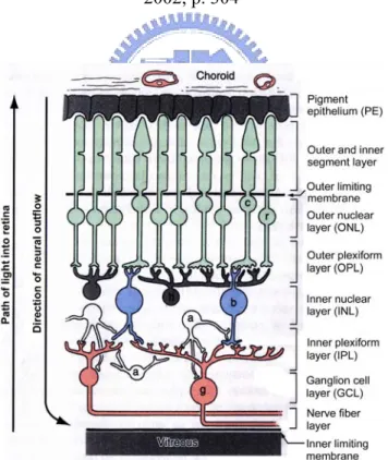
(8) FIGURE CAPTIONS Fig. 1. Cross section of the human eye. The gray arrow shows the path of light through the optical apparatus. Reprinted from “Fundamental Neuroscience,” by D. E. Haines, Fig. 2. The cross section of the human retina. The labels c, r, h, b, a, and g indicate cones, rods, horizontal cells, bipolar cells, amacrine cells, and ganglion cells respectively. Reprinted from “Fundamental Neuroscience,” by D. E. Haines, 2002, p. 306. Fig. 3. Interactions in the outer plexiform layer of the retina. Label C, H, and B indicate cone, horizontal cells and bipolar cell respectively. Reprinted from [6]. Fig. 4. The CNN model of outer and inner plexiform layer including cone cells, horizontal cells, bipolar cells, amacrine cells, and ganglion cells. The horizontal line represents a kind of neuron type. Vertical line indicates an interaction between layers. Reprinted from [7]. Fig.5. Equivalent block diagram of the outer retina in the CNN model. D and τ represent space and time constant respectively. The units for D and τ are µm and ms respectively. Fig. 6. The actual architecture of our basic cell. τ is the time constant and D is the diffusion constant. Fig. 7. The transient simulated result of the CNN model. (a) The input signal, (b) the output of PH1, (c) the output of PH2. Fig. 8. The simulated space-domain response of the CNN model. (a) The input signal, (b) output of the horizontal, (c) the output of PH1. Fig. 9. Simulated transient responses of the model with different diffusibility of the horizontal applied. The time constant of PH2 is kept to be 0.25ms in the simulation. Fig. 10. Simulated transient responses of the model with different time constant of PH2 applied. The space constant of the horizontal σ is kept to be 50 in the simulation. Fig. 11. Simulated space-domain response of the model with different diffusibility of the horizontal applied.(a)Output of the horizontal, (b) output of PH1. Fig. 12. The circuit of a basic cell constructed from the architecture in Fig. 6.The arrows represent the four current outputs. IIn, IPH1, IH, and IPH2 are for the output of photo-input, PH1, horizontal, PH2 respectively.. vi.
(9) Fig. 13. The current conveyor. (a) The block diagram of a current conveyor, (b) the schematic of an example of current conveyor. Fig. 14. Current delay element. (a) The circuit of a current delay element, (b) the small signal equivalent circuit of the current delay element. Fig. 15. The architecture of the 2-D retinal array and other peripheral circuits. Fig. 16. The schematic of the address decoder used in the chip. Fig. 17. The output buffers of the chip. (a) Output buffer for PH1, PH2, and the horizontal, (b) output buffer for the photo-input. Fig. 18. HSPICE simulated transient response in the condition that Vbias1=1.5V, Vbias2=0.6V, Vbias3=1.1V, Vbias4=430mV, Vsm=1.1V. The stimuli is a pulse with 100pA transient current added to an 100pA background induced DC current. A virtual background current of 1.2nA is supplied. The simulated results of (a) photo-input, (b) PH1, (c) PH2, (d) the horizontal. Fig. 19. HSPICE simulated transient response in the condition that Vbias1=1.5V, Vbias2=0.6V, Vbias3=1.1V, Vbias4=0, Vsm=1.1V. The stimuli is a pulse with 100pA transient current added to an 100pA background induced DC current. No virtual background current is supplied. The simulated results of (a) photo-input, (b) PH1, (c) PH2, (d) the horizontal. Fig.20. HSPICE simulated transient response in the condition that Vbias1=1.5V, Vbias2=0.6V, Vbias3=1.1V, Vbias4=530mV, Vsm=1.1V. The stimuli is a pulse with 100pA transient current added to an 100pA background induced DC current. A virtual background current of 11.6nA is supplied. The simulated results of (a) photo-input, (b) PH1, (c) PH2, (d) the horizontal. Fig. 21. Simulated time constant with different I D ,MP 7 supplied. Fig. 22. The steady-state space response when the middle six cells are turned on. (a) Photo-input, (b) output of the horizontal, (b) output of PH1. The simulation is performed under the condition that Vbias1=1.5V, Vbias2=0.6V, Vbias3=1.1V, Vbias4=430mV. A virtual background current of 1.2nA is supplied. Fig. 23. HSPICE-simulated spatiotemporal patterns of the circuit. The time axis is located on the bottom and the space axis is on the left. The right most color bar in (c) shows the mapping from normalized to assigned color. Space-time pattern of (a)PH1, (b) the horizontal, (c) PH2.. vii.
(10) Fig. 24. Layout of the whole retinal chip. Main parts of the chip are labeled. Sensory array is in the center, the row and column address decoders are in the upper and left of the array respectively. Output buffer and address buffer are also labeled. Fig. 25. Layout and floorplan of a basic cell of the sensory array. The four regions of main parts of the basic cell are surrounded by solid lines. The lower two sub region surrounded by dashed lines are phototransistor and PMOS capacitor MP10. Fig. 26. Photograph of the whole retinal chip. Main parts of the chip are labeled. Sensory array is in the center, the row and column address decoder are in the upper and left of the array respectively. Output buffer and address buffer are also labeled. Fig. 27. Photograph of a basic cell. Only the photo-BJT region is not covered by metal. Fig. 28. The measurement setup diagram. Fig. 29. Measured transient response. Curve (a) the output of photo-input (b) PH2 (c) PH1 (d) horizontal. Under bias condition: Vbias1=1.52V, Vbias2=0.62V, Vbias3=1.11V, Vbias4=25mV, Vsm=1.26V. Fig. 30. Comparison of the chip measured transient response to the model simulation results and HSPICE simulation results. (a) PH1, (b) PH2, (c) horizontal. The time units for model simulation and SPICE simulation are the same, 10µs/frame; time unit for chip measurement is 20µs/frame. Fig. 31. Measured transient response with different Vbias3.. Under bias: Vbias1=1.5V, Vbias2=0.65V, Vbias4=20mV, Vsm=1.3V. Fig. 32. Measured time constant calculated from rise and fall time of PH2. IPH2 represents the DC level of output of PH2. Fig. 33. Measured spatial response. (a) Photo-input, (b) the output of horizontal, (c) PH1. Under bias condition: Vbias1=1.5V, Vbias2=0.65V, Vbias3=1.2V, Vbias4=312mV Fig. 34. Comparison of the chip measured spatial response to the model simulation results and HSPICE simulation results. (a) Photo-input, (b) horizontal, (b) PH1. Fig. 35. The measured spatiotemporal pattern of the chip. (a) PH1, (b) Horizontal. The output current is normalized and then color-coded according to the bottom-right colorbar. Fig. 36. The space-time pattern of (a) OFF bipolar cell, (b) horizontal cell layer measured from real retinas. Reprinted from [5]. viii.
(11) CHAPTER 1. INTRODUCTION. 1.1. BACKGROUND. 1.1.1 MORPHOLOGY AND PHYSIOLOGY OF RETINA The Retina is the early processing unit in the visual nervous system of the vertebrate [1]. It analyzes and interprets the visual world by sending the brain dozens of different space-time representations containing all the information we need to comprehend the visual world. These representations constitute a fundamental visual language that is elaborate on at the higher centers in the brain [2]. The retina is a tiny tissue lying on the bottom of eye chamber as shown in Fig. 1. Incoming light is first focused on the retina by the lens, and the retina takes over the reception and initial processing of the visual signal [3]. The retina is composed of the neural retina and the retinal pigment epithelium, as shown in Fig. 2. The commonly used term, inner retina, refers to structure located toward the vitreous, and the other one, outer retina, is used in reference to structure s located toward the pigment epithelium. Incoming light is incident from the bottom of vitreous and can passes through the cells above because they are transparent. The neural retina contains the photoreceptors and other types of neuron for light sensation and processing. There are two types of photoreceptors in retina, the cones and the rods. The human retina contains approximately 120 million rod cells and 6 million cone cells. Cones almost completely occupied the central part of the retina, named fovea, and the rods dominate the peripheral region. The rod cells named for the shape of their. 1.
(12) outer segment are responsible primarily for achromatic and night vision while the cone cells are good at color and bright vision [3]. The photoreceptors absorb photons and convert them to an electrical signal. The signals from the photoreceptors are received by two types of the inter-neurons in the retina, that is, the bipolar cells and the horizontal cells. The cone changes its state and output by chemical mechanisms [1]. In the dark, the cone is at the resting state. At this state, the sodium channels on the membrane of the cone are open and the cone’s membrane potential keeps a high resting level of about -40mV. The cone is called to be depolarized in this situation. When the cone is illuminated the opsin in the cone absorbs photons and undergoes a conformational change which results in the closure of the sodium channels and causes the membrane potential of the cone to fall toward more negative value. In the absolute sense the output signal of the cone increases with the increase of the incident light. The cone is said to be hyperpolarized in this condition. The horizontal cells make connections to both photoreceptors and bipolar cells through the triad synapse. Each horizontal cell is also connected to its neighbors by gap junctions through which ions could diffuse [1]. The horizontal cell gets the output of the cone as its input and diffuses it out to the neighboring horizontal cells through gap junctions. The potential of any given horizontal cell is thus determined by the spatially weighted average of its own potential and the potentials of other horizontal cells around it. Nearby cells make the strongest contribution and the further cells contribute less. Therefore the horizontal cells could be regarded as a spatial low-pass or smoothing filer used commonly in digital image processing system. The output of the horizontal cells is thus the smoothing result of that of the cones which corresponds to the original incident image. This spatial average or smoothing signal is send back to the photoreceptor as an inhibitive signal by depolarization mechanism [3]. The processing of smoothing and depolarization allows horizontal cells to sharpen the edge of incoming image and thus enhance the contrast. The sketch of such mechanism is shown in Fig. 3. The signal from photoreceptors and horizontal cells are used to generate graded potential signal by bipolar and amacrine cells [3]. All these signals with visual information are feed to ganglion cells to produce spiking signals that carry useful edge or. 2.
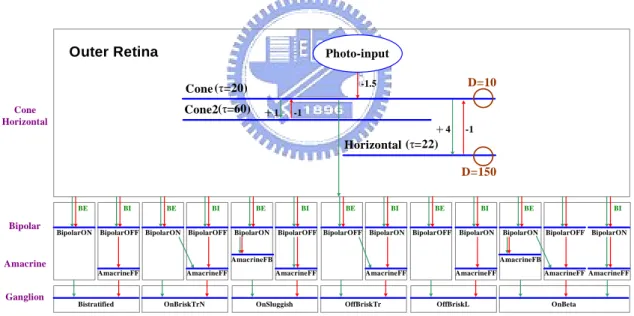
(13) motion information. Ganglion cells are the output of the retina and their axons converge on the optic disc and form the optic nerve that transmits the visual information to the visual cortex of the brain. 1.1.2 THE CNN MODEL With increasing understanding of mammalian retinas, more functions of various kinds of retinal cells have been revealed [4] [5]. A cellular neural/non-linear network (CNN) model for the mammalian retina under light-adapted conditions has been presented [2]. This model is aimed at being capable of implementation on CNN Universal Machine (CNN-UM) chips and is based on anatomical and physiological studies of the rabbit retina [4]. The structure of the model is based on retinal morphology with some structural simplifications that allow low-complexity implementation [6]. The processing structure of the model for CNN is shown in Fig. 4. As mentioned in previous section, the retina contains two major parts, the outer retina and the inner retina. The outer retina is plotted in the upper box of the figure while the inner retina is in the lower. The outer retina is the same for all the different inner retina pathways [7].In the sketch, each horizontal line represents a neuron-type layer. For example, the first two horizontal lines from the top represent the cone and cone2 in retina. Cone2 imitates the self feedback of the cone cell and actually does not exist in the physical retina. The following horizontal line represents the horizontal cell. As for the vertical lines, they represent the interconnections between different neuron-types. For example, cone2 layer acquires its excitatory input from cone layer and sends an inhibitory signal back to the cone layer; the interaction between cone and horizontal is similar. The signed number next to each vertical line represents the gain from one layer to another. Besides, each layer, horizontal line, is associated with a diffusion constant D, also called space constant, and a time constant τ. The space constant represents the intra-layer coupling extent and time constant characterizes the delaying effect. The output of cone layer is fed to On-bipolar and Off-bipolar for further processing. The equivalent block diagram of the outer retina model is shown in Fig.5.. 3.
(14) 1.2. RESEARCH MOTIVATION AND ORGANIZATION OF THIS THESIS. 1.2.1 RESEARCH MOTIVATION The previously described model is proposed for the capability of being implemented on CNN-UM. The CNN-UM is a cellular analog stored-program multidimensional array computer with distributed local analog and logic memory, analoic (analog and logic) computing units, as well as local and global communication and control unit [8]. A complex CNN-UM chip is needed to implement the previous mentioned multilayer model. If a complex multilayer CNN-UM is not available, iterative operations are needed to complete the whole processing of the model, and thus real time processing could not be accomplished. Since the hardware cost of implementation of a complex multilayer CNN-UM is considerably high, we propose a dedicated and less complex chip that realizes part of this model. Since the outer retina is the same for all kind of inner systems, the outer retina must be realized firstly if we want to implement the whole retina structure. In this thesis, a retinal chip that realizes the outer retina of the CNN model is proposed. The model is slightly simplified for chip design. Image sensing devices are also included in our retinal chip so that additional imager like CCD or CMOS imager and the interfaces between CNN-UM and imager are no more needed.. 1.2.2 THESIS ORGANIZATION This thesis is divided into four chapters. The first chapter introduces the background and motivation of this thesis. The architecture and the circuit design of the chip are elaborated in the following chapter. Simulation results of both the biological model and the circuit are also presented in this chapter. Chapter 3 shows the layouts of the chip and the measurement results. In the last chapter, we draw conclusions and bring up the direction of future works.. 4.
(15) Fig. 1. Cross section of the human eye. The gray arrow shows the path of light through the optical apparatus. Reprinted from “Fundamental Neuroscience,” by D. E. Haines, 2002, p. 304. Fig. 2. The cross section of the human retina. The labels c, r, h, b, a, and g indicate cones, rods, horizontal cells, bipolar cells, amacrine cells, and ganglion cells respectively. Reprinted from “Fundamental Neuroscience,” by D. E. Haines, 2002, p. 306.. 5.
(16) Fig. 3. Interactions in the outer plexiform layer of the retina. Label C, H, and B indicate cone, horizontal cells and bipolar cell respectively. Reprinted from [6].. Outer Retina. Photo-input. Cone2(τ=60). Cone Horizontal. D=10. -1.5. Cone (τ=20) +1. -1 +4. -1. Horizontal (τ=22) D=150 BE. Bipolar. BipolarON. BI. BE. BI. BipolarOFF BipolarON. BipolarOFF BipolarON. AmacrineFF. AmacrineFF. BI. BE. BI. BipolarOFF BipolarOFF BipolarON. BE BipolarOFF. BI BipolarON. AmacrineFB. Amacrine. Ganglion. BE. Bistratified. OnBriskTrN. BE BipolarON. BI BipolarOFF BipolarON. AmacrineFB AmacrineFF. OnSluggish. AmacrineFF. OffBriskTr. AmacrineFF. OffBriskL. AmacrineFF AmacrineFF. OnBeta. Fig. 4. The CNN model of outer and inner plexiform layer including cone cells, horizontal cells, bipolar cells, amacrine cells, and ganglion cells. The horizontal line represents a kind of neuron type. Vertical line indicates an interaction between layers. Reprinted from [7].. 6.
(17) PH2 τ=60 Photo-input. τ=20 D=10 PH1. G=-1.5. Output G=4. τ=22 D=150. Horizontal. Fig.5. Equivalent block diagram of the outer retina in the CNN model. D and τ represent space and time constant respectively. The units for D and τ are µm and ms respectively.. 7.
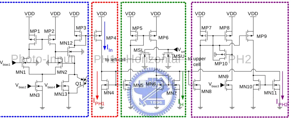
(18) CHAPTER 2. CIRCUIT DESIGN OF THE RETINAL CHIP. 2.1. ARCHITECTURE OF A BASIC CELL OF THE RETINAL CHIP In our design, a number of identical basic cells in an array constitute the retinal chip.. The basic cell is designed following the previously mentioned model derived from biological measurements of the photoreceptor and horizontal cell. The block diagram of the model is shown in Fig.5. In this model, there are two coefficients. τ is the time constant and D is the diffusion constant, also called space constant. τ and D are important parameters of spatio-temporal characteristics of the retina. However each parameter in the model is a relative quantity rather than a fixed one. Actually biological measurement results vary with different test samples. Therefore, our design is focused on realizing comprehensive spatio-temporal characteristics instead of realizing precise coefficients in the model. Thus the actual architecture of the basic cell is slightly modified to the one shown in Fig. 6. The main difference between the actual architecture and the original CNN-model one is that the time constants of PH1 and horizontal are neglected because they are about the same. Besides, the space constant of PH1 is also neglected for its small quantity with respect to that of horizontal. As shown in Fig. 6, there are four major parts in a basic cell, namely, photo-input, photoreceptor-1 (PH1), photoreceptor-2 (PH2), and horizontal (Horizontal). Photo-input, PH1, and PH2 together realize the function of the biological photoreceptor. Photo-input acquires incident signal which is delivered to the other parts of the cell for processing. The PH1 subtracts the output of PH2 and the horizontal from that of the photo-input and makes the result the output of the whole cell. 8.
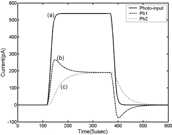
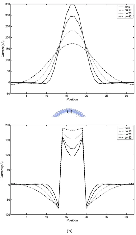
(19) The PH2 acts as a low-pass filter whose input is the output of PH1. PH2 then feeds the low-passed signal back to PH1 for subtraction. If a pulse signal like the one in Fig. 7(a) is applied as the photo-input, the output of PH2 will be like the curve in Fig. 7(c), and then the output of the cell overshoots at the rising edge and undershoots at the falling edge as sketched in Fig. 7(b). This phenomenon obviously arises from the subtraction operation at PH1 and the low-pass operation at PH2. The horizontal mimics the horizontal cell in real retina to perform diffusion of PH1’s signal and feed the diffused signal back to PH1 for subtraction. The horizontal, in fact, realizes the smoothing or blurring function in spatial domain. As illustrated in Fig. 8, (a) is the incident pattern and (b) is the result after the horizontal operation. The six center cells are turned on and the others are turned off. The subtraction at PH1 makes the final output a Mexican-hat-like pattern shown in Fig. 8(c). It could be noticed that the output of PH1 is lowered in the turned-off side and heightened in the turn-on side. Therefore the contrast at the edge is increased with compared to the incident pattern. The processing of horizontal and PH1 enhance the edge of the incident image and make the original image clearer. Fig. 7 and Fig. 8 are the simulated results of the model in Fig. 6. Thirty-two cells constructed according to the model are connected in series to form a 1-D array. The function of PH2 is implemented by a single-pole low-pass filter with the transfer function of. out 1 = in 1 + s • τ 2. (1). The horizontal is achieved by a normalized template that is a discretely sampled Gaussian function in the form ⎛ ( x − µ )2 W ( x, µ , σ ) = exp⎜⎜ − σ2 ⎝. ⎞ ⎟ ⎟ ⎠. (2). The same template is also used in [6] and [7]. In the equation, x is the position of the template, µ the center of the template, and σ is the diffusion constant. The horizontal output of each cell is the weighted average of its input and adjacent cells’ inputs. The weighing is the Gaussian template presented above. This template controls the diffusion extent of the horizontal. σ is the controlling parameter. With a larger σ , the input. 9.
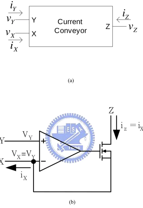
(20) signal could be diffused further. The above and following model simulations are performed using the elements above and the simulation tool is MATLAB Simulink. Fig. 9 shows the influence of varying diffusion constant on the transient response of the model. The middle six cells are turned on for some time and turned off rapidly. The results in Fig. 9 are the outputs from the most center cell. First examine the transient of the horizontal in Fig. 9(c). It could be found that the both of steady-state value and shootings are lower when a larger σ is applied. This is due to the fact that a larger σ makes output of the horizontal the average of a lager area. The signal at one cell could diffuse out further. Therefore the horizontal output of the turned-on cell is averaged to a smaller quantity. Since the output of PH1 plus that of PH2 is the result of subtracting horizontal from photo-input, a smaller horizontal output would make larger PH2 and PH1. As shown in Fig. 9(a), the steady-state value of PH1 increases with the increasing diffusion constant and so does PH2 The simulation result of varying time constant of PH2 is shown in Fig. 10. With a larger time constant, both of PH1 and PH2 need more time to reach their steady state values, but their steady state values are independent of time constant. Fig. 11 shows the simulated spatial response of PH1 and horizontal. It could be found that space constant. σ controls the diffusion range. A larger σ makes a wider diffusion area.. 2.2. CIRCUIT DESIGN OF THE BASIC CELL Fig. 12 shows the circuitry design for the modified architecture mentioned in. previous section. The dimensions of all of the devices in this circuit are listed in Table I. The circuitry is described in detail in the following. 2.2.1 THE PHOTO-INPUT The photo-input is a phototransistor together with a current conveyer used to transduce the incident light into current. The phototransistor is just a parasitic vertical PNP bipolar junction transistor (BJT) in the standard CMOS process with its base floated as represented by Q1. The base region is used to sense the incident light and generate the. 10.
(21) photocurrent. When the light is incident upon the open-base region of the photo-BJT, carriers in this region are generated and photocurrent appears at the emitter. The depletion region of the collector junction has a greater efficiency in generating the carriers for its reverse bias condition when the BJT is in forward active region [9]. Another component in photo-input, current conveyor, is realized by MP1, MP2, MN1, MN2, MN3, and MN12. Current conveyor is a three-port component, as shown in Fig. 13. Fig. 13(a) is the block diagram of a current conveyor. This current conveyor is described by ⎡ iY ⎤ ⎡0 0 0⎤ ⎡vY ⎤ ⎢v ⎥ = ⎢1 0 0⎥ ⎢ i ⎥ ⎢ X⎥ ⎢ ⎥⎢ X ⎥ ⎢⎣ i Z ⎥⎦ ⎢⎣0 ± 1 0⎥⎦ ⎢⎣v Z ⎥⎦. (3). An implementation of current conveyor we use in our design is placing a NMOS transistor in the negative feedback loop of an operational amplifier, as shown in Fig. 13(b). In this configuration, the voltage at X follows that applied to Y, and the current supplied to X is conveyed to the high-impedance output terminal Z.[10] In our circuit, MP1, MP2, MN1, MN2, and MN3 form a differential amplifier used in current conveyor. MN12 is then the NMOS used to convey the current from photo-BJT to the other part of the cell. The current conveyer clamps the emitter of the phototransistor with a voltage close to Vbias1 to prevent the phototransistor from leaving the forward active region. When the light is incident on the base-collector junction of the phototransistor, the photocurrent is generated and amplified by the phototransistor. The induced photocurrent is then mirrored to MP4 through the current mirror formed by MP3 and MP4 from which other elements in the cell could exploit the induced photocurrent for further processing. The transistor MN13 is added in parallel with the phototransistor to provide a constant offset current that is controlled by Vbias4. The photo-input can still work without this offset current. However, during the turn off transient of the incident light the feedback subtractive current from PH2 attempts to force the current of PH1 to be negative as shown in Fig. 7; nevertheless, only when the gate-voltage of MN4, also the drain voltage, be negative could the current of MN4 be negative. Since the source of MN4 is grounded, the lowest allowable voltage of the gate or drain of MN4 is zero. The current is. 11.
(22) impossible to be negative, and the undershooting phenomenon of the cell’s output disappears consequently. Therefore, an additional current source that maintains the operating current in a proper level is necessary to keep proper spatiotemporal characteristics. The offset current added to the input of the cell by MN13 could be viewed as a virtual background illumination since the same offset currents are added to each cell of the chip as a real background lamination affects the chip. Further discussion about MN13 is presented in the following section. 2.2.2 THE PHOTORECEPTOR-1 A couple of current mirrors are used to realize PH1. The photocurrent with offset added is first mirrored from MP3 to MP4, and then flows through transistor MN4 from which the PH2 and the horizontal element could duplicate just the same current via current mirror pairs MN4-MN5 and MN4-MN8. After that, PH2 and the horizontal element are responsible for low-pass and diffusion operations. The output of the horizontal and PH2 are the drain currents of MN6 and MN10 respectively. These two current signals are copied by two current mirror pairs, MN6-MN7 and MN10-MN11. The drains of MN7 and MN11 are connected with that of MN4, and according to Kirchhoff's current law, the sum of output currents of the horizontal and PH1 plus output of PH1 equals to the output current of photo-input, hence the drain current of MN4 equals to photo-input minus the sum of the horizontal and PH2. The result of current subtraction at the drain of MN4 is then the output of a single cell. The foregoing operation accomplishes the self-feedback mechanism of photoreceptors and the feedback mechanism of horizontal cells. In the biological retina, the output of a photoreceptor corresponding to PH1’s output in our design is sent to various kinds of bipolar cells for further processing. 2.2.3 THE PHOTORECEPTOR-2 The function of PH2 is to generate a low-passed signal from PH1’s output with a large time constant coefficient, τ, and then to feed the low-passed signal back to PH1. 12.
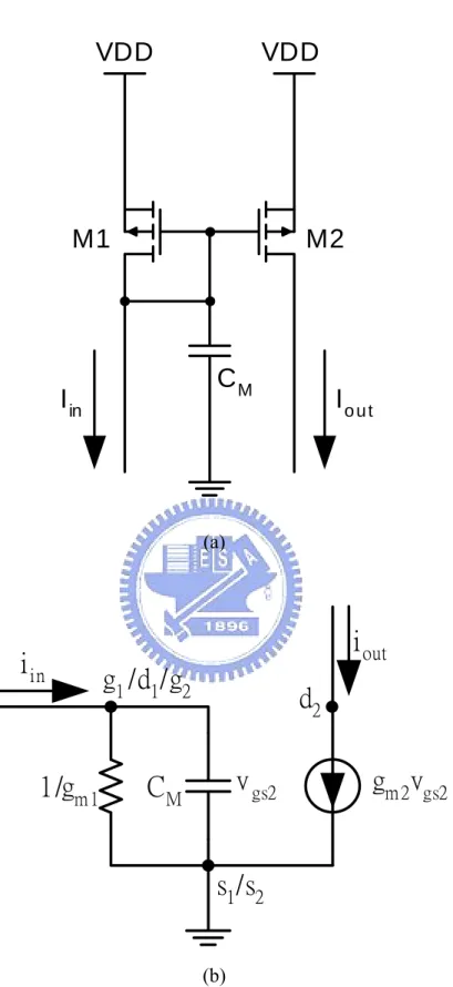
(23) for subtraction. This generates undershoot and overshoot waveforms similar to biological measurements. To realize the architecture, we need a low-pass filter with a large time constant. A circuit named “continuous time current delay element” [11] [12] is used to implement the current-mode low-pass filter. As shown in Fig. 14(a), the current delay element is a current mirror with a capacitor connected between the gates and the sources of the two MOSFET. The small-signal equivalent circuit for this element is sketched in Fig. 14(b). Here we have neglected the output resistance, ro, and all the parasitic capacitances of each MOSFET. From the equivalent circuit, the transfer function of the delay element is described by. iout = iin. g m 2 / g m1 s 1+ g m1 / C M. (4). Here g m1 and g m 2 are the small-signal transconductance of M1 and M2 respectively. The transfer function validates the low-pass characteristic of the delay element. According to the equation, the delay element has a time constant of. τ=. CM g m1. (5). With the constant g m1 , τ is proportional to the capacitance C M . To implement a large time constant needed in the biological model, we need a large capacitor which may occupy quite a large silicon area. A common-source amplifier is exploited to save silicon area and to increase fill factor. The PMOS MP10 with its source and drain tied together is used as a capacitor. To make use of the Miller effect, the capacitor is placed between the input and output of a common-source amplifier constructed by MP8 and MN9 which provides a voltage gain, K. In this way, an enlarged effective capacitance C M ' is obtained. The effective capacitance could be described by C M ' = C MP10 (1 + K ). (6). , where C MP10 is the equivalent capacitance of MP10 and K the voltage gain of the common-source amplifier. If MN9 and MP8 are assumed to be in the subthreshold region,. 13.
(24) the voltage gain K of the common source amplifier could be described by K = g m8, MP8 ro8 // ro 9 =. C OX 1 VT (λ MP8 + λ MN 9 ) C js + C OX. (7). In the above equation, g m ,MP8 represent the small signal transconductance of MN8.. C OX and C js refer to oxide and depletion-region capacitance per unit area respectively. VT is the thermal voltage. λ MP8 and λ MN 9 are the device parameters of MP8 and MN9. Substitute (6) for the C M in (5) yields. τ=. C MP10 (1 + K ) g m , MP 7. (8). g m ,MP 7 represent the small signal transconductance of MN7. About K times silicon area needed to implement the large capacitor without this architecture. However, time constant of this circuit is not absolutely invariable. From equation (8), it could be found that time constant τ is approximately proportional to K and inversely proportional to. g m ,MP 7 with C MP10 being regarded as a constant. Actually g m ,MP 7 are not constant. The small signal transconductance g m ,MP 7 could be describe as. ⎛W ⎞ g m , MP 7 = 2 µ P C OX ⎜ ⎟ I D , MP 7 ⎝ L ⎠ MP 7. (9). when the transistor MP7 is in saturation region, or. g m , MP 7 =. I D ,MP 7 VT. C OX C js + C OX. (10). when MP7 is in weak inversion region [13]. In both (9) and (10), g m ,MP 7 and I D ,MP 7 represent the small signal transconductance and the bias current of MP7 respectively.. C OX and C js refer to oxide and depletion-region capacitance per unit area respectively.. µ P is the mobility of the hole and VT is the thermal voltage. If we assume the transistors in PH2 are all in sub-threshold region and K is far larger than 1, the time constant could be written as. τ=. C MP10 I D , MP 7 (λ MP 8 + λ MN 9 ). 14. (11).
(25) According to (11), the increase of I D ,MP 7 would raise g m ,MP 7 and consequently lower the time constant τ . On the contrary, g m ,MP 7 lowers and τ increases with a smaller bias current I D ,MP 7 . In a word, the constant bias voltage of the circuit could not ensure that the PH2’s time constant keeps constant. With an enlarged equivalent capacitor, MP7 and MP9 form the delay element mentioned above. Finally, another current mirror pair, MN10 and MN11, is in aid of sending back the low-passed signal to PH1. 2.2.4 THE HORIZONTAL The horizontal element imitates an essential part of the biological retina, the horizontal cell, to diffuse out the input signal from PH1 directly from one cell to its adjacent neighbors. Each cell in the proposed 2-D retina structure is connected to their neighboring cells through NMOS transistors, MNR and MNL. All these transistors form the rectangle resistive network. When the current signal acquired from PH1 is delivered to the horizontal element, a four times signal is produced by means of the four times channel width-to-length ratio of the current mirror pair, MP5 and MP6. The amplified current then diffuses through the resistive connection to other cells, and beyond question, the amplified current from vicinal cells could diffuse through the same connection to the very cell simultaneously. The diffusion process is substantially the same as a smoothing function that perform local average of the input signal. The extent of such average is determined by the resistance of the interconnections between cells, which could be controlled by the gate bias, Vsm, of MNR and MNL. The output of the horizontal element, namely the current flowing through transistor MN6, is ultimately mirrored back to the PH1 as well. 2.2.5 IMPACTS OF DEVICE LEAKAGE AND MISMATCH Since we use many current mirrors in our circuit, device mismatches may affect the performance of the chip. However, the goal of our chip is to reproduce response of the real retina qualitatively, and therefore the parameters, time constants and space constant, 15.
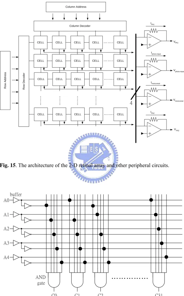
(26) are not necessary to be accurate values. As long as the characteristics of the response of the chip, overshooting and undershooting or smoothing function, are ensured to be correct, device mismatched could be tolerated. Since the photocurrent induced by light is rather small compared to the leakage current of the devices, the input signal must be large enough that the output signal could be observed. If too small input signal is applied, the output current might be affected by leakage currents or noise. The output current might not be observable consequently.. 2.3. ARCHITECTURE OF 2-D RETINAL ARRAY The chip consists of an array of 32x32 pixels, address decoders, and output buffer.. The overall architecture of the chip is shown in Fig. 15. A number of identical basic cells are arranged to form a rectangular array. Two decoders are used to control the output of the cell. The row decoder decodes the m row m. address bits and activates one of 2 row control signals. The column decoder decodes the n. n column address bits and activates one of 2 column control signals. In our design, a 32x32 2-D retina array is designed, and therefore two 5-bit addresses are needed for row and column address to select one cell from all of 32x32 cells. The circuit of the address decoder is shown in Fig. 16. The fundamental block of the address decoder circuit is the five-input and gate. The inputs of each and gate are five non-inverting or inverting address bits, and none of arbitrary two input configurations are the same because an address can only activates one row or one column. The selected address line is set to logic high or the most positive voltage supply of the chip, that is, VDD. Although the final output of the cell is from PH1, each cell in our chip has four output currents, the output of photo-input, PH1, horizontal, and PH2, because these outputs should also be measured to verify the functions of each block. Fig. 17 shows the read out circuit of each basic cell. Each output current of the cell is first reproduced through current mirror with a gain of five. As shown in Fig. 17, M1 could be MP3, MN4, MN6, or MN10 when the output of photo-input, PH1, horizontal, or PH2 is to be read out. The width-length ratio of M2 is five times larger than that of M1, and therefore the actual. 16.
(27) output current is five times of the original one. The amplified current is then fed into two series-connected transistors MSW1 and MSW2 controlled by one of the row signals VR and one of the column signals VC, respectively. Only when both of the VR and VC are set to logic high could the output current be read out. When either of the row or column signal is not activated, one of the switch transistor is turned off and the output current is unable to flow out. Each cell has its own read out circuit, including a current mirror with the gain of five and two NMOS transistors as switches. However, the ends (point B in Fig. 17) of the read out circuit from all of the cells are shorted together to the inverting input of an operational amplifier. Each set of row and column address selects from all of the cells an output current that flows through point B. The current is then converted to voltage signal by another circuit called TIA (Trans-Impedance Amplifier). The TIA contains an operational amplifier and a resistor as shown in the dashed-line region of Fig. 17. A total of four TIAs are needed for the four output currents of each cell. An operational amplifier is connected with an off-chip variable resistor in negative feedback configuration that makes the point B to keep a stable voltage close to Vbias5. The current flowing through the variable resistor is nearly identical to the output current, and the voltage drop across the resistor is proportional to the output current. Accordingly, output from one of the cells could be read out by selecting one row address and one column address and measuring the voltage at the end of the off-chip resistor.. 2.4. SIMULATION RESULTS Thirty-two basic cells describe in the preceding section are connected in series to. form a 1-D array to perform the HSPICE simulation. The following simulation results are all from the simulation using HSPICE model for 0.35µm standard CMOS process. A standard BJT device is used to model the photo-BJT used in real chip. The BJT’s base is each cell’s input to which a base current could be supplied. This base current simulates the photo-stimulus illuminated on the real chip because the base current induces the flow of emitter current proportional to this base current, and furthermore the photo-stimulus similarly induces the emitter current proportional to the intensity of incident light.. 17.
(28) Therefore the input of each cell is a current in the following simulation. First we show the transient response of the circuit when a pulse-stimulus is supplied. Fig. 18 shows the output currents of the center cell of the 1-D array. The simulation is performed under the condition that a pulse signal with a turned-on duration of around 1.2ms is incident on the middle six cells of the array. In the simulation a virtual background illumination current of 1.2nA is added by each cell’s offset transistor MN13. The simulated input to the middle six cells are periodic stimulus with 100pA transient current added to a 100pA background-induced DC current. All other twenty-six cells are supplied with background currents of 100pA. All above-mentioned currents are supplied to the bases of the photo-BJT of all the cells. The output of PH1 in Fig. 18(b) has overshooting and undershooting at the turn-on and turn-off similar to the CNN model simulation results in the previous section. It is also clear in Fig. 18(c) that the output of PH2 appears to be the low-passed output of a pulse signal and the output of the horizontal is analogous to that of the PH1 but has a larger magnitude. Fig. 19 shows transient response of the output currents when the same pulse signal mentioned above is incident on the middle of the array while the transistor MN13 that supplies additional virtual background illumination is turned off. Notice that a background-induced photocurrent of 100pA still exists in this case. Comparing this result with the one in Fig. 18, which is simulated when offset current of 1.2nA is added by MN13; it is clear that the undershooting phenomenon vanished without the aid of MN13 in spite of the background-induced photocurrent exists. In fact, the offset current added mimics the background illumination illuminated on the whole chip. If the intensity of the background illumination is strong enough that the background-induced photocurrent reaches an adequate level to make all the transistors work normally, that is, not being turned off, the offset current provided by MN13 will be no more needed. The additional offset current is only required under weak background illumination. Fig.20 demonstrates the result of simulation under the condition that an overlarge offset current of 11.6nA is supplied. On suchlike condition, the overshooting and undershooting of PH1 no more exist. As discussed in previous section, the time constant of PH2 varies with different bias current of the transistor MP7. The higher level of bias current, I D ,MP 7 , makes lower time constant τ . The disappearance of overshooting and. 18.
(29) undershooting under an overlarge offset current arises from the variation of time constant of PH2. An overlarge virtual background illumination or real ambient illumination results in the increase of the photo-input current which also makes the drain current of MN4 to increase. Therefore, drain current of MN8 which is mirrored from that of MN4 turns out to be larger, and consequently I D ,MP 7 increases and the time constant of PH2 decreases with the larger offset current. As explained in the simulation of the CNN model, the smaller the time constant, the less noticeable the overshooting and undershooting would be. When the time constant is too small that the delayed signal, or low-passed signal in the same meaning, of PH2 could catch up with that of PH1, the overshooting or undershooting then no more appears. From what has discussed above, a conclusion is drawn that a proper level of offset current added to the photocurrent ensures the correct temporal response of the retina cell. The following simulation is performed to show the influence of bias current of MP7,. I D ,MP 7 , on the PH2’s time constant. The transfer function of PH2 is assumed to be a single pole low-pass form as described in equation (4). Several ac current signals with different frequencies are supplied to the input of PH2, that is, MN8 for the calculation of current gain of PH2 for different-frequency input. The input of PH2 is the drain of MN8 and the output is the drain current of MN11. The time constant is thus the inverse of the 3-dB frequency of the simulated transfer curve according to the single pole assumption. Vary the DC level, also the bias current of MP7, of the input of PH2, and repeat the simulation above. Fig. 21 shows the time constant variation when supplying PH2 with different level of DC current. It is clear in this figure that the time constant becomes smaller when a larger I D ,MP 7 is supplied. According to equation (9) and (10), transconductance of MP7 is proportional to I D ,MP 7 or the square root of I D ,MP 7 . Therefore, the time constant is then inversely proportional to I D ,MP 7 or the square root of I D ,MP 7 because of the fact that the time constant is inversely proportional to the transconductance of MP7. As mentioned in the previous section, the gate bias of MNL and MNR, Vsm, controls the diffusion range of the horizontal elements. Fig. 22 shows the steady state output of the horizontal and PH1 with subjected to different gate bias voltages of Vsm. Fig. 22(a) is 19.
(30) the result of the horizontal when the middle six cells are incident with stronger light while the others cells are incident with background light. As could be seen in the figure, a higher gate biasing voltage, Vsm, causes lower resistance of the smoothing network, and a wider diffusion range is achieved. The results of PH1 with the same stimulus are shown in Fig. 22(b). As discussed previously, the edge of the incident pattern would have higher contrast in the output of PH1 but the extent of contrast varies with different diffusion range. As for the space-time pattern of the 1-D retinal array, the six center cells are turned on for some time and turned off suddenly during simulation, and the figure of their outputs versus time and position is color-coded as demonstrated in Fig. 23. In the figure, the output patterns of the horizontal, PH1, and PH2 are shown. The time axis is located on the bottom and the space axis is on the left. The upper color bar in red indicates the duration the light is incident, and the one in the right side shows the range of incident cells. The lower most plot sketches the transient response of the most middle cell and the steady-state spatial response when the six cells are turned on is plotted in the right side of the space-time pattern. The color bar in the right most is the color mapping from the normalized value to corresponding color assigned. As shown in the figure, the output of PH1 spreads out laterally when the light is just incident. After some time, the output begins to contract in space gradually and reaches a steady-state value. The contraction is caused by feedback of both the horizontal and PH2 to PH1. During the turn off transient, output current suddenly drops and returns to the steady state value. The pattern of horizontal appears similar .characteristic of spreading and contraction but the extent of spreading is wider than that of PH1 since horizontal produces its output by spatially averaging the input from PH1. PH2 which is the low-passed output of PH1 in temporal domain is shown in Fig. 23(c).This spatiotemporal pattern is analogous to the measured patterns of the input of bipolar cells sent by cones in mammalian retinas [5].. 20.
(31) Table I The designed device dimensions in the retinal basic cell.. Device label. Width/length. MN1=MN2=MN12(W/L). 2µm/1µm. MN3(W/L). 1.5µm/1µm. MN4=MN5=MN6=MN7=MN8=MN10=MN11(W/L). 1µm/2µm. MN9(W/L). 0.4µm/2µm. MN13(W/L). 1µm/10µm. MP1=MP2(W/L). 1.5µm/1µm. MP3=MP4(W/L). 2µm/1.5µm. MP5=MP7=MP9(W/L). 2µm/1µm. MP6(W/L). 8µm/1µm. MP8(W/L). 2µm/0.4µm. MP10(W/L). 35µm/12µm. MSL=MSU(W/L). 1µm/1µm. 21.
(32) PH2 τ=τ2 τ=τ1. Photo-input. PH1. Output G=4. τ=τΗ D=DH. Horizontal Fig. 6. The actual architecture of our basic cell. τ is the time constant and D is the diffusion constant.. Fig. 7. The transient simulated result of the CNN model. (a) The input signal, (b) the output of PH1, (c) the output of PH2.. 22.
(33) Fig. 8. The simulated space-domain response of the CNN model. (a) The input signal, (b) output of the horizontal, (c) the output of PH1.. 23.
(34) Fig. 9. Simulated transient responses of the model with different diffusibility of the horizontal applied. The time constant of PH2 is kept to be 0.25ms in the simulation.. 24.
(35) Fig. 10. Simulated transient responses of the model with different time constant of PH2 applied. The space constant of the horizontal σ is kept to be 50 in the simulation.. 25.
(36) (a). (b) Fig. 11. Simulated space-domain response of the model with different diffusibility of the horizontal applied.(a)Output of the horizontal, (b) output of PH1.. 26.
(37) VDD. VDD. VDD. MP3. MP1 MP2. VDD. VDD. Photo-Input MN1. VDD. MP8 MP9. MP6. MP4. IIn. VDD. MP7. MP5. MN12. Vbias1. VDD. V sm MSU …... MSL. to left cell….. PH1 Horizontal. VDD. VDD. to upper cell. MP10. PH2. MN2 MN9. V bias2. Vbias4 MN3. MN13. Q1. Vbias3. MN5 MN6 MN4. MN8. MN7. IPH1. IH. MN10 MN11. I PH2. Fig. 12. The circuit of a basic cell constructed from the architecture in Fig. 6.The arrows represent the four current outputs. IIn, IPH1, IH, and IPH2 are for the output of photo-input, PH1, horizontal, PH2 respectively.. 27.
(38) iY vY vX iX. Y X. Current Conveyor. Z. iZ vZ. (a). Z. Y X. iz = iX. VY VX =VY iX (b). Fig. 13. The current conveyor. (a) The block diagram of a current conveyor, (b) the schematic of an example of current conveyor.. 28.
(39) VDD. VDD. M1. M2. CM. I in. Io u t. (a). i in. 1/gm 1. i out g1 /d1/g2. d2 v gs2. CM. gm 2vgs2. s1/s2 (b) Fig. 14. Current delay element. (a) The circuit of a current delay element, (b) the small signal equivalent circuit of the current delay element.. 29.
(40) Column Address. IPh1. Column Decoder. CELL. CELL. CELL. CELL. …….. VPh1. CELL. Iphoto-input CELL. CELL. CELL. CELL. …….. CELL. Row Decoder. Row Address. Vphoto-input CELL. CELL. CELL. CELL. …….. CELL IHorizontal. …….. …….. …….. ……. CELL. CELL. CELL. CELL. VHorizontal. 4 …….. CELL. IPh2. V Ph2. Fig. 15. The architecture of the 2-D retinal array and other peripheral circuits.. buffer A0 A1 A2 A3 A4. AND gate. …………… C0. C1. C2. Fig. 16. The schematic of the address decoder used in the chip. 30. C31.
(41) M1=MN4, MN6, or MN10 Internal Circuit Io VC VR _ 5I R + o MSW2 MSW1. R B. M2. ………. ………. ………. 5I o. V bias5. VDD. (a). M1=MP3 Internal Circuit. VDD. Io. VC. VR. + 5Io R _. MSW2 MSW1. R B. M2. ………. ………. ………. 5I o. V bias5. (b) Fig. 17. The output buffers of the chip. (a) Output buffer for PH1, PH2, and the horizontal, (b) output buffer for the photo-input.. 31.
(42) Fig. 18. HSPICE simulated transient response in the condition that Vbias1=1.5V, Vbias2=0.6V, Vbias3=1.1V, Vbias4=430mV, Vsm=1.1V. The stimuli is a pulse with 100pA transient current added to an 100pA background induced DC current. A virtual background current of 1.2nA is supplied. The simulated results of (a) photo-input, (b) PH1, (c) PH2, (d) the horizontal. 32.
(43) Fig. 19. HSPICE simulated transient response in the condition that Vbias1=1.5V, Vbias2=0.6V, Vbias3=1.1V, Vbias4=0, Vsm=1.1V. The stimuli is a pulse with 100pA transient current added to an 100pA background induced DC current. No virtual background current is supplied. The simulated results of (a) photo-input, (b) PH1, (c) PH2, (d) the horizontal. 33.
(44) Fig.20. HSPICE simulated transient response in the condition that Vbias1=1.5V, Vbias2=0.6V, Vbias3=1.1V, Vbias4=530mV, Vsm=1.1V. The stimuli is a pulse with 100pA transient current added to an 100pA background induced DC current. A virtual background current of 11.6nA is supplied. The simulated results of (a) photo-input, (b) PH1, (c) PH2, (d) the horizontal. 34.
(45) Fig. 21. Simulated time constant with different I D ,MP 7 supplied.. 35.
(46) Fig. 22. The steady-state space response when the middle six cells are turned on. (a) Photo-input, (b) output of the horizontal, (b) output of PH1. The simulation is performed under the condition that Vbias1=1.5V, Vbias2=0.6V, Vbias3=1.1V, Vbias4=430mV. A virtual background current of 1.2nA is supplied. 36.
(47) (a). (b). (c). Fig. 23. HSPICE-simulated spatiotemporal patterns of the circuit. The time axis is located on the bottom and the space axis is on the left. The right most color bar in (c) shows the mapping from normalized to assigned color. Space-time pattern of (a)PH1, (b) the horizontal, (c) PH2.. 37.
(48) CHAPTER 3. LAYOUT DESCRIPTIONS AND EXPERIMENTAL RESULTS. In this chapter, the layouts and chip photographs of the retinal chip is described in section 3.1. The experimental environment is illustrated in section 3.2. Finally, the experimental results are shown in the last section to verify the functions of the chip.. 3.1. LAYOUT DESCRIPTIONS. The retinal chip is designed and fabricated in 0.35µm double-poly triple-metal CMOS process. The architecture and circuit are described in detail in the previous chapter. The layout of the chip is shown in Fig. 24 and Fig. 25. The retinal chip contains a sensory array of 32x32, address decoders, readout buffers, and other circuits. Fig. 24 shows the layout of whole retinal chip. The sensory array is in the center and the input and output pads are arranged in its peripheral. The row address decoder and the column address decoder are on the left side and the upper side of the sensory array respectively as labeled in the figure. Total area of the chip is around 2.6mm x 2.6mm. ESD (Electrostatic Discharge) protection circuits for input and output pads are included in the chip. The layout of a basic cell in the chip is shown in Fig. 25. In each basic cell, there 38.
(49) are twenty-six NMOS devices, eleven PMOS devices, and a parasitic PNP phototransistor, including eight NMOS switches. Each basic cell occupies an area of 73.3 µm x 73.3µm with a fill factor of 0.25. The region of the photo-BJT is labeled in the figure. It is surrounded by dashed line in the lower-left of the figure. Except the phototransistor region, the other region of the basic cell is covered by metal layers to prevent the incident light from affecting the other part of the circuit. The phototransistor region which is not covered by metal layers is transparent and light could pass through easily. The region right adjacent to phototransistor is for the large capacitance MP10 as labeled in the lower right corner of the cell. The locations of other parts of the cell are shown in the figure as labeled. A photograph of the whole chip and the basic cell are shown in Fig. 26 and Fig. 27 respectively. In Fig. 27, the region of four main part of a basic cell, photo-input, PH1, PH2, and the horizontal are labeled. Only the area of photo-BJT is not covered by metal layers and is transparent.. 3.2. EXPERIMENTAL ENVIRONMENT The diagram of the measurement setup is demonstrated in Fig. 28. The projector. and the LED are used to project patterns on the chip. By controlling the function generator that drives the LED, we could control the flash frequency and luminance of the light. The projector is controlled by a computer, so as to project different patterns onto the chip. When measuring the transient response, the row and column addresses are kept the same to observe the response of a selected cell. Additional counter is needed to measure the spatial response or space-time patterns. The outputs of the chip are connected to the terminals of the oscilloscope for observation and recording.. 39.
(50) 3.3. EXPERIMENTAL RESULTS Since most of the transistors in our chip operate in subthreshold region and the. SPICE model for subthreshold circuit may not be accurate, the simulation results in the previous chapter might be different from the measurement results of the chip. Therefore, it is necessary to compare the measurement results with SPICE simulation results. The measurement results are shown in the following. First the measured transient response is shown. Fig. 29 shows the result of measurement when a periodic light source is incident on the chip. In the figure, overshooting and undershooting of PH1 could be observed clearly and so could that of the horizontal as simulated previously. To verify that the measured output of the chip is consistent with the HSPICE simulation results and the original CNN model, a normalized output of each part of the cell and simulation curves are plotted in the same drawing for comparison. The comparison is shown in Fig. 30. It could be found from the figure that the measured curves match the simulation curves qualitatively. Fig. 31 shows the measurement of PH2 with different Vbias3. The measured time constant calculated from the rise and fall time of PH2 with different background illumination and Vbias3 is shown in Fig. 32. Since it is impossible to apply test signal directly to the input of PH2, the accurate time constant of PH2 is unavailable via chip measurement. The rise and fall time of the output of PH2 with supplying periodic signal are used to calculate the approximate time constant. The calculated results are shown in Fig. 32. As discuss in previous chapter, the time constant decreases with larger background illumination which could be evaluated roughly by IPH2. IPH2 represents the DC level of output of PH2. In the measurement, different background levels are produced by the aim of MN13 which adds an additional offset current to each cells input. 40.
(51) The spatial response is shown in Fig. 33. As mentioned in the previous discussion, the smoothing or diffusion range could be tuned by controlling bias Vsm. A larger Vsm makes a wider smoothing range. The comparison of the measured spatial response and simulated response is shown in Fig. 34. The high contrast at the image edge is not as clear as that of simulation results, but the smoothing measurement result of horizontal closely match the simulation result. Finally, the spatiotemporal patterns of the chip with subjected to periodic signal are shown in Fig. 35. The output of PH1 and horizontal are shown. The measured pattern is similar to HSPICE simulation results shown in the previous chapter. The output of PH1 spreads out laterally when the light is just incident. After some time, the output begins to contract in space gradually and reaches a steady-state value. During the turn off transient, output current suddenly drops and returns to the steady state value. The pattern of horizontal appears similar .characteristic of spreading and contraction but the extent of spreading is wider. This spatiotemporal pattern is also similar to the biological measurement of real retinas shown in Fig. 36. The method of the biological measurement and recording are explained in [5].. 41.
(52) Table II Summary of characteristics of the proposed 32x32 retinal chip.. Process. 0.35µm DPTM CMOS. Power Supply. 3V. Resolution. 32x32. Basic Cell Area. 73.3µm x 73.3µm. Photo Sensor Area. 40µm x 34µm. Number of Transistors in Basic Cell. 39. Fill Factor. 0.25. Total Area. 2.6mm x 2.6 mm. Total Transistors of the Chip. 41k. Power dissipation. <30mW. 42.
(53) 2.6 mm VDDD. CA1 VSSh VDDh CA2 CA2 CA2 CA2 VSSA. VSSD. Row Address Buffer Column. RA5. VDDA. Decoder. OUT4B. Column Address Buffer. RA4. 2.6 mm. RA2 VDDh VSSh RA1. Row Decoder. RA3. Sensory Array. OUT4A OUT3B OUT3A VSSh VDDh. OUT2B OUT2A OUT1B. Output Buffer. OUT1A. VDDA. VSSA BIAS1 BIAS2 BIAS3 BIAS4VDDh VSSh sm. VP. VB. Fig. 24. Layout of the whole retinal chip. Main parts of the chip are labeled. Sensory array is in the center, the row and column address decoders are in the upper and left of the array respectively. Output buffer and address buffer are also labeled.. 43.
(54) PH2. PH1 Horizontal. Photo-BJT. MP10. Fig. 25. Layout and floorplan of a basic cell of the sensory array. The four regions of main parts of the basic cell are surrounded by solid lines. The lower two sub region surrounded by dashed lines are phototransistor and PMOS capacitor MP10.. 44.
(55) Row Decoder. Row Address Buffer. Column Decoder. Column Address Buffer. Sensory Array. Output Buffer. Fig. 26. Photograph of the whole retinal chip. Main parts of the chip are labeled. Sensory array is in the center, the row and column address decoder are in the upper and left of the array respectively. Output buffer and address buffer are also labeled.. 45.
(56) Horizontal PH1. Photo-BJT. PH2. Fig. 27. Photograph of a basic cell. Only the photo-BJT region is not covered by metal.. 46.
(57) Oscilloscope Function Generator 100Hz. Chip LED. Lens 3V. Projector Power Supply. Fig. 28. The measurement setup diagram.. (a). (b) (c) (d). Fig. 29. Measured transient response. Curve (a) the output of photo-input (b) PH2 (c) PH1 (d) horizontal. Under bias condition: Vbias1=1.52V, Vbias2=0.62V, Vbias3=1.11V, Vbias4=25mV, Vsm=1.26V.. 47.
(58) (a). (b). (c) Fig. 30. Comparison of the chip measured transient response to the model simulation results and HSPICE simulation results. (a) PH1, (b) PH2, (c) horizontal. The time units for model simulation and SPICE simulation are the same, 10µs/frame; time unit for chip measurement is 20µs/frame.. 48.
(59) Photo-input Vbias3=0.8V Vbias3=1.2V. Vbias3=0.5V. Ph2. Ph1. Fig. 31. Measured transient response with different Vbias3.. Under bias: Vbias1=1.5V, Vbias2=0.65V, Vbias4=20mV, Vsm=1.3V.. Fig. 32. Measured time constant calculated from rise and fall time of PH2. IPH2 represents the DC level of output of PH2.. 49.
(60) (a). (b). (c) Fig. 33. Measured spatial response. (a) Photo-input, (b) the output of horizontal, (c) PH1. Under bias condition: Vbias1=1.5V, Vbias2=0.65V, Vbias3=1.2V, Vbias4=312mV 50.
(61) (a). (b). (c) Fig. 34. Comparison of the chip measured spatial response to the model simulation results and HSPICE simulation results. (a) Photo-input, (b) horizontal, (b) PH1. 51.
(62) (a). (b) Fig. 35. The measured spatiotemporal pattern of the chip. (a) PH1, (b) Horizontal. The output current is normalized and then color-coded according to the bottom-right colorbar.. 52.
(63) (a). (b) Fig. 36. The space-time pattern of (a) OFF bipolar cell, (b) horizontal cell layer measured from real retinas. Reprinted from [5]. 53.
(64) CHAPTER 4. CONCLUSIONS AND FUTURE WORKS. 4.1. CONCLUSIONS In this thesis, a new retinal chip based on the biological model derived from the. mammalian retina is proposed, analyzed, and measured. The proposed retinal chip is aim at reproducing the spatial and temporal response of real retina qualitatively. In spatial domain, a contrast enhancement is achieved while the overshooting and undershooting at the turn-on and turn-off transient could be observed in temporal domain. The main function of the chip is to reproducing these characteristics. Through HSPICE simulation and chip measurement, the functions of the chip are verified. The overshooting and undershooting of the transient response and smoothing and contrast enhancement in spatial domain could be produced by the proposed chip. The tunable parameter associated with the CNN model is the space constant of the horizontal. Varying bias voltage, the desired space constant could be obtained. The chip is manufactured in 0.35µm double-poly triple-metal CMOS process. The area of a basic retina cell is a square of 73.3µm, and the total area of the whole chip is approximately 2.6mm x 2.6 mm.. 4.2. FUTURE WORKS. 54.
(65) Though the function of the chip is verified to be correct, there is still room to improve. First, the time constant of real retina varies with different samples and that means the time constant of the model is not a exact but a tunable value. However in the proposed retinal chip, the time constant of each part could not be tuned. A new circuit offering a tunable time constant may be needed for potential applications. Secondly, the cell area of the proposed retina is still too large with compared to that of a real retina cell. Shrinking the size of the cell may make some potential applications such as implantation of artificial retina in human body more practicable. Finally, although the function of outer retina is realized by the proposed chip, the functions of other parts of retina model, inner retina, are not implemented. More designs are needed to realize the functions of the whole CNN model.. 55.
(66) REFERENCES [1] J. E. Dowling, The Retina: An Approachable Part of the Brain, Cambridge, MA: Harvard University Press, 1987. [2] F.S. Werblin, D. Roska, D. Bálya, Cs. Rekeczky, T. Roska, “Implementing a retinal visual language in CNN: a neuromorphic study,” Proc. ISCAS 2001, Vol. 2 pp. 333 –336, 2001. [3] D. E. Haines, Fundamental Neuroscience 2nd ed. NY: Churchill Livingstone, 2002. [4] B. Roska and F.S. Werblin, “Vertical Interactions across Ten Parallel Stacked Representations in Mammalian Retina,” Nature, Vol. 410, pp. 583-587, 2001. [5] B. Roska, E. Nemeth, L. Orzo, F. Werblin, “Three Levels of Lateral Inhibition: A Space-time Study of the Retina of the Tiger Salamander,” J. of Neuroscience: 1942-1951, 2000. [6] Cs. Rekeczky, B. Roska, E. Nemeth, and F. S. Werblin, ”The network behind spatio-temporal patterns: building low-complexity retinal models in CNN based on morphology, pharmacology and physiology,” International Journal of Circuit Theory and Applications, Vol. 29, pp.197-239, 2001. [7] D. Bálya, B. Roska, T. Roska, F. S. Werblin, “A CNN Framework for Modeling Parallel Processing in a Mammalian Retina”, International Journal of Circuit Theory and Applications, Vol. 30, pp. 363-393, 2002. [8] T. Roska and L.O. Chua, “The CNN universal machine: an analogic array computer,” IEEE Transactions on Circuits and Systems II: Analog and Digital Signal Processing, Vol. 40, March 1993. 56.
(67) Pages:163 - 173 [9] S. M. Sze, Semiconductor devices, physics and technology, New York :John Wiley & Sons, 1985 [10] S. Sedra, “The current conveyor: History and progress,” IEEE ISCAS Proc., pp. 1567-1571, 1989. [11] C. Toumazou, F.J. Lidgey, and D.G. Haigh, Analogue IC design: the current-mode approach, London, U.K.: Peregrinus on behalf of the Institution of Electrical Engineers, 1990. [12] Alireza Moini, Vision chip, pp. 99-100, Boston: Kluwer Academic, 2000. [13] P. R. Gray, P. J. Hurst, S. H. Lewis, R. G. Meyer, Analysis and design of analog integrated circuits, 4th ed., New York: John Wiley & Sons, 2001.. 57.
(68) VITA 姓名: 楊文嘉 性別: 男 生日: 1979 年 1 月 31 日 出生地: 台灣新竹市 住址: 新竹市仁愛街 74 號 4 樓 學歷: 國立交通大學電子工程學系(1997-2002) 國立交通大學電子工程學系碩士班(2002-2004) 專長: 類比與混合式積體電路設計 Email: [email protected] 相關著作: “The design of a bionic sensory chip based on the CNN model derived from the Mammalian retina” Wen-Chia Yang; Li-Ju Lin; Chung-Yu Wu; Neural Networks, 2003. Proceedings of the International Joint Conference on , Volume: 1 ,20-24 July 2003 Pages:371 - 375 vol.1. 58.
(69)
數據

+7

相關文件
volume suppressed mass: (TeV) 2 /M P ∼ 10 −4 eV → mm range can be experimentally tested for any number of extra dimensions - Light U(1) gauge bosons: no derivative couplings. =>
For pedagogical purposes, let us start consideration from a simple one-dimensional (1D) system, where electrons are confined to a chain parallel to the x axis. As it is well known
The observed small neutrino masses strongly suggest the presence of super heavy Majorana neutrinos N. Out-of-thermal equilibrium processes may be easily realized around the
incapable to extract any quantities from QCD, nor to tackle the most interesting physics, namely, the spontaneously chiral symmetry breaking and the color confinement..
(1) Determine a hypersurface on which matching condition is given.. (2) Determine a
• Formation of massive primordial stars as origin of objects in the early universe. • Supernova explosions might be visible to the most
The difference resulted from the co- existence of two kinds of words in Buddhist scriptures a foreign words in which di- syllabic words are dominant, and most of them are the
(Another example of close harmony is the four-bar unaccompanied vocal introduction to “Paperback Writer”, a somewhat later Beatles song.) Overall, Lennon’s and McCartney’s
