Electrical and Reliability Improvement in Polyoxide
by Fluorine Implantation
Chyuan Haur Kao,a Chao Sung Lai,a,
*
,zand Chung Len Leeb
a
Department of Electronics Engineering, Chang Gung University, Kwei-Shan, Tao Yuan, Taiwan b
Department of Electronics Engineering, National Chiao Tung University, Hsinchu, Taiwan
We show that the incorporation of fluorine into the oxide grown on polysilicon 共polyoxide兲 not only improves the electrical characteristics 共i.e., lower leakage current, higher electrical breakdown field兲, but also improves the reliability 共lower electron trapping rate, larger Qbd兲. This improvement is believed to be due to the stress relaxation of the polyoxide and smoother polysilicon/polyoxide interface by the fluorine incorporation. The optimum fluorine dose共2 ⫻ 1014兲 shows the best characteristics
such as Ebdover 12 MV/cm and Qbd⬃ 2 C/cm2. However, excessive fluorination共1 ⫻ 1015兲 seems to result in performance degradation due to the generation of nonbridging oxygen centers.
© 2007 The Electrochemical Society. 关DOI: 10.1149/1.2433471兴 All rights reserved.
Manuscript submitted May 5, 2006; revised manuscript received November 22, 2006. Available electronically February 5, 2007.
Fluorinated gate oxide dielectrics have attracted considerable at-tention over the past years.1-8 The incorporation of approximate amounts of F into the oxide near the Si/SiO2interface was shown to improve the oxide breakdown distribution and the interface hardness against hot-electron and radiation damages of metal-oxide-semiconductor共MOS兲 devices.9-14The improved reliability is that fluorine can break strained Si–O–Si bonds to cause local strain re-laxation, and fluorine in the oxide can replace weak Si–H bonds to form strong Si–F bonds.15The oxides grown incorporated with fluo-rine had also been reported to cause local strain-stress relaxation and to exhibit less interface state density because of the passivation of interface defects such as dangling bonds and strain bonds.16 Re-cently, the effects of fluorine on the defect passivation and the hot carrier endurance of polysilicon thin-film transistors共TFTs兲 due to the similarity between the poly-Si/SiO2interface and the polysilicon grain boundaries were investigated.17-19 The fluorine implantation not only improved the electrical characteristics such as on current, subthreshold swings, and mobility, but also improved the hot carrier immunity of the device20,21 due to the fluorine passivation more uniformly reducing the trap states in the band tail and those in the midgap.
The quality of polysilicon oxide共polyoxide兲 plays an important role in the performance of polysilicon TFTs22 and nonvolatile memories.23The electrical properties of the polyoxide are mainly determined by the polysilicon/polyoxide interface roughness.24 It had been demonstrated that the rough and nonuniform surface at the polysilicon/polyoxide interface enhanced the local electric field and resulted in low breakdown strength as compared to single crystalline silicon oxide.25It had also been reported that a compressive stress two or more times larger than the stress in the thermal oxide of single crystal was formed on the thermally grown polyoxide. This increased stress in thermal polyoxide is due to the oxidized polysili-con at grain boundaries enhancing the interface roughness, and caus-ing an additionally compressive stress.26
In this work, we show that the fluorine ions are directly im-planted into the bottom polysilicon and the fluorinated polyoxides are grown in dilute共N2+ O2兲 ambient. It is found that the introduc-tion of fluorine into polyoxide not only reduces the leakage current and increases the breakdown strength of the polysilicon/polyoxide interface, but also improves the reliability such as smaller trapping rates and larger charge-to-breakdown 共Qbd兲. This improvement is
believed to be due to the stress relaxation of the polyoxide and smoother polysilicon/polyoxide interface by the fluorine incorporation.
Experimental
At first, the p-type Si wafers were thermally oxidized to have an oxidized layer of 100 nm thickness. A polysilicon film共bottom poly-silicon兲 of 300 nm thickness was then deposited at 625°C and sub-sequently doped with POCl3at 950°C. A half-hour drive-in process was performed in a N2+ O2dilute ambient at 1000°C not only to obtain a sheet resistance of 30⍀/cm, but also to grow a 200 Å pad oxide. Fluorine ions with various doses of 5⫻ 1013, 2⫻ 1014, and 1⫻ 1015cm−2at 40 keV were implanted through the pad oxide to the bottom polysilicon and then annealed at 900°C for 60 min in a N2ambient. The pad oxide was removed and then a 120 Å polyox-ide was grown at 900°C for 20 min in dilute共N2+ O2兲 ambient. Another 300 nm polysilicon film 共top polysilicon兲 was deposited and also doped with POCl3 at 950°C. After defining the top gate pattern, 100 nm oxides were grown on all samples, as passivation layers, via wet oxidation. Contact holes were opened, and Al was deposited and then patterned. Finally, all devices were sintered at 350°C for 40 min in a N2gas.
Polyoxide thickness was determined by high-frequency 共100 kHz or 1 MHz兲 capacitance-voltage 共C-V兲 measurements. The amounts of fluorine in the polyoxide were measured using second-ary ion mass spectroscopy共SIMS兲 with Cs+as the primary ions. The morphology of the polyoxide/polysilicon interface was studied by atomic force microscope共AFM兲. For the AFM measurement of the surface to reveal the polyoxide/poly-1 interface, the polyoxide layer was removed by wet etching by using buffered HF acid. The true replica of the interface may be preserved by such a treatment be-cause the poly-Si is not attacked by the HF-based solution.27The electrical characteristics were obtained by an HP4145B semiconduc-tor parameter analyzer.
Results and Discussion
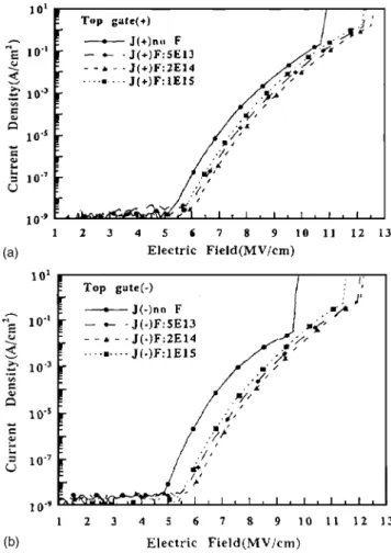
The SIMS profiles of fluorine for the devices implanted with 5⫻ 1013, 2⫻ 1014, 1⫻ 1015F+/cm2and without fluorine implan-tation followed by annealing at 900°C in N2ambient are shown in Fig. 1. Most of the fluorine accumulated within the polyoxide, and the higher the fluorine dose, the higher the fluorine peak value. There are also some amounts of fluorine existing, especially within the bottom polysilicon. A set of the typical J-E characteristics of nonimplanted and fluorine-implanted polyoxides is shown in Fig. 2a and b, respectively. It is clear that all the fluorine-implanted polyox-ides have lower leakage currents and higher breakdown electric fields than those of the nonimplanted polyoxide for both cases of positive gate bias 共electron injection from the bottom polysilicon interface兲 and negative gate bias 共electron injection from the top polysilicon interface兲. The improvements of the electrical character-istics are believed to be due to the fact that the implanted fluorines can passivate the dangling bonds and break the strained Si–O–Si bonds to form Si–F bonds in the polysilicon grain boundaries and polyoxide/polysilicon interface.16,28,20So, the local stress can be re-*Electrochemical Society Active Member.
z
E-mail: [email protected]
Journal of The Electrochemical Society, 154共4兲 H259-H262 共2007兲
0013-4651/2007/154共4兲/H259/4/$20.00 © The Electrochemical Society H259
) unless CC License in place (see abstract). ecsdl.org/site/terms_use
address. Redistribution subject to ECS terms of use (see 140.113.38.11
laxed in the oxide network and make the polysilicon/polyoxide in-terface morphology smoother. Because the stress between the poly-oxide and the polysilicon affects the polypoly-oxide breakdown strength, the lower the oxide stress, the higher the oxide breakdown strength.29
In this experiment, we found that the optimum dose of fluorine to obtain the best polyoxide J-E characteristics is 2⫻ 1014cm−2. But too much fluorine共1 ⫻ 1015cm−2兲 seems to cause degradation of the polyoxide characteristics. The degradation observed for the high-est implanted共1 ⫻ 1015cm−2兲 sample could be due to higher im-plantation damage in bottom polysilicon at a higher dose, and during annealing defect distribution can cause degradation in oxide charac-teristics. Besides, Nishioka et al.30have reported that excessive fluo-rination may result in a high density of nonbridging oxygen centers to induce performance degradation through the O displacement by F from strained Si–O–Si bonds, despite accompanying a local strain relaxation which suppresses the defect migration. However, it still had better characteristics than that of the nonimplanted sample. Figure 3a-c shows the AFM images of bottom polysilicon surface for nonimplanted and 2⫻ 1014, 1⫻ 1015fluorine/cm2 implanted samples, and the average roughness共Ra兲 values of AFM are 58, 35, and 32 Å, respectively. It is clearly seen that the fluorine-implanted samples had more smooth surfaces than that of the nonimplanted sample. This is due to the incorporated fluorine breaking the strain bonds to form stronger Si–F bonds in the interface, thereby making the surface morphology smoother. Although the 1⫻ 1015dosage sample had similar surface morphology as 2⫻ 1014dosage sample, too much fluorine共1 ⫻ 1015兲 still results in inferior characteristics as shown in Fig. 2.
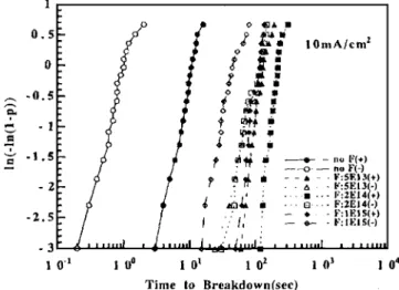
The fluorine-implanted polyoxides also exhibit larger reliability improvement. The charge trapping characteristics of the fluorine-implanted polyoxides were investigated. Figure 4 shows the curves of gate voltage shift共⌬Vg兲 vs time of the polyoxides without and
with different dosages of fluorine implantation under a constant ±100A/cm2 current stressing. The test capacitor area was 5⫻ 10−4cm2. All the increase in the gate voltage is due to electron trappings. All the fluorine-implanted samples had smaller voltage shifts than the nonimplanted sample under the positive and negative current stresses. This means that the fluorine can passivate or reduce the generated traps and defects by the dangling and strain bonds in the polyoxide/polysilicon interface and grain boundaries, so the fluorine-implanted polyoxides trap fewer electrons than the nonim-planted polyoxide.31The optimum dose of fluorine共2 ⫻ 1014兲 also had the best trapping characteristics for both direction current stresses. In nonvolatile memory cells, the charge-to-breakdown 共Qbd兲 is also a critical parameter of interest. Figure 5 shows the
Weibull charge-to-breakdown共Qbd兲 plot for the polyoxides without
and with different fluorine doses implantation under ±10 mA/cm2 stress. The fluorine-implanted polyoxides had larger Qbdwith nar-rower Qbd distribution than those of the nonimplanted polyoxide.
This should be due to the reduced electron trapping shown in Fig.4. The values of the charge-to-breakdown 共Qbd兲 under the positive stress were larger than those under the negative stress for all the polyoxides. Moreover, the Qbd improvement of the fluorine-implanted polyoxide is apparent for the +Vgstress. This is also due
to the incorporated fluorine breaking the strain bonds to form more strong Si–F bonds in the interface, thereby making the surface mor-phology smoother to reduce electron trapping rate. The fluorine im-planted dose 共2 ⫻ 1014cm−2兲 of polyoxide has the largest
Qbd 共⬃2 C/cm2兲 for the +Vg stress. However, excess amount of
fluorine共1 ⫻ 1015cm−2兲 seemed to reduce the Q
bdimprovement. Conclusion
In conclusion, the above results show that the incorporation of fluorine in the polyoxide not only improves the electrical character-istics共i.e., lower leakage current, higher electrical breakdown field兲, but also improves the reliability共lower electron trapping rate, larger
Qbd兲. This improvement is believed to be due to the stress relaxation
of the polyoxide and smoother polysilicon/polyoxide interface by the fluorine incorporation. The optimum fluorine dose 共2 ⫻ 1014兲 shows the best characteristics such as Ebd over 12 MV/cm and
Qbd⬃ 2 C/cm2. However, excessive fluorination共1 ⫻ 1015兲 seems to result in performance degradation due to the generation of non-bridging oxygen centers.
Figure 1. The SIMS profiles of fluorine for the devices implanted with
5⫻ 1013, 2⫻ 1014, 1⫻ 1015F+/cm2and without fluorine implantation,
re-spectively.
Figure 2. The J-E characteristics of the polyoxides implanted with different
doses of fluorine under共a兲 the positive gate bias, and 共b兲 the negative gate bias.
H260 Journal of The Electrochemical Society, 154共4兲 H259-H262 共2007兲
H260
) unless CC License in place (see abstract). ecsdl.org/site/terms_use
address. Redistribution subject to ECS terms of use (see 140.113.38.11
Chang Gung University assisted in meeting the publication costs of this article.
References
1. Y. Nishioka, E. F. da Silva, Jr., Y. Wang, and T. P. Ma, IEEE Electron Device Lett., 9, 38共1988兲.
2. Y. Nishioka, Y. Ohji, K. Mukai, T. Sugano, Y. Wang, and T. P. Ma, Appl. Phys.
Lett., 54, 1127共1989兲.
3. Y. Mitani, H. Satake, Y. Nakasaki, and A. Toriumi, IEEE Electron Device Lett., 50, 2221共2003兲.
4. T. B. Hook, E. Adler, F. Guarin, J. Lukaitis, N. Rovedo, and K. Schruefer, IEEE
Electron Device Lett., 48, 1346共2001兲.
5. P. J. Wright, M. Wong, and K. Saraswat, Tech. Dig. - Int. Electron Devices Meet., 1987, 574.
6. P. J. Wright and K. Saraswat, IEEE Electron Device Lett., 36, 879,共1989兲. 7. K. K. Bourdelle, H.-J. L. Gossmann, S. Chaudhry, and A. Agarwal, IEEE Electron
Device Lett., 22, 284共2001兲.
8. G. Q. Lo, W. Ting, J. H. Ahn, D. L. Kwong, and J. Kuehne, IEEE Electron Device
Lett., 39, 148共1992兲.
9. P. J. Wright, N. Kasai, S. Inoue, and K. Saraswat, IEEE Electron Device Lett., 10, 347共1989兲.
10. J. Ahn, G. Q. Lo, W. Ting, D L. Kwong, J. Kuehne, and C. Magee, Appl. Phys.
Lett., 58, 425共1991兲.
Figure 3. The AFM images of bottom polysilicon surface for共a兲 nonimplanted, 共b兲 2 ⫻ 1014, and共c兲 1 ⫻ 1015F+/cm2implanted samples, respectively.
Figure 4. The curves of gate voltage shift共⌬Vg兲 vs time of the polyoxides
without and with different dosages of fluorine implantation under a constant ±100A/cm2current stressing.
Figure 5. The Weibull charge-to-breakdown plots for the implanted
polyox-ides and nonimplanted polyoxide devices under both positive and negative current stress. A constant current density of 10 mA/cm2was applied to
ca-pacitors with an area of 5⫻ 10−4cm2.
H261
Journal of The Electrochemical Society, 154共4兲 H259-H262 共2007兲 H261
) unless CC License in place (see abstract). ecsdl.org/site/terms_use
address. Redistribution subject to ECS terms of use (see 140.113.38.11
11. Y. Nishioka, K. Ohyu, Y. Ohji, and T. P. Ma, IEEE Electron Device Lett., 10, 540 共1989兲.
12. A. Halimaoui, D. Lenoble, A. Grouillet, J. Weeman, Z. Fang, and S. Mehta, in
IEEE Device Research Conference, Santa Barbara, CA, 1990.
13. E. F. da Silva, Jr., Y. Nishioka, and T. P. Ma, Tech. Dig. - Int. Electron Devices
Meet., 1987, 848.
14. E.F. da Silva, Jr., Y. Nishioka, and T. P. Ma, IEEE Trans. Nucl. Sci., NS-34, 1190 共1987兲.
15. T. P. Ma, Mater. Res. Soc. Symp. Proc., 262, 741共1992兲.
16. D. N. Kouvatsos, F. A. Stevie, and R. J. Jaccodine, J. Electrochem. Soc., 140, 1160 共1993兲.
17. H. N. Chern, C. L. Lee, and T. F. Lei, IEEE Electron Device Lett., 15, 181共1994兲. 18. S. Maegawa, T. Ipposhi, S. Maeda, H. Nishimura, T. Ichiki, M. Ashida, O. Tanina, Y. Inoue, T. Nishimura, and N. Tsubouchi, IEEE Trans. Electron Devices, 42, 1106 共1995兲.
19. K. W. Kim, K. S. Cho, J. I. Ryu, K. H. Yoo, and J. Jang, IEEE Electron Device
Lett., 21, 301共2000兲.
20. H. N. Chern, C. L. Lee, and T. F. Lei, IEEE Trans. Electron Devices, 41, 698 共1994兲.
21. S. De Wang, T. Y. Chang, C. H. Chien, W. H. Lo, J. Y. Sang, J. W. Lee, and T. F. Lei, IEEE Electron Device Lett., 26, 467共2005兲.
22. M. K. Hatalis, J. H. Kung, J. Kanicki, and A. A. Bright, Mater. Res. Soc. Symp.
Proc., 182, 357共1990兲.
23. S. Mori, Y. Kaneko, N. Arai, Y. Ohshima, H. Araki, K. Narita, E. Sakageminand, and K. Yoshikawa, in Proceedings 28th IRPS, pp. 132–144共1990兲.
24. M. Hendriks and C. Mavero, J. Electrochem. Soc., 138, 1466共1991兲.
25. L. Faraone, R. Vibronek, and J. McGinn, IEEE Trans. Electron Devices, ED-32, 577共1985兲.
26. A. Shintani and H. Nakashima, Appl. Phys. Lett., 36, 983共1980兲. 27. M. C. Jun, Y. S. Kim, and M. K. Han, Appl. Phys. Lett., 66, 2206共1995兲. 28. D. Kouvatsos, J. G. Huang, and R. J. Jaccodine, J. Electrochem. Soc., 138, 1752
共1991兲.
29. R. J. Mattauch and W. H. Howle, IEEE J. Solid-State Circuits, 11, 732共1995兲. 30. Y. Nishioka, K. Ohyu, Y. Ohji, N. Natuaki, K. Mukai, and T. P. Ma, IEEE Electron
Device Lett., 10, 141共1989兲.
31. H. Kitajima, Y. Suzki, and S. Saito, in Extended Abstracts of SSDM, 1991, pp. 174–176.
H262 Journal of The Electrochemical Society, 154共4兲 H259-H262 共2007兲
H262
) unless CC License in place (see abstract). ecsdl.org/site/terms_use
address. Redistribution subject to ECS terms of use (see 140.113.38.11