Characteristics of Top-Gate Polysilicon Thin-Film Transistors
Fabricated on Fluorine-Implanted and Crystallized
Amorphous Silicon Films
Chien Kuo Yang, Tan Fu Lei, and Chung LenLeeDepartmentof Electronics Engineering, National Chiao Tang University, Hsinchu, Taiwan ABSTRACT
This paper presents a comprehensive study on the characteristics of n- and p-channel polycrystalline—silicon
(poly-silicon) thin-film transistors (TFTs) fabricated on fluorine-implanted-then-crystallized amorphous silicon films.
Amorphous silicon films of two thicknesses were implanted with different energies and various dosages of fluorine, and studied using transmission electron microscopy (TEM) and secondary-ion mass spectrometry (SIMS). The electrical char-acteristics of TFTs fabricated on the films were correlated with the results of TEM and SIMS. It was found that field-effect mobilities of both n- and p-channel devices were improved by the fluorine implantation thanks to the enhanced grain size and the fluorine passivation effect. For the p-channel device, the fluorine implantation did not improve the sub-threshold swing and even degraded it after hydrogenation. This result was thought to be caused by the fluorine-induced negative charges in oxides. However, a thin active layer and a deep implantation reduced this degradation.
In 1980 Kanrins et al.1 were the first to suggest that flu-orine be used to passivate grain boundaries of the polysil-icon TFT. The concept was not realized until 1991,
howev-er, when fluorine ion implantation (FlI) was used to
incorporate fluorine into the poly-Si TFT2 and studies indicated an improvement in device performance.Re-cently, other studies have further examined the effects of FIT on the polysilicon TFT.35 For example, Chern et al.1 studied the passivation effects of fluorine on polysilicon thin-film transistors by implanting different doses of flu-orine into the device channel. Generally, FIT was applied
to the polysilicon TFT in two ways, i.e., fluorine was
implanted after the amorphous-silicon (a-Si) crystalliza-tion,3'4 or before the a-Si crystallization.5 For Fli applied after the a-Si crystallization, the fluorine had demonstra-ble passivation effects on the polysilicon TFT to improve device performance.1-3 Moreover, because of the fluorine incorporation, negative charges were induced in the oxide under the offset region of the bottom-gate TFT, creating an LDD-like structure to further improve the TFTs ON- and OFF-currents.4 In the above reports on FIT applied after
the a-Si crystallization, the grain regrowth effect of the amorphized film was not considered, even though high implantation doses and energies were used.6 A recent
study on FIT before the a-Si crystallization reported that
fluorine implantation with high doses and deep
projec-tion-ranges, like silicon implantation, could also enhance the grain sizes of, but have no passivation effects on, the polysilicon.1 The same study also reported that fluorine was a hole generator in the recrystallized polysilicon films. However, this study5 showed inconsistent results between
material properties and electrical characteristics (e.g., a
larger grain-size TFT but a lower ON-current), and
elec-trical characteristics were not characterized completely
(e.g., without p-channel devices).
In this work, FIT applied to as-deposited a-Si films to fabricate TFTs was thoroughly studied. Fluorine of
differ-ent doses and energies were implanted into a-Si of two
thicknesses, n- and p-channel polysilicon TFTs were fab-ricated, and their electrical properties were discussed in detail. At the same time, the hydrogen passivation effect
on the fabricated TFTs was also studied. Transmission
electron microscopy (TEM) and secondary-ion mass spec-trometry (SIMS) were used to investigate the implanted a-Si which received different thermal treatments, includ-ing low-temperature (550°C) crystallization and
high-tem-perature (850°C) oxidation and annealing. It was found
that the improved electrical characteristics could be
attributed to both the enhanced grain size by FIl and the fluorine's own passivation effect. Moreover, the fluorine-induced negative charges in oxides were thought to be thereason for the degradation of the p-channel device's sub-threshold swing.
Experimental
At first, undoped a-Si films of two thicknesses, approx-imately 100 and 60 nm, were deposited on thermally oxi-dized silicon wafers at 550°C by a low-pressure chemical vapor deposition (LPCVD) system. These films were then implanted by fluorine. For the thicker films, the
implanta-tion energy was 30 key and the dose varied from 8 >< 1014 cm2 to 3 X 1015 cm1. For the thinner films, the
implantation energies were 5, 15, and 30 keV with a dose
of 2 >< 1011 cm2. These wafers were then annealed at 600°C for 45 h to transform the a-Si films into polycrystalline films. After active islands were defined, a 28 nm gate oxide was grown in dry 02 at 850°C. Another 300 nm
poly-silicon film was deposited at 625°C by the LPCVD system to be the gate electrode. Self-aligned As and BF2 implan-tations of a dose of 5 x
10
cm1 were performed to formthe source and the drain and to dope the gate electrodes
for the n- and p-channel devices, respectively. The implan-tation energies are 65 and 40 key for 100 and 60 nm poly-silicon films, respectively. The dopants were activated at 850°C for 30 mm in an N3 ambient. Some samples were subjected to the H2/N2 plasma treatment in a commercial
plasma-enhanced chemical vapor deposition (PECVD)
system at 300°C for 1 h. All devices were then capped with a 360 nm PECVD 5i02. The total pressure was 800 mTorr,
the RF power was 10 W, and the deposition rate was
60 nm/mm. Finally, after contact holes were opened, Al
was deposited, patterned, and then sintered at 300°C.
During the above process, control devices without the flu-orine implantation were also fabricated for comparison. All the devices, with and without the fluorine implanta-tion, were pretreated by a diluted HF solution without a
water rinse and immediately spun dry just before their
gate-oxide growth. The diluted HF treatment was denoted as DHF
Resultsand Discussion
100mm poly-si film devices—Figure la and b shows the
TEM micrographs, including the diffraction patterns and the dark-field images, of the poly-Si films without FIT,
and with 3 >< 1011 cm2 FIl, respectively. The grain size of
the FIl film was effectively enhanced as compared to the unimplanted film. The diffraction pattern of the ElI film
also shows how the FIl film had crystallized more than
the film without FIl. This contradicts the report by Park et al.,1 which showed no increase of the grain size of the poly-Si film, even when the fluorine implantation exceed-ed 5 X 1011 cm2.
Fig.1. The TEM micrographs, including diffraciion pattern and
dark-field image, of the samples with (a) no FlI and (b) 3 x
10's cm2 FlI.
Figure2 shows the SIMS data on the fluorine
distribu-tions of the films with 1 x 1O' and 3 x io' F/cm2 implan-tations, respectively. The implanted fluorine, after the
fol-lowing annealing and oxidation steps, had redistributed itself into the gate- and isolation-oxides, with most of
them gathering at gate-oxide/poly-Si/S102 interfaces. The original implanted fluorine peak disappeared and the 3 x
10"cm2 film had higher fluorine peaks at interfaces, yet
it had the same distribution as that of the 1 x10"cm2
film at the polysilicon bulk.
10
10'
250 300 350 400 450
Depth (nm)
Fig. 2. The SIMS profiles of the samples with 1 x 1O and 3 x
10" F/cm2 implantations, respectively.
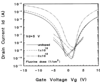
Figure 3 shows the drain currents, before hydrogen
pas-sivation, as a function of the gate voltage of n- and
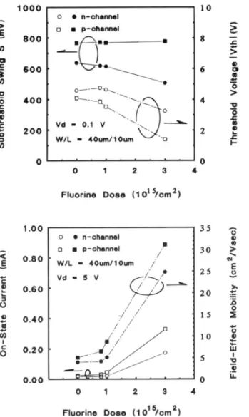
p-channel TFTs fabricated on poly-Si films with various Fil doses. Figure 4a and b shows the values of the electrical parameter of the ON-state current, the field effect mobili-ty, the subthreshold swing, and the threshold voltage
plot-ted as a function of the implantation dose, for n- and p-channel TF'Ts, respectively. These figures show that, (i) Fil
improved the device characteristics for both the n- and p-channel TFTs and (ii) the greater the implanted dose, the
greater the improvement, except for the OFF-state
cur-rent. The improvement was not significant, however, until the dose was increased to at least 3 X lO"cm'. Also, com-pared with the n-channel devices, the p-channel devices
had different subthreshold characteristics. Obviously it was the grain-size enhancement, caused by the fluorine implantation, that improved the device characteristics. However, in addition to that, some other mechanisms
could also have played roles in affecting the device char-acteristics; examples could be the enhanced OFF current
or the different subthreshold characteristics between
n-and p-channel devices. One such mechanism could be that fluorine acted as a hole generator in recrystallized polysil-icon films because of its large electron-negativity,'' which would lead to p-channel devices being in the accumulation mode and n-channel devices in the inversion-mode." This made p-channel devices switch on more easily than did n-channel devices. Nevertheless, in Fig. 2, it was observed
that more fluorine accumulated at the Si/SiO2 interface than at the bulk of poly-Si. It is believed that it was the fluorine at the Si/5i02 interface, rather than at the
poly-silicon bulk, that increased the OFF-state current. Hence, another possible mechanism considered was the double-gate effect caused by the negative fixed charges induced by fluorine incorporated in oxides.12 The negative fixed oxide charges caused positive flatband shifts. Therefore,
for the top-gate, the turn-on voltage of the top channel
was shifted to the positive. In addition, an induced
back-channel caused by the negative charges in the isolation
oxide occurred. This affected both the drain leakage cur-rent and the subthreshold characteristic.'3'4 For n-channel
Fil devices, the enhanced negative bias on the top-gate
and the additional negative bias on the bottom-gate
increased the electrical field at the drain junction; this increased field in turn led to the increased anomalousleakage current. The drain junction leakage was the main source of the anomalous leakage current, i.e. the OFF cur-rent, for TFTs." For p-channel Fli devices, due to the
neg-ative charges, the top and back channel might be still
slightly ON until the top-gate bias is positive enough.
.-.-. ..—
.—
/Z
Vd-5 V
(
Fluorin. do.. (1/am2)
-15 —10 —5 0 5 10
Gate Voltage Vg (V)
Fig. 3. The drain current, before hydrogen passivation, as a func-tion of gate voltage for the devices with various Fil doses.
10'
10'
10' 10' 10' 10$ 4-C0
0
4, C5-0
IL 'C 4-C 4,I-0
C5-a
10'
I0'
10'
10'
10 -Y10•
10'
10-'• 10-I'The above leakage current can be reduced effectively if a thinner polysilicon film is used; this issue is discussed
later.
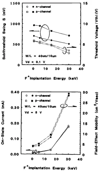
60 nm poly-Si film devices—Figure 5 shows TEM
micrographs, including diffraction patterns and dark-field
images, for samples without Fil (a) and implanted with fluorine at 15 (b) and 30 keV (c). The dosage of FlI was 2 x
10
cm2and the film thickness was 60 nm. For samples implanted at 15 keV and having the projected implanta-tion range of about 30 nm, the grain size was only slightly than that of the control sample. However, for the 30 keVsample, with the projected implantation range slightly larger than 60 nm, the grain size was much enhanced.
These results are similar to those reported by Park et al.5
Hence, in order to increase the recrystallized grain size
effectively, the implantation range should fall at the inter-face of the poly-Si film and the bottom isolation oxide. In addition, the grain size of the 30 keV sample in this section
was smaller than that of the sample in Fig. 1. This was
mainly because the 30 keV sample had a thinner poly-Si film which limited grain-growth.
Figure 6a-c shows the fluorine distributions of samples with three different implantation energies, i.e., 5, 15, and 30 keV, respectively, and the distributions of the control
sample which did not receive any FIT but still received
diluted HF (DHF) acid treatment. For these three implan-tation energies, the projected implanimplan-tation peaks were at the top, the middle, and the bottom of the poly-Si films,
Fig. 5. The TEM micrographs, including diffraction pattern and dark-field image, of the samples with different implantation
ener-gies: (a) control, (b) 15 keV, and (c) 30 keV.
respectively.Due to the subsequent annealing and
oxida-tion processes, most of the fluorine redistributed itself into the gate- and isolation-oxides or on the curves, and so the original peaks did not exist. However, the larger the im-plantation energy, the higher the fluorine peak at the
bot-tom poly-Si/Si02 interface. Likewise the DHF control
sample had a peak at the gate-oxide and the 5 keV sample
gave a similar fluorine distribution near the
gate-oxide/poly-Si interface as compared to the DHF control sample. This indicates that the DHF treatment also incor-porated a significant amount of fluorine into its devices.
Figure 7 shows the drain current, before hydrogen pas-sivation, as a function of the gate voltage for devices with
various FIT energies. Interestingly, I-V improvements were
obtained by FII, even for the 5 keV sample. This contrasts
reports from Park et al.,5 where Fli did not effectively improve I-V. The 30 keV device had the best electrical
characteristics due to its largest grain size; its only flaw
was a slightly increased OFF-state current. The slightly
increased OFF-state current, similar to that of the 100 nm
device, probably came from the many fluorine-induced
3304 J. Electrochem. Soc., Vol. 143, No. 10, October 1996 The Electrochemical Society, Inc. 10 8 o • n-Channel o U p-channel 6 800 600 400 200 0 0 1 2 3 Fluorine Dose (101 51cm2) 4 2
>
E 0) C U, 0 S V I-.0 CO 'C E C I-C) V a U) C0
0>
>
V C 0>
0 0 V I-I-.35
-V S30
25 20 .0 0 15I
1.00 0.80 0.60 0.40 0.20 0.00 0 1 2 3 4 Fluorine Dose (101 51cm2)Fig. 4. The electrical parameters, including (a, top) subthreshold
swing and threshold voltage and (b, bottom) field-effect mobility
—:3OkeV
15 key S key 2x101 F/cm2 2x101 F/cm2 2x10 F/cm2lot
10'
10
10'
I
c-si
'V 4S C0
C) a, CI-0
LLcharacteristic improvement was minimal and indeed
almost the same as that of the control sample.
Figure 8a shows the parameter values of the ON-state current and field-effect mobility while Fig. 8b gives the subthreshold swing and threshold voltage: all four values are expressed as a function of the implantation energy for
the corresponding devices of Fig. 7. All cases demonstrated that the higher the implantation energy, the greater the
improvement of the driving ability, the threshold voltage, and the subthreshold swing. Figure 8b clearly shows that
the improvements on subthreshold swings of n- and p-channel devices were similar. This differed from that of the
100rimdevices of the first section, where improvement for the 3 )< 1015cm2 p-channel device was not obtained.
Because the 60 nm device was fabricated on thinner poly-silicon layer, its subthreshold characteristic could be more
effectively controlled by the top gate and the OFF-state
cur-rent was reduced despite the existence of the induced back channel.13
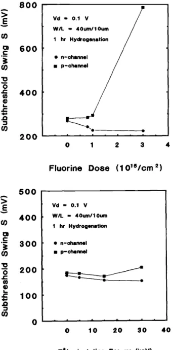
Hydrogen passivation effect—Figure 9 shows the sub-threshold-swings as a function of (a) the fluorine dose for 100 nm poly-Si film devices and (b) the implantation ener-gy for 60 nm poly-Si film devices after hydrogen passiva-tion. Comparing the data in Fig. 9, 4b, and 8b showed that hydrogen passivation improved the subthreshold swings of all devices except for the 100 nm sample implanted with a dose of 3 x1015cm2 at 30 keV in Fig. 9a. Figure 9a
mdi-15 a, C 0 C Polysilicon Charnel
10'
-10 0
10 20 30 40 50
Depth (nm)
Fig. 6. The SIMS profiles of the samples with different implanta-tion energies and the control without Fli.
chargesin the oxides. However, compared to the 100 nm
device, the 30 keV device's leakage-current was lower due to the smaller thickness of the active layer.15 As for the 15 keV device, although its grain size was not increased significantly, it still apparently improved electrical
prop-erties. This improvement is believed to stem from the
com-bination of the grain size effect and the passivation effect of fluorine which resided in the film after crystallization.
Park et at.5 reported that although Fil significantly
enlarged grain size, little I-V improvement was found even for the sample implanted with fluorine at a high dose (4 )<iO cm2) and a high implantation energy (60 keV). The 5 keV device was quite different, however: since the implantation damage was not severe and the implanted
fluorine outdiffused during the crystallization stage, the
o • n—channel o • p-channel W/L — 4Oum/lOum Vd — 0.1 V
>
E 0)a
C 030
0 S a, I-S. .0 03I'
£1
C 4 6. I-C 4, S. S 4-C0
1500
1000500
00.40
030
0.20 0.10 0.00 0 10 20 30F4 Implantation Energy (keV)
4< .5 4.. C 4) I-6. C) C C 6.
0
>4 S. >4 10 a C 4-0 >4V
5 0 C 4, 6.I--0
40 30 a,S
>4 25 £ C,20
— S. 15 S.' 0
V S 10-' 10-s 10-' 10-s 10-' 10-' 10-' 10-Is 10-I' undoped 5 (cv —--—-15 Ktv —-—-—30 Key Dose 2x10¹⁵ FIcm2 —15 -10 -5 0 S 10Gate Voltage V9 (V)
Fig. 7. The drain current, beforehydrogenpassivation, as a func-tion of gate voltage for the devices with various FIl energies.
0
0 10 20
30 40
F lmplantation Energy (key)
Fig. 8. The electrical parameters, including (a, top) subthreshold
swing and threshold voltage, and (b, bottom) field-effect mobility and ON-state current as a function of implantation energy for the
3306 J. Electrochem. Soc., Vol. 143, No. 10, October 1996 The Electrochemical Society, Inc.
Fig. 9. The subthreshold-swing (5), after hydrogen passivation, as
a function of (a, top) fluorine dose and (b, bottom) implantation energ respectively.
cates that after hydrogen passivation the
subthreshold-swing of the p-channel device was degraded, especially for the 3 x 10" cm' case, as the fluorine dose increased. For
the n-channel device, however, the subthreshold swing was improved further. These results could also be
ex-plained by the fluorine-induced negative charges at the
isolation oxide (i.e., bottom oxide). After hydrogen passi-vation, and because the trap-states were reduced more, the bottom channel, induced by the fluorine-induced negative charges, conducted more easily for the p-channel devices. The conducting back-channel made top-gate control of the drain-current less effective at the low top-gate bias, espe-cially for the device with a thick active layer,13 and then led to the increased of both the S factor and the OFF-state current. Thinning the active layer increased the
controlla-bility of the top-gate to the whole active layer and
sup-pressed the back-channel effect. This explains why the 5-factor of the 30 key p-channel device of the 60 nm sample in Fig. Qb was not so seriously degraded as that of the 100 nm p-channel device in Fig. 9a. Another possible reason was that the 30 keV FIT had more seriously damaged the bottom poly-Si/SiO2 interface of the thin-film device. The damage could reduce the hole life time at the bottom sur-face,16 so the back-channel did not conduct well.
The field-effect mobilities of the devices in Fig. 9, where
they were hydrogen-passivation treated, are summarized in Table I with their process condition. For comparison,
the mobilities of devices of a previous work3 are also included. It is seen that hydrogen passivation further
enhanced the field-effect mobilities of both the n- and p-channel devices. The DHF treatment, applied after
crys-tallization but before gate-oxidation, gave field-effect
mobilities comparable with those of the
fluorine-implant-ed devices of 2 x10"cm'at 25 keV, and annealed at 850°C for 1 h.
Conclusions
This study systematically examined FIT prior to a-Si
crystallization and its effects on the TF'Th fabricated on the FIT poly-Si thin films. FIT prior to a-Si crystallization improved the electrical characteristics of the TFT, with the improvement coming from both the grain size enhance-ment and the fluorine passivation effect. The higher the implantation dosage and energy, the greater the
ment. As hydrogenation was applied, further improve-ments on electrical characteristics, especially in
field-effect mobility, were found. There was a negative charge effect, however, which was induced by the implanted flu-orine at the gate as well as at the bottom oxides and which affected device characteristics, such as S and OFF-state current. This negative charge effect increased the
p-chan-nel TFT leakage and degraded S after hydrogenation.
However, this condition could be reduced if the thickness of the active poly-Si film was decreased. Finally, it was found that applying the DHF process to the poly-Si film before it was subjected to gate oxidation introduced fluo-rine into TF'Th to obtain the desired passivation effect.
Acknowledgment
This work was supported by the ROC National Science Council under Contract No. NSC-83-0404-E009-017.
Manuscript submitted Sept. 14, 1995; revised
manu-scripot received July 1, 1996.
The National Chiao Tung University assisted in meeting the publication costs of this article.
Table I. Summary of process conditions and field-effect mobilities after hydrogen passivation in this work and a previous report by Chern at c,!.3
p. (cm'/Vs)
Polysilicon Preimplantation Fluonne ion Anneal or
thickness preparation of films implantation crystallization DHF n-channel p-channel
60 oin° 550°C a-Si, 600°C 20 h — — No 12.0 10.8 60 nin° 550°C a-Si, 600°C 20 h 2 X 1013cm'25 keV 850°C 1 h No 20.2 14.6 100 rim 550°C a-Si, — — 600°C45 h Yes 18.0 16.4 100 nm 550°C a-Si, — 3X 10" cm' 30 keV 600°C 45 h Yes 41.7 44.0
600°C45h Yes 20.1 12.8
60mri 550°Ca-Si,—-- —
60nm 550°C a-Si, — 2)<10"cm' 30 keV 600°C 45 h Yes 44.4
34.4 a SeeRef. 3.
>
E U)0
CI
C00
.C tO a) I--c .0 U)>
E U)0
CI
U) -50
.c
0, 4)L -Ca,
.0
U)800
600
400
200
500
400
300
200
100
0
0
12
34
Fluorine Dose (1 0'6Icm 2)
Vd — 0.1 V W/l. — 4Oum/lOum 1 hr Hydrogenation • n—channel • p-charnel
0
10
20
30
40
REFERENCES
1. T. I. Kamins and Marcoux, IEEE Electron Device Letters, EDL-1, 159 (1980).
2. H. Kitajima, Y. Suzuki, and S. Saito, Tech. Dig. Solid
State Dev. Mater., 174 (1991),
3. H. N. Chern, C. L. Lee, and T. F. Lei, IEEE Trans. Electron Devices, ED-41,698 (1994).
4. 5. Maegawa, T. Ipposhi, S. Maeda, H. Nishimura, T.
Ichiki, M. Ashida, 0. Tanina, V. Inoue, T. Nishimura,
and N. Tsubouchi, ibid., ED-42,1106(1995). 5. J. W. Park, D. G. Moon, B. T. Aim, and H. B. Im, Thin
Solid Films, 245, 228 (1994).
6. N. Yamauchi and R. Reif, J. Appi. Phys., 75, 3235 (1994).
7. M. Y. Tsai and B. G. Streetman, ibid., 50, 183 (1979).
8. I. W. Wu, A. Chiang, M. Fuse, L. Ovecoglu, and T. V.
Huang, ibid., 65, 4037 (1989).
9. C. G. van de Walle, F. R. McFeely, and S. T. Pantelides, Phys. Rev, Lett., 61, 1867 (1988).
10. 5. D. S. Maihi, H. Shichijo, S. K. Banerjee, R. Sun-daresan, M. Elahy, G. P. Pollack, W. F. Richardson, A. H. Shah, L. R. Hite, R. H. Womack, P. K. Chat-terjee,andH. W. Lan, IEEE Trans. Electron Devices,
ED-32,258(1985).
11. lvi. Y. Tsai, D. S. Day, B. G. Streetnian, P. Williams, and C. A. Evans, Jr., J. Appi. Phys., 50, 188 (1979).
12. P. J. Wright and K. C. Saraswat, IEEE Trans. Electron
Devices, ED-36, 879 (1989).
13. T. Hashimoto, T. Mine, T. Yamanaka, N. Hashimoto, A.
Shimizu, T. Nishida, and Y. Kawamoto, Tech. Dig.
Solid State Dev. Mater., 393 (1990).
14. F. Hayashi, H. Ikeuchi, M. Kitakata, and I. Sasaki, IEDM Tech. Dig., 501 (1993).
15. J. G. Fossum, A. Ortiz-Conde, H. Shichijo, and S. K.
Banerjee, IEEE Trans. Electron Devices, ED-32, 1878 (1985).
16. K. Fuse, Y. Sakata, T. Inoue, K. Yamauchi, and Y.
Yatsuda, Springer Proceedings in Physics, Vol. 35,
p.370(1989).
The Effect of Post-Cure Annealing on the Protective Properties
of Polyimides on Chromium Substrates
D. B. Milton and R. M. Latanision
H. H. Uhlig Corrosion Laboratory, Massachusetts Institute of Technology, Cambridge, Massachusetts, 02139 USA
F. Bellucci*
Department of Materials and Production Engineering, University of Naples Federico II,
P Le Tecchio 80125,Naples,Italy
ABSTRACT
The effectof post-cure annealing on theprotectiveproperties of thin (2.6-2.8 jim) polyimide films on chromium
metallic substrates was investigated in aerated neutral 0.05, 0.5, and 5 M aqueous NaCl solutions at ambient temperature ("20°C). The study was carried out using the technique of electrochemical impedance spectroscopy to monitor film degra-dation as a function of immersion time in the test solutions. Results obtained indicate that when exposed to aqueous NaC1 solutions for extended periods, a majority of the nonannealed coated substrates failed; however, the performance of the annealed samples was significantly better. At face value, these results suggested improved protective properties of the polyimide due to annealing. However, a more in-depth analysis of the data revealed that post-cure annealing leads to the
development of a thicker oxide on the chromium substrate. The change in the oxide occurring during the post-cure
annealing treatment contributes to the improved corrosion resistance of the polyimide/Cr system.
Introduction
Toimprove signal propagation speed and memory
per-formance in microprocessors, device feature sizes in inte-grated circuits must be reduced to facilitate densification of microelectronics packages. Exposing such systems to aggressive processing and service environments can pose serious corrosion and reliability problems. Therefore, to ensure prolonged performance life and reliability, stringent demands are placed on packaging materials. Although the ability to planarize substrate surfaces, thermal stability,
chemical resistance, and dielectric properties of
poly-imides favorably meet the requirements of such materials, the critical issue of corrosion protection is less well docu-mented.'' Additionally, polyimides are susceptible to the uptake of water and wet polyimides exhibit higher levels of conductivity than those recorded for the dry polymer.6 Permeation of water and subsequently dissolved oxygen and ionic contaminants can alter mechanical' and electri-cal properties of devices leading to early failure.''
Recently, the protective properties of pyromellitic dian-hydride oxidianiline (PMDA-ODA) polyimide coated on
an Al metallic substrate,' have been investigated. This
paper showed that the time to failure for a 2.4 jim PMDA-ODA polyimide on an aluminum substrate immersed in 0.5 M NaC1 varied between a few days and 90 days. Early
*ElectrochemicalSociety Active Member.
failure of samples has so far been interpreted in terms of defects, or pinholes, in the polymer. Conversely, failure observed after extended exposure to the environment was
attributed to the loss of adhesion at the polymer-metal
interface.
To improve the protection of a metallic substrate by a polymer such as polyimide, two aspects should be
consid-ered: (i) improving the adhesion at the polymer-metal
interface and (ii) reducing the preexisting heterogeneities
within the polymer, which may result from unreleased
trapped solvent or unreacted polyamic acid. The first issue
is addressed in this paper by employing a chromium
metallic substrate. It has been demonstrated that adhesion
between polyimide and Cr is better than between poly-hide and other metals such as Al and Cu.' In order to reduce the number of preexisting heterogeneities in the current study, a post-cure anneal was instituted. When
this treatment is carried out at a temperature close to 1's, removal of the residual high boiling point solvents (e.g.,
dimethylacetamide, DMA, and n-methylpyrrolidone, NMP) should reduce the number of preexisting hetero-geneities. In addition, this post-cure thermal treatment will allow the complete curing of unreacted polyimides
which are known to be present in polyimide films and can
be as high as 20%.8
In order to extend our understanding of the protective properties of polyimides, this paper reports an