Atomic-scale epitaxial aluminum film on GaAs substrate
Yen-Ting Fan, Ming-Cheng Lo, Chu-Chun Wu, Peng-Yu Chen, Jenq-Shinn Wu, Chi-Te Liang, and Sheng-Di Lin
Citation: AIP Advances 7, 075213 (2017); doi: 10.1063/1.4991435 View online: http://dx.doi.org/10.1063/1.4991435
View Table of Contents: http://aip.scitation.org/toc/adv/7/7
Published by the American Institute of Physics
Articles you may be interested in
Third nearest neighbor parameterized tight binding model for graphene nano-ribbons
AIP Advances 7, 075212 (2017); 10.1063/1.4994771
Determination of the impact of Bi content on the valence band energy of GaAsBi using x-ray photoelectron spectroscopy
AIP Advances 7, 075016 (2017); 10.1063/1.4986751
Epitaxial nanowire formation in metamorphic GaAs/GaPAs short-period superlattices
AIP Advances 7, 075319 (2017); 10.1063/1.4985550
Behaviors of beryllium compensation doping in InGaAsP grown by gas source molecular beam epitaxy
AIP Advances 7, 075117 (2017); 10.1063/1.4989884
A study of growth and thermal dewetting behavior of ultra-thin gold films using transmission electron microscopy
AIP Advances 7, 075303 (2017); 10.1063/1.4989823
Radio-frequency oxygen-plasma-enhanced pulsed laser deposition of IGZO films
Atomic-scale epitaxial aluminum film on GaAs substrate
Yen-Ting Fan,1Ming-Cheng Lo,1Chu-Chun Wu,1Peng-Yu Chen,1Jenq-Shinn Wu,2Chi-Te Liang,3and Sheng-Di Lin1,a
1Department of Electronics Engineering, National Chiao Tung University, Hsinchu, Taiwan 2Department of Electronic Engineering, National Changhwa University of Education, Changhwa, Taiwan
3Department of Physics, National Taiwan University, Taipei, Taiwan
(Received 20 June 2017; accepted 3 July 2017; published online 24 July 2017)
Atomic-scale metal films exhibit intriguing size-dependent film stability, electrical conductivity, superconductivity, and chemical reactivity. With advancing methods for preparing ultra-thin and atomically smooth metal films, clear evidences of the quantum size effect have been experimentally collected in the past two decades. However, with the problems of small-area fabrication, film oxidation in air, and highly-sensitive interfaces between the metal, substrate, and capping layer, the uses of the quantized metallic films for further ex-situ investigations and applications have been seriously limited. To this end, we develop a large-area fabrication method for continuous atomic-scale aluminum film. The self-limited oxidation of aluminum pro-tects and quantizes the metallic film and enables ex-situ characterizations and device processing in air. Structure analysis and electrical measurements on the prepared films imply the quantum size effect in the atomic-scale aluminum film. Our work opens the way for further physics studies and device applications using the quan-tized electronic states in metals. © 2017 Author(s). All article content, except where
otherwise noted, is licensed under a Creative Commons Attribution (CC BY) license (http://creativecommons.org/licenses/by/4.0/). [http://dx.doi.org/10.1063/1.4991435]
I. INTRODUCTION
High-quality nanoscale metal film is a key element in electronic, plasmonic, and nano-photonics devices and circuits.1,2For example, it has been demonstrated that the crystal quality of metal films plays an essential role in making high definition optical antennas as well as improving the perfor-mance and operating temperature of plasmonic nanolasers.2–5Electrical transport properties can also be enhanced by using high-quality metals owing to the reduced loss,6,7which could benefit the fab-rication of superconducting qubits.1 With film thickness reduced from the nanometer scale to the atomic scale, a metal exhibits intriguing properties, due to so-called quantum size effect, and opens a window for fundamental science exploration and novel device development.8–12Unlike that in semi-conductors, electronic quantum size effect in metals has been much more difficult to be observed because of its extremely short Fermi wavelength (< 1 nm). Driven by the huge potential of the quan-tized electronic/metallic states for various applications, searching for a practical and reliable method for preparing an atomic-scale metal film has been a long-standing challenge for material scientists and engineers.13–21
To prepare an atomically uniform and thin metal film, small area (∼µm2) and low tempera-ture deposition in an ultra-high vacuum (UHV) chamber are commonly applied. Extensively studied metals such as silver and lead reveal quantum size effect on chemical reactivity, film stability, super-conductivity, and electrical super-conductivity, etc.9,14–21To prevent the samples from oxidation, the films were mostly in-situ characterized in a UHV chamber, which makes them almost not possible for practical applications.8,9An over layer on top of the films to avoid oxidation is feasible.21However,
aCorresponding author e-mail address:[email protected]
075213-2 Fan et al. AIP Advances 7, 075213 (2017) 1) the physical properties of the atomic-scale metal film is very sensitive to the over layer and the interface between them, and 2) it is difficult to make good electrical contact without exposing the metal film to the air. As the most abundant metal on earth, aluminum does oxidize in air but its self-limiting oxidation makes it applicable in many circumstances. Although there were theoretical works on the quantum size effect of Al, no clear corresponding ex-situ experimental evidences were reported.9–11In the present work, we use molecular beam epitaxy (MBE) to prepare a large-area, high-quality Al film of atomic-scale thickness. The Al films grown on GaAs (001) substrate were
ex-situ characterized by X-ray diffraction (XRD), atomic force microscopy (AFM), cross-sectional
transmission electron microscopy (TEM), optical reflectivity and four-probe electrical measurements. The continuous Al film of few atomic layers, observed in the cross-sectional TEM images, showing anomalous electrical properties in both normal and superconducting states, which could be explained with quantum size effect. Our work builds a playground for ex-situ studies of the quantum size effect in metals and paves a way for future applications using atomic-scale metal films.
II. SAMPLE GROWTH AND CHARACTERIZATION METHODS
Our samples in this work were prepared in a Varian Gen-II solid-source MBE system.4–6 After native oxide desorption of a semi-insulating GaAs (001) substrate, a 200-nm-thick undoped GaAs buffer layer was grown at 580oC first. The GaAs surface was then heated to 600oC with no arsenic flux for 3 minutes to transform the surface into Ga-rich condition. The treated sample was cooled down in the ultra-high-vacuum chamber to prevent the surface from oxidation. Al growth continued after that the residual arsenic vapor in the chamber was pumped away and the background pressure was less than 2x10⁻¹⁰torr. The growth rate of the Al films was 0.1nm/s. Four samples, named as A, B, C, and D, with respective deposited Al thickness of 3, 5, 10, and 20 nm were prepared. The samples were characterized by the following methods. Cross-sectional TEM samples were prepared by using focused ion beam. Sample size was about 5-7 µm in length and 2-3 µm in depth. AFM measurement was performed in air with the tapping mode in Bruker Edge. Reflectivity spectra were taken by N&K 1500 with the wavelength step of 1 nm. To carry out the electrical measurement, the samples were processed with standard photolithography into a Hall bar with the length of 800 and 1600 µm and the width of 100 µm. Pads with indium solder were wire-bonded to a lead-free ceramic chip carrier for low temperature measurement. A4He cryostat system with the lowest temperature of about 1.4 K and with the highest magnetic field up to 14 T was used for the electrical characterization. Normal-state resistivity was obtained with the current-voltage linear curves measured by four-probe method and a dc source meter, Keithley 2400. The critical field and temperature of superconductivity investigations were performed in the same system with a constant injection current about 10-100 µA.
III. RESULTS AND DISCUSSIONS
Figures1a–1dshow the typical 5 × 5 µm2 AFM top-view images of the four samples in air. Note that the height scale bar ranges from -1 to 1 nm. Smooth surfaces are obtained from all four samples with the root-mean-square (RMS) roughness of 0.28, 0.27, 0.25, and 0.38 nm for samples A, B, C, and D, respectively. Figure2shows the 2θ scanning XRD on sample D (20-nm-thick Al device) measured in the high intensity mode. The XRD shows a weak but clear Al (111) peak at about 38.14°, revealing the crystalline nature of grown Al film. We would like to mention that the XRD on samples A, B, and C were also performed and the Al (111) peaks of sample B and C were weaker and broader but still observable but, for sample A with thinnest Al, the Al XRD signal was too weak to be seen under the available measurement condition.
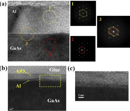
Figure3ashows the cross-sectional high-resolution TEM images taken from sample D. Nearly defect-free Al (upper) and GaAs (lower) layers with a clear and abrupt Al/GaAs interface are observed. The electron diffraction patterns at three regions, Al, GaAs, and the Al/GaAs interface, indicated with the dashed circles are also presented on the right in Figure3a. The clear spots in diffraction patterns tell the crystal structure (face-centered cubic for Al), the excellent crystal quality, and the relative orientation between Al and GaAs. In Figure3band3c, the cross-sectional TEM images taken from sample A are presented. At first glance, it seems that there is no Al in Figure3b. The supposed-to-be
FIG. 1. Surface morphology of the grown Al films. 5 × 5 µm2top-view atomic force microscope images of the four samples A (3 nm), B (5 nm), C (10 nm), and D (20 nm) in (a), (b), (c), and (d), respectively. Note that the height scale bar ranging from -1 to 1 nm for all the images.
FIG. 2. Crystalline quality and orientation of the grown Al film. XRD 2θ-scanning of sample D (20 nm) showing the diffraction peaks of GaAs substrate and grown Al film.
Al region above GaAs is not crystalline. The about 4-nm-thick amorphous layer is actually aluminum oxide according to the line scanned energy dispersive X-ray spectroscopy (not shown here). A careful look will see the extremely thin Al layer locating between the AlOxand GaAs layers. The enlarged image in Figure3cshows clearly the existence of few atomic layer Al (lighter dots) that is crystalline and of thickness of about 3-7 monolayers. The GaAs/Al interface can be spotted by the different brightness between them. Most importantly, this Al layer is continuous and highly conductive as we shall present later herein.
It is well known that a metal film becomes semi-transparent when its thickness is lower than about 10 – 20 nm. This inspires us to measure the reflectivity spectra of our samples. Figure4shows the measured normal-incidence reflectivity spectra. Because the Al films are deposited on the surface of GaAs, we have also measured the reflectivity spectra of a pure semi-insulating GaAs substrate for comparison. As expected, the reflectivity decreases with the decreasing Al film thickness. The respective reflectivity at 550 nm of the GaAs substrate, samples A, B, C, and D is 0.366, 0.391, 0.481,
075213-4 Fan et al. AIP Advances 7, 075213 (2017)
FIG. 3. TEM analysis on the samples A and D. (a) Cross-sectional TEM bright field images of sample D and the electron diffraction patterns taken from the three corresponding regions. (b) Cross-sectional TEM bright field images of sample A (3-nm Al) with 2-nm scale bar. (c) Enlarged image from the dashed region in (b).
FIG. 4. Reflective spectra of the Al films. Normal-incidence reflectivity spectra of the four samples and a semi-insulating GaAs substrate showing a clear trend. With the decreasing thickness, the Al film becomes more transparent.
0.648, and 0.834. The spectra in Figure4interestingly demonstrate the individual signatures of Al and GaAs. Namely, Al has a broad reflectivity dip around 840 nm due to its band-to-band absorption, which was also spotted in the Al thick film previously.6,22The 840-nm-dip is clear for samples C and D but becomes absent for samples A and B. On the other hand, pure GaAs substrate has significant reflectivity peaks at about 250 nm and at about 400 nm. (Note that the reflectivity rise after the GaAs bandgap is also clearly seen at 870 nm.) These peaks can somehow be observed for sample D and are significant for samples A, B, and C. All of these observations confirm that our samples becomes more transparent with decreasing thickness of Al films, which could be useful for transparent electrodes because of their high conductivities. We would like to emphasize the difference between our Al films and traditional semitransparent metal films whose reflectivity is about 50% or above. The reflectivity of ours could be as low as a few percent but still with high electrical conductivity.
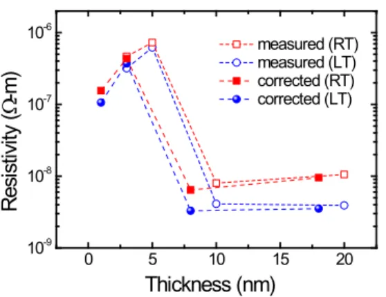
FIG. 5. Normal-state resistivity of the four samples at room and low temperatures. The measured resistivity (open symbols) calculated from the grown thickness and the corrected ones (solid symbols) that considered the native oxide layer. An anomalous drop of resistivity of sample A (3-nm Al) is clearly observed.
Figure5shows the normal-state resistivity of the four samples measured at room temperature (RT) and 4 K (LT). Standard four-terminal measurements were done with the sample size of 800 or 1600 µm in length and 100 µm in width. All the contacts of the large-size Hall bar are ohmic indicates that the Al films are continuous even down to the 3-nm one. The measured resistivity is calculated with the deposited thickness of Al and the corrected ones took the oxidation layer (2 nm for all the samples) into account. Three points need to be addressed in Figure5. (1) The very low resistivities (510-8Ω-m) of the 10-nm-thick and 20-nm-thick samples reveal the grown Al films are of high-quality. (2) The difference between the LT and RT resistivity decreases with the decreasing thickness because the size effect dominates over the phonon scattering in these films. (3) A clear drop of resistivity (either RT or LT) for the thinnest sample (sample A), that cannot be explained with the classical theory because the resistivity should have been increasing with the decreasing film thickness. One possible explanation is the existence of electronic quantum size effect in sample A.6,19,23,24 It could be the first room-temperature observation of quantum size effect in metals but further investigations are certainly needed to confirm this point. In addition, even for sample A of 3-nm Al, the room-temperature resistivity is as low as 10-7Ω-m, which enables the applications such as transparent electrodes in light emitting devices.
It is known that bulk Al is a superconductor with the critical temperature Tcof ∼1.2 K.7,22We measured the superconductivity in our samples but the lowest temperature for the used4He system is about 1.4 K. Figure6shows the resistance measurement as a function of applied magnetic field at various temperatures on sample B. At the lowest temperature of 1.37 K, we observe vanishing
FIG. 6. Superconducting state and critical temperatures of the four samples. Measured resistance as a function of applied magnetic field at various temperatures. The field was applied perpendicularly to the film plane. Inset: extracted superconducting critical temperature for the four samples showing a trend of increasing critical temperature with decreasing Al thickness.
075213-6 Fan et al. AIP Advances 7, 075213 (2017) resistivity near H = 0. For a given temperature, once the applied magnetic field reaches a certain value, the resistance shows a dramatic increase and reaches its normal-state saturation value of about 950 Ω. This can be ascribed to suppressed superconductivity in an applied H. By plotting the function
Hc(T ) from the resistance mid points at various temperatures, we can extract the critical temperatures
Tcof samples A and B. For sample C, the Tcwas obtained with the temperature-dependent resistivity measurement. The Tcfor sample D is lower than 1.4 K, out of the scope of our system. In the Inset of Figure6, we plotted Tcfor the four samples. Clearly, Tcincreases with decreasing Al thickness. The highest Tcobtained with sample A is about 2.5 K, which is more than two-times higher than its bulk value. Theoretical calculation of the quantum size effect on superconductivity predicts an increasing and oscillating Tcwith decreasing thickness in atomic scale.25Our atomic-scale Al films consist of various numbers of monolayers so the oscillating behavior could be washed out but the increase of
Tcis maintained.
IV. CONCLUSION
In conclusion, we have presented a study of high-quality atomic-scale aluminum films grown on 2-inch GaAs substrates by using a conventional MBE system. The smooth surface and nearly defect-free crystalline structure have been clearly evidenced by AFM, XRD, and TEM. The optical and electrical characterizations exhibit intriguing properties and give hints for quantized electronic states in the atomic-scale Al films. The self-protection oxide layer and large area fabrication of the grown Al film make it a promising candidate for further fundamental studies and future device applications using quantum size effect in metals.
ACKNOWLEDGMENTS
The authors acknowledge the technical support from the Center of Nano Science and Technology and the Center of Nano Facility at National Chiao Tung University, Integrated Service Technology Co. Ltd. and National Device Laboratory. This work was financially supported by the MOE ATU program and by MOST in Taiwan.
1T. W. Larsen, K. D. Pertersson, T. S. Jespersen, P. Krogstrup, J. Nygard, and C. M. Marcus, Phys. Rev. Lett. 115, 083110
(2015).
2P. Biagioni, J. S. Huang, L. Duo, M. Finazzi, and B. Hecht,Phys. Rev. Lett.102, 256801 (2009).
3H. W. Liu, F. C. Lin, S. W. Lin, J. Y. Wu, B. T. Chou, K. J. Lai, S. D. Lin, and J. S. Huang,ACS Nano9, 3875 (2015). 4Y. J. Lu, J. Kim, H. Y. Chen, C. Wu, N. Dabidian, C. E. Sanders, C. Y. Wang, M. Y. Lu, B. H. Li, X. Qiu, W. H. Chang,
L. J. Chen, G. Shvets, C. K. Shih, and S. Gwo,Science337, 450 (2012).
5B.-T. Chou, Y.-H. Chou, Y.-M. Wu, Y.-C. Chung, W.-J. Hsueh, S.-W. Lin, T.-C. Lu, T.-R. Lin, and S.-D. Lin,Sci. Rep.6,
19887 (2016).
6S. W. Lin, J. Y. Wu, S. D. Lin, M. C. Lo, M. H. Lin, C. T. Liang, and S. D. Lin,Jpn. J. Appl. Phys.52, 045801 (2013). 7C.-T. Liang, M.-R. Yeh, S. D. Lin, S. W. Lin, J. Y. Wu, T. L. Lin, and K.Y. Chen, Chinese J. Phys. 50, 638 (2012). 8D.-A. Luh, T. Miller, J. J. Paggel, M. Y. Chou, and T.-C. Chiang,Science292, 1131 (2001).
9M. M. Ozer, C.-Z. Wang, Z. Zhang, and H. H. Weitering,J. Low Temp. Phys.157, 221 (2009). 10W. Ming, S. Blair, and F. Liu,J. Phys.: Condens. Matter26, 505302 (2014).
11J. C. Boettger,Phys. Rev. B53, 13133 (1996).
12Y. Chen, A. A. Shanenko, P. Perali, and F. M. Peeters,J. Phys.: Condens. Matter24, 185701 (2012). 13A. Y. Cho and P. D. Derrier,J. Appl. Phys.49, 3328 (1978).
14S. Qin, J. Kim, Q. Niu, and C. K. Shih,Science324, 1314 (2009).
15P. S. Kirchmann, L. Rettig, X. Zubizarreta, V. M. Silkin, E. V. Chulkov, and U. Bovensiepen,Nat. Phys.6, 782 (2010). 16T. Zhang, P. Cheng, W. J. Li, Y. J. Sun, G. Wang, Z. G. Zhu, K. He, L. Wang, X. Ma, X. Cheng, Y. Wang, Y. Liu, H. Q. Lin,
J. F. Jia, and Q. K. Xue,Nat. Phys.6, 104 (2010).
17J. Kim, S. Qin, W. Yao, Q. Niu, M. Y. Chou, and C. K. Shih,Proc. Natl. Acad. Sci. USA107, 12761 (2010). 18Z. Yuan, Y. Jiang, Y. Gao, M. K¨all, and S. Gao,Phys. Rev. B83, 165452 (2011).
19M. Jalochowski and E. Bauer,Phys. Rev. B38, 5272 (1988).
20C. Brun, T. Cren, V. Cherkez, F. Debontridder, S. Pons, D. Fokin, M. C. Tringides, S. Bozhko, L. B. Ioffe, B. L. Altshuler,
and D. Roditchev,Nat. Phys.10, 444 (2014).
21H. M. Zhang, Y. Sun, W. Li, J. P. Peng, C. L. Song, Y. Xing, Q. Zhang, J. Guan, Z. Li, Y. Zhao, S. Ji, L. Wang, K. He,
X. Chen, L. Gu, L. Ling, M. Tian, L. Li, X. C. Xie, J. Liu, H. Yang, Q. K. Xue, J. Wang, and X. Ma,Phys. Rev. Lett.114, 107003 (2015).
22N. W. Ashcroft and N. D. Mermin, ‘Solid State Physics’, p. 233 (1976).
23S. W. Lin, Y. H. Wu, L. Chang, C. T. Liang, and S. D. Lin,Nanoscale Res. Lett.10, 71 (2015). 24S. T. Lo, S. W. Lin, Y. T. Wang, S. D. Lin, and C. T. Liang,Sci. Rep.4, 5438 (2014). 25P. Wojcik,ACTA Phys. Pol. A126, A-130 (2014).