Charge storage characteristics of Mo nanocrystal dependence on Mo oxide
reduction
Chao-Cheng Lin, Ting-Chang Chang, Chun-Hao Tu, Wei-Ren Chen, Chih-Wei Hu, Simon M. Sze, Tseung-Yuen Tseng, Sheng-Chi Chen, and Jian-Yang Lin
Citation: Applied Physics Letters 93, 222101 (2008); doi: 10.1063/1.3039065 View online: http://dx.doi.org/10.1063/1.3039065
View Table of Contents: http://scitation.aip.org/content/aip/journal/apl/93/22?ver=pdfcov
Published by the AIP Publishing
Articles you may be interested in
Physical and electrical characteristics of atomic layer deposited TiN nanocrystal memory capacitors
Appl. Phys. Lett. 91, 043114 (2007); 10.1063/1.2766680
Highly thermally stable TiN nanocrystals as charge trapping sites for nonvolatile memory device applications
Appl. Phys. Lett. 86, 123110 (2005); 10.1063/1.1890481
Effect of germanium concentration and tunnel oxide thickness on nanocrystal formation and charge storage/retention characteristics of a trilayer memory structure
Appl. Phys. Lett. 83, 3558 (2003); 10.1063/1.1615840
Observation of memory effect in germanium nanocrystals embedded in an amorphous silicon oxide matrix of a metal–insulator– semiconductor structure
Appl. Phys. Lett. 80, 2014 (2002); 10.1063/1.1459760
Enhancement on field-emission characteristics of diamondlike coated Mo substrates by redox process
J. Vac. Sci. Technol. B 19, 1739 (2001); 10.1116/1.1394726
This article is copyrighted as indicated in the article. Reuse of AIP content is subject to the terms at: http://scitation.aip.org/termsconditions. Downloaded to IP: 140.113.38.11 On: Wed, 30 Apr 2014 22:48:52
Charge storage characteristics of Mo nanocrystal dependence
on Mo oxide reduction
Chao-Cheng Lin,1Ting-Chang Chang,2,a兲 Chun-Hao Tu,1Wei-Ren Chen,1Chih-Wei Hu,1 Simon M. Sze,1Tseung-Yuen Tseng,1Sheng-Chi Chen,3and Jian-Yang Lin3
1
Institute of Electronics, National Chiao Tung University, Hsin-Chu 300, Taiwan
2
Department of Physics and Institute of Electro-Optical Engineering, Center for Nanoscience and Nanotechnology, National Sun Yat-Sen University, 70 Lien-hai Road, Kaohsiung 804, Taiwan
3
Department of Opto-Electronic Engineering, National Yunlin University of Science and Technology, Yunlin 64002, Taiwan
共Received 17 July 2008; accepted 9 November 2008; published online 1 December 2008兲 An oxygen incorporated Mo silicide was explored to form the Mo nanocrystals after rapid thermal annealing. Transmission electron microscopy showed the nanocrystals embedded in SiOx. Charge
storage characteristics of Mo nanocrystals influenced by the Mo oxide and the surrounding oxide were investigated through x-ray photoelectron spectroscopy and the electrical measurement. X-ray photoelectron spectra analyses revealed the redox reaction in the oxygen incorporated Mo silicide layer after rapid thermal annealing. The memory window and retention were improved due to reduction in Mo oxide. © 2008 American Institute of Physics. 关DOI:10.1063/1.3039065兴
In recent years, discrete nanocrystals composed floating gate nonvolatile memory structure has been widely investi-gated as a candidate for next generation nonvolatile memory because charges stored in lateral isolated nanocrystals in-stead of continuous conducting polycrystalline silicon layer are more immune to the local defect chain in the tunnel oxide.1–4 Many materials, such as Si, Ge, Ni, and Co, have been proposed to fabricate nanocrystal memory.2–6 Because of benefits on strong coupling, deep quantum well, and large density of state, metal nanocrystals have recently received much attention for research.5–7 However, the use of metal must take thermal stability issue into account because the metal diffusion into or chemical reaction with tunnel oxide during the memory fabrication process will compromise the performance of the memory structure.6 Mo is an attractive candidate because of its high work function, compatible with complementary metal-oxide-semiconductor process and high thermal stability.8
In this study, nonvolatile memory characteristics of Mo nanocrystals embedded in SiOxwere investigated by thermal
annealing oxygen incorporated Mo silicide layer. Our experi-ment results show that the Mo oxide was formed in the as-deposited layer. Lee et al.9 proposed that the formation of metal oxide during the nanocrystal fabrication process re-duces charge storage ability. To reduce the metal oxide, they need to perform a long-term thermal treatment in hydrogen ambience. In our investigation, we found that the Mo oxide was reduced after a critical annealing temperature, and this result improved the charge storage ability of Mo nanocrystal memory cell.
The memory cell structures were fabricated on a 6 in.
p-type Si substrate. A 5-nm-thick dry oxide 共tunnel oxide兲
was thermally grown at 950 ° C on the substrate in a hori-zontal furnace after the substrate was cleaned by Radio Corporation of America process. An 8-nm-thick oxygen in-corporated Mo silicide layer was deposited on the tunnel oxide by cosputtering Mo and Si targets in Ar共24 SCCM兲/O2
共2 SCCM兲 共SCCM denotes standard cubic centimeter per minute at STP兲 ambience. Subsequently, a 30-nm-thick sili-con dioxide 共blocking oxide兲 was deposited on the layer by plasma enhanced chemical vapor deposition at 300 ° C. Thermal annealing process at 800 and 900 ° C was per-formed in N2 for 60 s to investigate the temperature’s influ-ence on the memory characteristics of oxygen incorporated silicide layer. Finally, a 500-nm-thick Al gate patterned with shadow mask was evaporated by thermal coater to form the memory structures. Transmission electron microscopy 共TEM兲 and x-ray photoelectron spectroscopy 共XPS兲 were used to analyze the microstructure and chemical composition of nanocrystals and their surrounding oxide. Electrical char-acteristics of the capacitance-voltage 共C-V兲 hysteresis were measured by HP4284 Precision LCR Meter with frequency of 1 MHz.
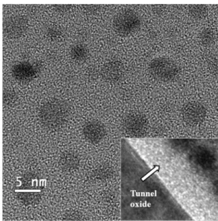
Figure 1 shows the plane-view TEM image of 900 ° C
a兲Electronic mail: [email protected]. FIG. 1. Plane-view and cross-sectionalcrystals embedded in SiO 共inset兲 TEM analyses of Mo nano-x.
APPLIED PHYSICS LETTERS 93, 222101共2008兲
0003-6951/2008/93共22兲/222101/3/$23.00 93, 222101-1 © 2008 American Institute of Physics
This article is copyrighted as indicated in the article. Reuse of AIP content is subject to the terms at: http://scitation.aip.org/termsconditions. Downloaded to IP: 140.113.38.11 On: Wed, 30 Apr 2014 22:48:52
sample to observe the microstructure of nanocrystals. The average diameter of the nanocrytals is approximately 4 nm and the area density of the nanocrytals is estimated to be about 1.01⫻1012 cm−2. The cross-sectional TEM image 共in-set of Fig. 1兲 shows a clear interface of tunnel oxide.
Be-sides, secondary ion mass spectra results 共unshown兲 exhibit that the position of Mo atom was unchanged between the tunnel oxide and the blocking oxide after 900 ° C annealing. This is important because metal atoms that diffuse into tun-nel oxide would deteriorate the reliability of the nonvolatile memory.
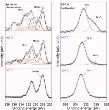
To investigate the chemical composition of oxygen in-corporated Mo silicide layer after annealing, the XPS analy-ses were performed by using an Al K␣ 共1486.6 eV兲 x-ray. Figures2共a兲and2共b兲 show the XPS Mo 3d and O 1s core-level spectra, respectively. The Mo 3d spectra of as-deposited sample show Mo–Mo and Mo–O bonds indicating the existence of metallic Mo and Mo oxides that correspond to various oxidation states 共Mo6+, Mo5+, Mo4+, and Mo3+兲.10–13
The 800 ° C annealed samples also contain me-tallic Mo and Mo oxides, but the area of Mo–O bonds is less than that for as-deposited sample in Fig. 2共a兲. After the 900 ° C annealing, there is only metallic Mo in the oxygen incorporated layer, as shown in Fig. 2共a兲. The XPS Mo 3d shows that the Mo oxides were reduced as the annealing temperature was increased. In Fig. 2共b兲, the O 1s spectra of as-deposited and 800 ° C annealed samples show Mo–O and Si–O bonds. The XPS peak of Si–O bond for as-deposited sample is less than 533.4 eV 共the binding energy of SiO2兲, which indicates that the oxide around Mo nanocrystals is deficient 共SiOx, x⬍2兲 in the oxygen incorporated layer.
There are only Si–O bonds, and the peak position of Si–O bonds shift toward higher binding energy for the sample after 900 ° C annealing. According to literature, the increment of O 1s binding energy is attributed to the oxygen bonding with
deficient silicon oxide.14The XPS results show that a redox between MoOxand SiOxoccurred during the thermal
anneal-ing process. For the redox behavior in the oxygen incorpo-rated Mo silicide layer, we consider that the formation en-ergy of Si oxide 共−750 kJ/mole兲 is larger than that of Mo oxide 共−450 kJ/mole兲.15 Therefore, the oxygen of Mo ox-ides prefers to bond with Si than Mo during the thermal annealing at 900 ° C, which results in the reduction in Mo oxide and improved the quality of SiOx.
Figure3shows the comparison of the C-V curves for the 800 and 900 ° C annealed samples. The curves were obtained after the gate voltage swept from inversion to accumulation region of the substrate 共from 9 to −11 V兲 and the reverse 共from −11 to 9 V兲. The hysteresis loop of the samples is counterclockwise due to substrate injection through the tun-nel oxide. We note that the memory window 共the width of the loop兲 for 900 °C annealed sample is twice larger than that for 800 ° C one. According to XPS results, we speculate that the larger memory window for 900 ° C annealed sample was due to the reduction in Mo oxide that was proposed as a semiconductorlike metal oxide. Therefore, the Mo oxide has lower density of state than metallic Mo for the charge stor-age.
Figure 4 shows the retention behavior of 800 and 900 ° C samples. The retention was measured by stress volt-age of 10 V on gate electrode for 5 s. The memory window is obtained by comparing the C-V curves of a charged state
FIG. 2. 共Color online兲 共a兲 Mo 3d and 共b兲 O 1s core-level spectra of the oxygen incorporated Mo silicide layer for as-deposited, 800, and 900 ° C annealed samples. The Mo–O bonds in Mo 3d spectra originated from vari-ous oxidation states, Mo3+共triangle兲, Mo4+共gray circle兲, Mo5+共square兲, and
Mo6+共diamond兲.
FIG. 3. 共Color online兲 The comparison of the C-V curves of the samples annealed at 800 and 900 ° C.
FIG. 4. 共Color online兲 the retention behavior of samples annealed at 800 °C 共remained charges of 11%兲 and 900 °C 共remained charges of 74%兲.
222101-2 Lin et al. Appl. Phys. Lett. 93, 222101共2008兲
This article is copyrighted as indicated in the article. Reuse of AIP content is subject to the terms at: http://scitation.aip.org/termsconditions. Downloaded to IP: 140.113.38.11 On: Wed, 30 Apr 2014 22:48:52
to a quasineutral state. It can be found that the memory win-dow of 800 ° C annealed sample decreased significantly and remained ⬃11% after 104 s. In contrast, the retention of 900 ° C annealed sample remained ⬃74%. From the XPS results 共Fig.2兲, the different retention behavior was
consid-ered to be due to the quality of the surrounding oxide. When charges are stored in the nanocrystals, the stored charges can escape laterally through the traps in the surrounding oxide. If the tunnel oxide has a leakage path, the lateral escaped charges will leak into the substrate. Because the surrounding oxide quality of 900 ° C annealed sample was improved by the redox reaction between Mo oxide and SiOx, more charges
can remain in the Mo nanocrystals.
In conclusion, Mo nanocrystals were fabricated for non-volatile memory application through thermal annealing of oxygen incorporated Mo silicide layer. The average size and density of Mo nanocrystals were estimated to be about 4 nm and 1⫻10−12, respectively. The XPS results indicate the ex-istence of Mo oxide and SiOx in oxygen incorporated Mo
silicide layer after 800 ° C annealing, and the Mo oxide was reduced after 900 ° C annealing. The 900 ° C annealed sample has the better retention共74%兲 and the larger memory window共3.6 V兲 than the 800 °C one due to the reduction in Mo oxide.
This work was performed at National Nano Device Laboratories, Taiwan, R.O.C. The authors would like to
ac-knowledge the financial support of the National Science Council 共NSC兲 under Contract Nos. NSC 96-2221-E-009-202-MY3, NSC 96-2112-M-110-013, and NSC-97-3114-M-110-001.
1S. Tiwari, F. Rana, K. Chan, H. Hanafi, W. Chan, and D. Buchanan, Tech
Dig. Int. Electron Devices Meet. 1995, 521.
2S. Tiwari, F. Rana, H. Hanafi, A. Hartstein, E. F. Crabbe, and K. Chan, Appl. Phys. Lett. 68, 1377共1996兲.
3J. D. Blauwe, IEEE Trans. Nanotechnol. 1, 72共2002兲.
4C. H. Tu, T. C. Chang, P. T. Liu, H. C. Liu, S. M. Sze, and C. Y. Chang,
Appl. Phys. Lett. 89, 16215共2006兲.
5S. Tang, C. Mao, Y. Liu, D. Q. Kelly, and S. K. Banerjee, IEEE Electron
Device Lett. 54, 433共2007兲.
6J. Dufourcq, P. Murb, M. J. Gordonc, S. Minoretb, R. Copparda, and T.
Baron,Mater. Sci. Eng., C 27, 1496共2007兲.
7Z. Liu, C. Lee, V. Narayanan, G. Pei, and E. C. Kan, IEEE Electron
Device Lett. 49, 1606共2002兲.
8T.-L. Li, W. L. Ho, H. B. Chen, H. C. H. Wang, C. Y. Chang, and C. Hu, IEEE Trans. Electron Devices 53, 1420共2006兲.
9C. Lee, J. H. Kwon, J. S. Lee, Y. M. Kim, Y. Choi, H. Shin, J. Lee, and B.
H. Sohn,Appl. Phys. Lett. 91, 153506共2007兲.
10C. B. Roxlo, H. W. Deckman, J. Gland, S. D. Cameron, and R. R.
Chianelli, Science 235, 1629共1987兲.
11Y. C. Lu and C. R. Clayton,Corros. Sci. 29, 927共1989兲.
12T. S. Sian and G. B. Reddy,Sol. Energy Mater. Sol. Cells 82, 375共2004兲. 13J. F. Moulder, W. F. Stickle, P. E. Sobol, and K. D. Bomben, Handbook of
X-ray Photoelectron Spectroscopy共Perkin-Elmer, Minnesota, 1992兲.
14J. X. Wu, M. S. Ma, H. G. Zheng, H. W. Yang, J. S. Zhu, and M. R. Ji, Phys. Rev. B 60, 17102共1999兲.
15R. Mitra, Int. Mater. Rev. 51, 13共2006兲.
222101-3 Lin et al. Appl. Phys. Lett. 93, 222101共2008兲
This article is copyrighted as indicated in the article. Reuse of AIP content is subject to the terms at: http://scitation.aip.org/termsconditions. Downloaded to IP: 140.113.38.11 On: Wed, 30 Apr 2014 22:48:52