High-energy ion implantation of silicon has been extensively uti-lized in the deep submicrometer ultralarge-scale integration (ULSI) regime.1-3It can be used to fabricate many novel structures, such as triple well, retrograde well, and retrograde well with buried layer.1,2,4-6 These structures can be fabricated to optimize many device characteristics almost independently, such as channel mobil-ity, punch-through voltage, junction capacitance, latchup suscepti-bility, soft-error immunity, etc., by employing multiple high-energy ion implantation.1-3
However, there is a concern about the high-energy ion implanta-tion regarding the secondary defects in the substrates that are formed during the postimplantation thermal annealing process. The incom-ing ions produce a large number of Frenkel pairs in the ion-implant-ed silicon, constituting the primary defect, and the secondary defect evolved from the primary defect during the postimplantation anneal-ing process.7Many studies have been devoted to this problem.8-12A number of techniques, including cross-sectional transmission elec-tron microscopy (XTEM), Rutherford backscattering/channeling spectroscopy (RBS), deep-level transient spectroscopy (DLTS), X-ray diffraction analysis (XRD), and electron paramagnetic reso-nance (EPR), have been used to investigate the nature and distribu-tion of these secondary defects.13-20Among the various techniques, XTEM is the most utilized one. However, the fabrication procedure of TEMs sample is complicated and time consuming. Moreover, XTEM cannot detect the defects at density below 107cm22, so that the presence of a low density of defects will probably be overlooked in XTEM observation, yet such a low density of defects in the device junction region may be detrimental to the device performance.11 Therefore, some other appropriate means are necessary to detect the presence of the defects induced by high-energy ion implantation.
In this work, we attempt to use a simple and effective method to delineate the residual defects in the megaelectronvolt high-energy ion implanted substrate after the postimplantation thermal annealing process. A preferential chemical etching solution consisted of CrO3, and HF acid was used for the defects delineation. This mixed solution of CrO3/HF has been used to delineate the dislocation-related defects formed during the crystal-growth of silicon.21-24 The delineated defects were then observed by scanning electron microscopy (SEM).
Experimental
The substrate used for the experiment of this work was (100) ori-ented, n-type silicon wafers of 8 in. diam with 2-5 V cm nominal resistivity. After the initial standard cleaning, the wafers were im-planted with boron ions at energies of 0.5, 1, and 2 MeV, separately,
to a dose of 3 3 1014cm22. The ion-implanted wafers were rapid thermal annealed (RTA) at 10008C for 30 s in N2ambient. After the
Detection of the Defects Induced by Boron High-Energy Ion
Implantation of Silicon
Wei-Cheng Hsu,
a,zMao-Chieh Chen,
a,*
,zand Mong-Song Liang
b aDepartment of Electronics Engineering, National Chiao Tung University, Hsinchu, TaiwanbTaiwan Semiconductor Manufacturing Company, Advanced Module Technology Division, Research and Development
Department, Hsinchu, Taiwan
A preferential chemical etching method was used to investigate the secondary defects induced in silicon by high-energy boron ion implantation followed by a rapid thermal anneal at 10008C for 30 s in N2ambient. The dislocation defects in silicon can be clear-ly delineated by the etchant of CrO3/HF mixing solution. Moreover, a band of striation corresponding to the region of dislocation defects can be observed from the cross-sectional view micrographs of scanning electron microscopy. For the high-energy boron ion implantation at a dose of 3 3 1014cm22and energies of 0.5 to 2 MeV studied in this work, the defect density is estimated to be in the order of 6 3 106cm22. Furthermore, we found a close correlation between the depth profiles of the observed etching pits
and that of the implantation-induced damage.
© 2000 The Electrochemical Society. S0013-4651(00)01-011-9. All rights reserved. Manuscript submitted January 4, 2000; revised manuscript received April 19, 2000.
* Electrochemical Society Active Member.
z E-mail: [email protected]
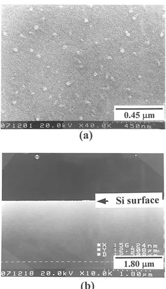
Figure 1. SEM micrographs of a control sample etched with a preferential etchant for 10 s. (a) Top-view and (b) cross-sectional view.
annealing process, all wafers were cut into pieces of 1 3 1 cm square for defects delineation with preferential chemical etching. Before the etching, the samples were dipped in flowing deionized (DI) water for 5 min to remove particles which may adhere to the surfaces of the samples that could disturb the etching results. The samples were etched in a preferential etching solution, which consists of one part by volume of 0.15 M CrO3in DI water and two parts by volume of HF (49%). The etching time ranged from 10 s to several minutes.
During the etching process, the samples were properly agitated in the etching solution to prevent gas bubbles from gathering on the sample surfaces, which could disturb the etching results. After the etching, the samples were dipped in flowing deionized water for 5 min. For comparison, wafers without high-energy ion implantation were also processed in the same etching scheme; samples derived from these wafers are designated as control samples hereafter. Scan-ning electron microscopy (SEM) was used to observe the surface
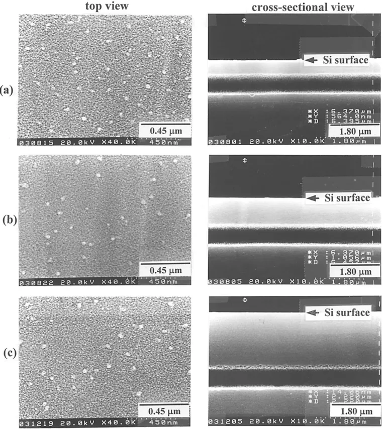
Figure 2. SEM micrographs showing top view (left) and cross-sectional view (right) of boron ion implanted samples etched in preferential etchant for 10 s; the boron ions are implanted to a dose of 3 3 1014cm22at an energy of (a) 0.5, (b) 1, and (c) 2 MeV.
morphology as well as the cross-sectional microstructure, and sec-ondary ion mass spectroscopy (SIMS) was used for elemental depth profile measurement. The transport of ions in matter (TRIM) was used to simulate the distribution of defects.
Results
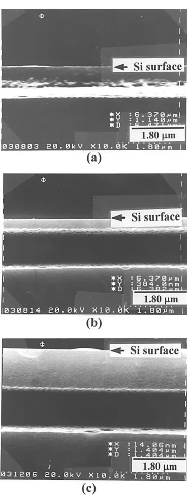
Figure 1 shows the top view and cross-sectional view SEM micrographs for the control sample etched in preferential etchant for 10 s. The substrate surface is very smooth, except that there are vis-ible white mounds on the top view, which are the artifacts formed in the CrO3/HF etching solution.21Figure 2 shows the top view and cross-sectional view SEM micrographs for the high-energy ion implanted samples that were preferentially etched for 10 s. It is found that all samples show a very smooth surface except for the appearance of the white mound artifacts. However, there are obvious bands of striation in the cross-sectional view; the distances from the top of striations to the etched substrate surfaces were measured to be 0.64, 1.00, and 2.16 mm, respectively, for the samples implanted at energies of 0.5, 1, and 2 MeV. Figure 3 shows the cross-sectional view SEM micrographs for the high-energy ion implanted samples that were preferentially etched for 50 s; it is found that the width of the striations increased with the etching time. Prolonged etching removed a thicker layer from the Si wafer and the etching rate was determined to be about 0.6 mm/min. The SEM micrographs in Fig. 4 show the surface morphologies of 0.5 MeV implanted samples after preferential chemical etching for 50 and 140 s, which correspond to a removal of a 0.5 and 1.4 mm thick surface layers, respectively, from the Si wafer. A large number of etching pits appear on the sur-faces of the etched samples. For the sample etched to remove a 0.5mm thick surface layer, the etching pit has a density of 2.6 3 105cm22and the size of the etching pits is about 0.72 mm (Fig. 4a). As the sample was etched to remove 1.4 mm thick surface layer, the density of etching pits increases to 6.0 3 106cm22while the size is measured to be about 0.63 mm (Fig. 4b).
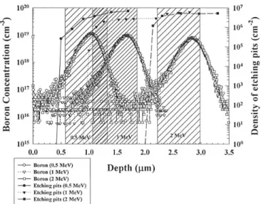
Figure 5 and 6 show, respectively, surface morphologies of the 1 and 2 MeV implanted samples that were etched in preferential etchant for various times. Etching pits, similar to those found on the 0.5 MeV implanted samples, appeared on the etched surface. For the 1 MeV implanted sample, removal of a 1 mm thick surface layer by the preferential etchant revealed etching pits with a density of 7.4 3 104cm22and a pit size of about 1.2 mm (Fig. 5a). We found an increasing density of the etch pits as the etching time was increased. After a preferential etch of 4 min, which corresponds to a removal of 2.4 mm thick surface layer, the density of etch pits was increased to 4.9 3 106cm22(Fig. 5b). Similar observation was obtained on the 2 MeV implanted samples (Fig. 6). The 4.4 min etched sample, which corresponds to a removal of 2.6 mm thick surface layer, revealed etch pits with a density of 5.3 3 106cm22. The density of etch pits increases with increasing etching time. The etch pits distri-bution as well as the boron concentration profiles of the boron ion implanted sampled are illustrated in Fig. 7.
Discussion
Chemical etching of the silicon surface is determined by two basic reactions: oxidation of silicon and the following dissolution of the oxide. Consequently, typical etchants contain a strong oxidizing agent in association with hydrofluoric acid that dissolves the oxides of sili-con. Chemical etching for defect delineation depends upon the prop-erty that the oxidation rate of the silicon at the site of the defect is sig-nificantly different from that at defect-free regions of the crystal. The oxidation rate at the defect is greater than that of the surrounding region, giving rise to etch pits that can be clearly observed.25
The formation of a dislocation pit arises mainly from the strain field associated with a dislocation and/or impurities segregated at a dislocation. The strain field and/or the impurity segregation produce a surface potential difference between the site of a dislocation and the surrounding perfect crystal, which in turn causes a difference in the etching rate. During the process of etching, HF dissolves silicon oxide when the silicon surface is oxidized by CrO3. In the present Figure 3. SEM micrographs showing a cross-sectional view of boron ion
implanted samples etched in preferential etchant for 50 s; the boron ions are implanted to a dose of 3 3 1014cm22at an energy of (a) 0.5, (b) 1, and (c)
Figure 4. SEM micrographs showing the surfaces of silicon wafers implanted with boron ions at 0.5 MeV to a dose of 3 3 1014cm22followed by preferential
etching to remove a surface layer of (a) 0.5 and (b) 1.4 mm.
Figure 5. SEM micrographs showing the surfaces of silicon wafers implanted with boron ions at 1 MeV to a dose of 3 3 1014cm22followed by preferential
work, etch pits of dislocation were found to be oriented in the [110] direction, similar to those reported in literature.7,8,10
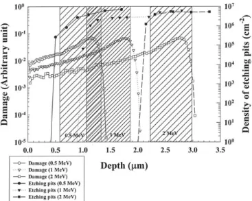
Figure 7 shows the boron concentration profiles and the etch pits distribution in the boron ion implanted samples; also shown are hatched areas, which represent the ranges of striation bands found in Fig. 2 from the cross-sectional view SEM micrographs. This indi-cates that the bands of striation in the cross-sectional view SEM micrographs correspond to the regions of dislocation defects, which were delineated as the etch pits by the preferential etchant. It is found that the bands of striation appeared as the etch pits reached a density of about 106cm22. The calculated damage profiles using the TRIM simulation are illustrated in Fig. 8 along with the observed etch pits distributions and the ranges of striation bands (i.e., the hatched areas), as shown in Fig. 7. We found that the depth profiles of the observed etch pits and that of the implantation-induced dam-age are closely correlated.
Conclusion
This work investigates the secondary defects induced by high-energy boron ion implantation using a preferential chemical etching method. The dislocation defects can be clearly delineated by the etchant of CrO3/HF mixing solution. Moreover, a band of striations corresponding to the region of dislocation defect density in excess of about 106cm22can be observed from the cross-sectional view SEM micrographs. For the high-energy boron ion implantation to a dose of 3 3 1014cm22at energies of 0.5 to 2 MeV studied in this work, the defect density is estimated to be in the order of 6 3 106cm22.
Fur-thermore, we found a close correlation between the depth profiles of the observed etch pits and that of the implntation-induced damage. Figure 6. SEM micrographs showing the surfaces of silicon wafers implanted with boron ions at 2 MeV to a dose of 3 3 1014cm22followed by preferential
etching to remove a surface layer of (a) 2.6 and (b) 3.3 mm.
Figure 7. Boron profiles and etch pits distribution for boron ion implanted samples; the Si samples were implanted with boron ions at an energy of 0.5, 1, and 2 MeV to a dose of 3 3 1014cm22followed by RTA anneal at 10008C
National Chiao Tung University assisted in meeting the publication costs of this article.
References
1. K. Tsukamoto, S. Komori, T. Kuroi, and Y. Akasaka, Nucl. Instrum. Methods Phys.
Res. Sect. B, 59/60, 584 (1991).
2. K. Tsukamoto, T. Kuroi, S. Komori, and Y. Akasaka, Solid State Technol., 35, 49 (1992).
3. J. O. Borland and R. Koelsch, Solid State Technol., 36, 28 (1993).
4. S. Fujii, M. Oogihara, M. Shimizu, M. Yoshida, K. Numata, T. Hara, S. Watanabe, S. Sawada, T. Mizuno, J. Kumagai, S. Yoshikawa, S. Kaki, Y. Saito, H. Aochi, T. Hamamoto, and K. Toita, IEEE J. Solid-State Circ., 24, 1170 (1989).
5. A. Umezawa, S. Atsumi, M. Kuriyama, H. Banba, K. Imamiya, K. Naruke, S. Yamada, E. Obi, M. Oshikiri, T. Suzuki, and S. Tanaka, IEEE J. Solid State Circ., 27, 1540 (1992).
6. T. Jinbo, H. Nakata, K. Hashimoto, T. Watanabe, K. Ninomiya, T. Urai, M. Koike, T. Sato, N. Kodama, K. Oyama, and T. Okazawa, IEEE J. Solid State Circ., 27, 1547 (1992).
7. K. Seshan and J. Washburn, Radiat. Eff., 37, 147 (1978).
8. M. Tamura, N. Natsuaki, Y. Wada, and E. Mitani, J. Appl. Phys., 59, 3417 (1986). 9. M. Tamura, N. Natsuaki, Y. Wada, and E. Mitani, Nucl. Instrum. Methods Phys.
Res. Sect. B, 21, 438 (1987).
10. N. W. Cheung, C. L. Liang, B. K. Liew, R. H. Mutikainen, and H. Wong, Nucl.
Instrum. Methods Phys. Res. Sect. B, 37/38, 941 (1989).
11. M. Tamura and N. Natsuaki, Nucl. Instrum. Methods Phys. Res. Sect. B, 39, 318 (1989).
12. J. Y. Chang, D. J. Eaglesham, D. C. Jacobson, P. A. Stolk, J. L. Benton, and J. M. Poate, J. Appl. Phys., 80, 2105 (1996).
13. O. W. Holland, M. K. El-Ghor, and C. W. White, Appl. Phys. Lett., 53, 1282 (1996). 14. A. Hallén and B. G. Svensson, Nucl. Instrum. Methods Phys. Res. Sect. B, 80/81,
106 (1993).
15. R. Fabbri, G. Lulli, R. Nipoti, and M. Sevidori, Nucl. Instrum. Methods Phys. Res.
Sect. B, 80/81, 624 (1993).
16. T. A. Belykh, A. L. Gorodishchensky, L. A. Kazak, V. E. Semyannikov, and A. R. Urmanov, Nucl. Instrum. Methods Phys. Res. Sect. B, 51, 242 (1990).
17. T. P. Sjoreen, O. W. Holland, M. K. El-Ghor, and C. W. White, Mater. Res. Soc.
Symp. Proc., 128, 593(1989).
18. H. Sayama, A. Kinomura, Y. Yuba, and M. Takai, Nucl. Instrum. Methods Phys.
Res. Sect. B, 80/81, 587 (1993).
19. J. G. E. Klappe, I. Bársony, J. R. Liefting, and T. W. Ryan, Thin Solid Films, 235, 189 (1990).
20. L. Sealy, R. C. Barklie, W. L. Brown, and D. C. Jaconson, Nucl. Instrum. Methods
Phys. Res. Sect. B, 80/81, 528 (1993).
21. F. S. d’ Aragona, J. Electrochem. Soc., 119, 948 (1972). 22. M. W. Jenkins, J. Electrochem. Soc., 124, 757 (1977). 23. D. G. Schimmel, J. Electrochem. Soc., 126, 479 (1979). 24. K. H. Yang, J. Electrochem. Soc., 131, 1140 (1984).
25. K. V. Ravi, Imperfections and Imurities in Semiconductor Silicon, p. 197, John Wiley & Sons, Inc., New York (1991).
Figure 8. Damage profiles and etch pits distribution for boron ion implanted samples; the Si samples were implanted with boron ions at an energy of 0.5, 1, and 2 MeV to a dose of 3 3 1014cm22followed by an RTA anneal at