行政院國家科學委員會專題研究計畫 成果報告
掃描鏈中多重時間錯誤之診斷
計畫類別: 個別型計畫 計畫編號: NSC93-2215-E-002-030- 執行期間: 93 年 08 月 01 日至 94 年 10 月 31 日 執行單位: 國立臺灣大學電子工程學研究所 計畫主持人: 李建模 報告類型: 精簡報告 處理方式: 本計畫可公開查詢中 華 民 國 94 年 10 月 28 日
行政院國家科學委員會補助專題研究計畫成果報告
※※※※※※※※※※※※※※※※※※※※※※※※※※
※
掃描鏈中多重時間錯誤之診斷
※
※※※※※※※※※※※※※※※※※※※※※※※※※※
計畫類別:■個別型計畫(小產學) □整合型計畫
計畫編號:NSC93-2215-E-002-030
執行期間: 93 年 8 月 1 日 至 94 年 10 月 31 日
計畫主持人:李建模 博士
計畫參與人員: 莊惟舜
執行單位:台灣大學電子工程研究所
中 華 民 國 94 年 10 月 27
中、英文摘要
本研究計畫展示一個定位掃描鍊上維持與設定時間錯誤的診斷技術。這個 技術利用溫測掃描輸入樣式,只有一個上升或下降的轉換,達成了決定性 的診斷結果。有了溫測掃描輸入樣式,診斷樣式也可經由些微修改現有的 單一固接錯誤測試樣式來產生。
This report presents a diagnosis technique to locate hold-time (HT) faults and setup-time (ST) faults in scan chains. This technique achieves deterministic diagnosis results by applying thermometer scan input (TSI) patterns, which have only one rising or one falling transition. With TSI patterns, the diagnosis patterns can be easily generated by existing single stuck-at fault test pattern generators with few modifications.
關鍵詞:
錯誤診斷,自動測試樣式產生機,掃描鍊
報告內容:
I. INTRODUCTION
This paper presents a technique to diagnose multiple hold-time (HT) faults and setup-time (ST) faults in scan chains. The HT and ST fault models have been proposed by previous research [1] and real diagnostic cases have recently been reported [2][3][4]. HT faults occur when the delay from one scan cell to its neighbor is shorter than the required hold time. The mux-scan flip-flop style designs are especially susceptible to HT faults. Changing the style of scan design may avoid HT faults but diagnosing these faults is still essential for chips that are already designed and manufactured. ST faults occur when the delay from one scan cell to its neighbor is longer than expected. ST faults can be caused by signal integrity problems or by routing congestion. Although ST faults can be eliminated by lowering the speed of scan chain shifting [5], diagnosis of ST faults is important to identify the root cause and save the test application time.
Past research in scan chain diagnosis can be classified into hardware solutions and software solutions. In the hardware category, Schafer proposes to add extra routings from one scan chain to its partner scan chain [6]. Edirisooriya proposes to insert XOR gates into the scan chains so that the contents of the scan cells can be flipped before shifting into the next scan cell [7]. Wu and Narayanan propose to flip the contents of each scan cell by modifying the scan cell design [1], [8]. The hardware solutions require extra hardware and, what is worse, they are too late for chips that are already fabricated.
pattern generator (ATPG) to generate diagnosis patterns [9]. Hirase presents an IDDQ diagnosis technique in which one IDDQ is measured every time the scan chain is shifted by one bit [10]. Kundu’s and Hirase’s ideas are good for single stuck-at faults only, not for multiple faults. Stanley presents a score based diagnosis tool that does fault simulations for all latches in scan chains [11]. The score of a fault represents the degree of similarity between a circuit’s expected faulty outputs and its actual outputs. Guo proposes a three-step diagnosis procedure [3], [12]. Huang proposes a probabilistic model for intermittent timing faults in scan chains [2]. Their technique handles multiple faults by ranking the probability of a group of candidate faults. None of the above techniques produces deterministic diagnosis results in the presence of multiple faults in scan chains. IBM files a patent to diagnose ST faults by changing the speed of scan chain shifting [5]. This patent performs a slow speed shifting in suspicious intervals to locate the faulty scan cell(s) by binary search. This technique, although very useful for ST faults in LSSD designs, cannot diagnose HT faults in flip-flop designs.
The proposed diagnosis technique is divided into two parts. In the first part, the fault type, faulty chain, and the number of faults are determined. In the second part, the locations of the faults in the chains are diagnosed. The first advantage of the proposed technique is that it provides fine and deterministic diagnosis resolutions, even in the presence of multiple faults in a scan chain. This is achieved by applying
thermometer scan input (TSI) patterns, which have only one rising transition or one
falling transition. With TSI patterns, the diagnosis patterns can be generated by widely available SSF ATPG tools. This eliminates the need for a customized diagnosis pattern generator. The second important feature is that this technique diagnoses not only the first fault but also the remaining faults in a scan chain. This is accomplished by applying thermometer scan input with padding (TSIP) patterns, which are similar to TSI patterns except that the former have a specified number of pad bits. The last feature is that this technique generates dedicated diagnosis patterns, which are much shorter than regular ATPG patterns. This is especially useful when traditional diagnosis using regular ATPG patterns fails to produce fine diagnosis resolutions due to limited tester memory.
The organization of the paper is as follows. The second section introduces some basic terms and background knowledge. The third section shows how to determine the fault type and the number of faults. The fourth and fifth sections present the diagnosis techniques for the first and the remaining faults, respectively. The sixth section discusses some issues related to the technique and the last section summarizes this paper.
II. Background
A. Scan Chain Fault Models
The scan cells are indexed in descending order, from scan input (index = L-1) to scan output (index = 0). The length of the scan chain (L) is the total number of scan cells in the chain. For a given scan cell i, cells that are indexed higher or lower than
i are upstream or downstream to cell i, respectively [12]. Let j denote the scan clock
cycle number and let g(i,j) represent the good content of scan cell i at clock cycle j. Assuming no inversion between scan cells, the shift operation of a good chain is modeled by g(i+1, j) = g(i, j+1). Let a(i,j) denote the actual content of scan cell i at cycle j. For a faulty chain, the actual content of a faulty cell is different from its good content when certain excitation conditions are met. An ST fault in cell i is excited when cell i is expected to make a rising or falling transition in the current cycle — that is, g(i,j-1) ≠ g(i,j). The effect of ST fault is that cell i remains the previous value in the current cycle — that is, a(i,j)=g(i,j-1). An HT fault in cell i is excited when cell i is expected to make a rising or falling transition in the next clock cycle — that is, g(i,j+1) ≠ g(i,j). The effect of HT fault is that cell i makes the transition in the current cycle — that is, a(i,j)=g(i,j+1). The HT faulty cell can be regarded as a transparent buffer that bypasses the scan data without holding them [1], [12].
Causes of HT faults and ST faults can be classified into three major categories: the scan cell internal problems, the scan signal timing problems, and the clock timing problems. In the first category, defective transistors (such as leakage and incorrect implants) and highly resistive bridging defects are shown to be culprits for ST faults [13] and HT faults [4], respectively. For the second category, signal integrity problems such as crosstalk and ground bounce are responsible for scan chain faults in nano-meter technologies [2]. On top of that, ST faults can be caused by setup time violation due to routing congestion, especially when the router gives priority to functional signals over the scan signals. HT faults can be caused by hold-time violations due to insufficient buffers between scan flip-flops. The third category, clock skew, is the result of design errors or process defects. The mux-scan flip-flop style designs are especially susceptible to HT faults. HT faults occur if the active clock edge arrives the faulty cell i much later than its upstream cell i+1 [1]. Some of the scan chain faults are permanent (such as bridging, clock skew) and the others are intermittent (such as crosstalk). Please see the discussion section for more details about the intermittent fault diagnosis.
B. Thermometer Scan Input Patterns
Thermometer scan input (TSI) patterns are scan input patterns that have only one rising transition or one falling transition. Table I lists TSI patterns of length 2L,
which are evenly divided into two parts: the head portion and the tail portion. (Note that the rightmost bit is shifted into the chain first.) The underlined bits, which are flipped after the fault excitation, are called sensitive bits. By definition, there is only one sensitive bit in a TSI pattern. There are four types of TSI patterns: S10, H10, S01, and H01. The ‘01’ types have a group of ones followed by a group of zeros; the ‘10’ types have a group of zeros followed by a group of ones. TSI patterns for the ST fault, subscripted ‘S’, have sensitive bits equal to the tail portion. TSI patterns for the HT fault, subscripted ‘H’, have sensitive bits equal to the head portion. The reason why the sensitive bits are always placed at the end of the head portion will be clear in the coming sections.
TABLE I TSIPATTERNS OF LENGTH 2L Type Tail (length L) Head (length L) TS10 11111…1 10000…0 TH10 11111…1 00000…0 TS01 00000…0 01111…1 TH01 00000…0 11111…1
As a TSI pattern is shifting in a scan chain with a single fault, the sensitive bit is flipped as soon as it passes the faulty cell. To diagnose the single fault is to find out, as early as possible, where the sensitive bit is flipped. Things become more complicated in the presence of multiple faults. Figure 1 shows how the actual contents of scan cells change as the TH10 pattern shifts in a scan chain with two HT faults. Suppose that the first and the second faults are located in cell 11 and cell 8, respectively. (The nth fault, fn, is the faulty cell that has the nth highest index.)
When the sensitive bit reaches cell 11 in cycle j+1, it is flipped as if cell 11 is transparent. Similarly, in cycle j+3, faulty cell 8 is also flipped. The actual contents now have two flipped bits: the sensitive bit and its immediate downstream bit. It can be generalized that a TSI pattern has at most n flipped bits in the presence of n faults in a scan chain.
f1 12 11 10 9 8 7 6 5 4 3 2 1 0 f2 0 0 0 0 0 0 0 0 0 0 0 0 0 1 0/1 0 0 0 0 0 0 0 0 0 0 1 1 0/1 0 0 0 0 0 0 0 0 0 1 1 1 0/1 0 0 0 0 0 0 0 1 1 1 1 0/1 0/1 0 0 0 0 0 0 SI a(i,j+1) a(i,j+2) a(i, i+3) a(i,j) a(i,j+4) 0 0 0/1 0 0 Index
Figure 1. Contents of Scan Cells as TH10 shifts (double faults)
III. Determining Fault Types and Number of Faults
which cannot determine the number of faults in the presence of multiple faults. This paper proposes a two-pattern test (Table II) to determine the fault type as well as the number of faults in a scan chain. Each pattern is of equal length L. In the first pattern, the downstream half is all zeros and the upstream half is all ones. The second pattern is the bitwise complement of the first pattern. On the tester, the scan chain is initialized by shifting the first (the rightmost) bit of the first pattern for L times. Alternatively, the scan chain can be initialized by asserting the independent reset or preset signals if available. The first pattern is then scanned in, followed by an immediate scan out without any system clock. The scan outputs are recorded by the tester without an immediate pass/fail decision. The same procedure is repeated for the second pattern. If there exist f ST faults, there will be f more zeros and f more ones than expected in the first and the second scan outputs, respectively. Similarly, the number of HT faults can be counted in the similar way.
TABLE II
TWO TEST PATTERNS TO DETERMINE FAULT TYPE AND NUMBER OF FAULTS (2 FAULTS ASSUMED) Pattern Pattern 1 (L) Pattern 2 (L) Scan in (= expected scan
out)
11110000 00001111
Scan out of ST 11000000 00111111
Scan out of HT 11111100 00000011
The scan chains that fail either test are faulty; those chains that pass both tests are good. In the following section, the faulty chains are diagnosed one chain by one chain ⎯ that is, one scan chain under diagnosis (ChUD) at a time. The scan chains other than the ChUD are the scan chains under no diagnosis (ChUNDs). The ChUD must be faulty and ChUNDs can be either good or faulty.
IV. Diagnosis of the First Fault
Figure 2 illustrates the flow chart to diagnose the first fault in a circuit under
diagnosis (CUD). The combinational automatic diagnosis pattern generator
(C-ADPG) generates diagnosis patterns of coarse resolution within a short time whereas the sequential automatic diagnosis pattern generator (S-ADPG) generates diagnosis patterns of fine diagnosis resolutions at a cost of relatively long CPU time. The ADPG patterns include scan inputs (SI), primary inputs (PI), good primary outputs (POg), and good scan outputs (SOg). All the actually observed primary outputs (POa) and scan outputs (SOa) are logged into a file without an immediate pass/fail decision. Finally, POa and SOa are matched with POg and SOg off line to obtain the diagnosis results, the upper bound U(f1) and the lower bound L(f1) of the
C-ADPG, S-ADPG Match SI, PI ATE CUD U(f1), L(f1) POg, SOg POa,SOa
faulty chain, type, # of faults
Figure 2. Diagnosis the first fault A. C-ADPG
1.) Combinational Diagnosis Procedure, CDP
The CDP is applied to one single scan cell, the scan cell under diagnosis (CeUD), every time a ChUD is loaded. The CDP steps are as follows. (1) Initialize the ChUD by shifting in the first bit of the TSI pattern for L times. (2) Keep shifting in the TSI pattern until the sensitive bit reaches the CeUD. (3) Apply a primary input pattern. (4) Observe the primary outputs. (5) Pulse a system clock and shift out the scan chains. Observe the scan outputs of good ChUNDs. Mask the scan outputs of the other chains.
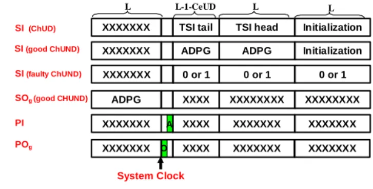
Figure 3 shows the C-ADPG pattern format. The initialization pattern is the first bit of TSI patterns replicated by L times. This initialization ensures that the head portion of the TSI pattern is shifted into the scan chain without being changed by faults. The head portion of the TSI pattern is then shifted in without observing any SO or PO. At this time, the sensitive bit is located at the most upstream scan cell. The ChUD is again shifted until the sensitive bit reaches the position of the CeUD. The number of shifts equals L – 1 minus the index of the CeUD. At this time, the sensitive bit is located at the CeUD. One primary input pattern is applied (A) and the corresponding primary outputs are observed (O). A system clock is pulsed to capture the responses into the scan chains. The scan outputs of good ChUNDs are observed; the scan outputs of the other chains are masked. To ensure only one sensitive bit at a time, all-zero patterns or all-one patterns are applied to faulty ChUNDs. On the contrary, the scan input patterns to the good ChUNDs can be specified by the C-ADPG.
SI (ChUD) TSI tail TSI head
PI POg XXXXXXX SOg (good CHUND) XXXX XXXXXXXX XXXXXXX L L XXXXXXX ADPG XXXX XXXX XXXXXXX O A Initialization XXXXXXXX XXXXXXX L L-1-CeUD XXXXXXX XXXXXXX ADPG ADPG XXXXXXX Initialization 0 or 1 0 or 1 XXXXXXX 0 or 1 System Clock SI (good ChUND) SI (faulty ChUND)
Figure 3. C-ADPG Pattern Format 2.) C-ADPG
cell that contains the sensitive bit, where S is opposite to the good value of the sensitive bit. In the case of single fault, the C-ADPG patterns can simply be generated by a regular combinational SSF ATPG tool because the contents of the ChUD are fully specified except the sensitive bit. In the presence of multiple faults, however, the actual contents of the ChUD are not fully specified because the number of flipped bits is unknown. To circumvent this problem, the TSI with unknown (TSIX) patterns is proposed for ADPG on a scan chain with multiple faults. The TSIX patterns are TSI patterns that have consecutive unknown values to the immediate upstream or downstream of the sensitive bits. TSIX patterns for the ST fault are denoted as TS01Xx or TS10Xx, in which x represents the number of unknown values.
TS01Xx and TS10Xx patterns have x unknown values in the upstream of the sensitive bit;
TH10Xx and TH01Xx patterns have x unknown values in the downstream of the sensitive
bit. TSIX patterns with x unknowns are used for a scan chain with (x+1) faults. With TSIX patterns, the C-ADPG can now be implemented by a regular combinational SSF ATPG tool. The C-ADPG steps as follows. (1) Right shift the TSIX pattern until the sensitive bit reaches the position of the CeUD in the head portion. Initialize the scan cells of the ChUD to the head portion of the shifted TSIX pattern. (2) Initialize the scan cells in faulty ChUNDs to all ones or zeros. (3) Inject a stuck-at S fault at the sensitive bit; S is opposite to the sensitive bit. (4) Run combinational SSF ATPG to detect the fault. Allow observation only at PO and SO of good ChUNDs. (5) If ATPG is successful, cell i is C-observable.
For a given fault type and a given number x, a cell is C-observable if C-ADPG succeeds using either the T01Xx or the T10Xx pattern; otherwise, it is C-unobservable.
Scan cells are C-unobservable for one of two possible reasons. The first is lack of propagation paths due to the constraints of TSI patterns. The second is the constraint that faulty ChUNDs are forced to all ones or all zeros. To enhance the diagnosis resolution, the C-unobservable cells must be diagnosed by the sequential diagnosis procedure (SDP).
B. S-ADPG
1.) Sequential Diagnosis Procedure, SDP
The SDP is different from the CPD in that the former has more than one system clock. The SDP steps are the following. (1) Initialize the ChUD by shifting in the first bit of the TSI pattern for L times. (2) Keep shifting in the TSI pattern until the sensitive bit reaches the CeUD. (3) Apply a primary input pattern. (4) Observe primary outputs (POa) and pulse a system clock. (5) Repeat steps 3 and 4 for a specified number of times. (6) Shift out the scan chains. Observe scan outputs of good ChUNDs. Mask scan outputs of the other chains.
In the first time frame, the TH10 pattern ‘11000’ is shifted into the chain and the sensitive bit is flipped by the HT fault in cell 2. The actual contents of scan cells become ‘11100’. After one system clock, the fault effect of the flipped sensitive bit is captured in cell 3 of the ChUD. The fault effect is then propagated from cell 3 to a primary output by applying PI2 =1. Note that, even though the fault effect is fedback to cell 2 in the second time frame, the S-ADPG is essentially a single fault (not multiple fault) sequential ATPG because the origin of the fault is uniquely generated by cell 2 in the first time frame.
1 1 4 3 2 1 0 0/1 PI1=0 0 0 fault detected at PO ChUD 0/1 0/1 ChUD 0/1 PI2=1 time frame #1 time frame #2
Figure 4. Fault in Cell 2 Detected by SDP (good/faulty) 2.) S-ADPG
The S-ADPG is similar to the sequential SSF ATPG and therefore can be implemented by existing tools with modifications. The S-ADPG includes even steps. (1) Right shift the TSIX pattern until the sensitive bit reaches the position of the CeUD in the head portion. Initialize the scan inputs of scan cells in the ChUD to the head portion of the shifted TSIX pattern. (2) Inject a stuck-at S fault at the scan input of the CeUD. S is opposite to the sensitive bit. (3) Initialize the scan inputs of all scan cells in faulty ChUNDs to all ones or zeros. (4) Assert the scan-enable signal (shift mode) and pulse one clock. By doing so, all the scan cells are initialized and the fault is injected into the CeUD. (5) De-assert the scan_enable (normal operation mode) and run sequential ATPG to detect the injected fault. Allow observation at the primary outputs only. (6) After the last system clock, observe scan outputs of good ChUNDs. Mask the scan outputs of the other chains. (7) If S-ADPG is successful, the CeUD is S-observable.
There is one major difference between the regular sequential SSF ATPG and the S-ADPG, the time frame that the stuck-at fault is present. The regular sequential SSF ATPG assumes that the stuck-at fault is present in every time frame; the S-ADPG assumes that the stuck-at fault is present only in the first time frame, not in any later time frame. This is because the scan cells are assumed to be faulty only in shift mode, not in normal operation mode. Based on this assumption, the fault is injected at the scan input, not the output, of the CeUD. Because the scan_enable is forced to zero after step 4, only the fault effects (not the stuck-at fault itself) remain in the
circuit after the first time frame.
3.) Diagnosis Resolution
A cell is observable if it is either C-observable or S-observable; otherwise, it is
unobservable. The diagnosis upper bound of cell i, DUB(i), is the index of the
nearest upstream observable cell of cell i (excluding cell i itself). The diagnosis
lower bound of cell i, DLB(i), is the index of the nearest downstream observable cell
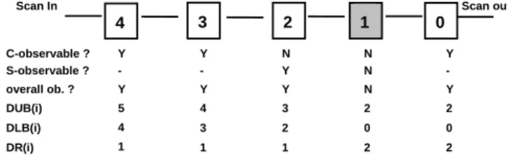
of cell i (including cell i itself). The diagnosis resolution of a cell i, DR(i), is equal to DUB(i) minus DLB(i). In Figure 5, cells 4, 3, and 0 are C-observable and the others are C-unobservable. After performing S-ADPG on cells 2 and cell 1, the former becomes S-observable. Overall, cells 4, 3, 2, 0 are observable and cell 1 is unobservable. 1 2 3 4 0 DUB(i) 5 4 3 2 2 3 2 0 0 1 1 2 2 4 1 DLB(i) DR(i) C-observable ? Y Y N N Y S-observable ? - - Y N - overall ob. ? Y Y Y N Y
Scan In Scan out
Figure 5. DUB, DLB, and DR C. Match
After testing the CUD on the ATE, the actually observed POa and SOa are compared with the good outputs, POg and SOg off line. The first mismatch cell is the most upstream cell in which a mismatch occurs. The first mismatch cell is obtained from either the CDP or the SDP, whichever is more upstream. The upper bound of the first fault, U(f1), and the lower bound of the first fault, L(f1), are the DUB and the
DLB of the first mismatch cell, respectively.
D. Experimental Results
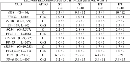
Table III shows the experimental results of the ISCAS’89 and ITC’99 benchmark circuits. A commercial tool that supports both combinational and sequential ATPG is used. The average DRs and the worst DRs are the average and the maximum DR(i) values among all scan cells in the ChUD. The first row (C) shows DRs obtained from the C-ADPG only. The second row (C+S) shows DRs obtained from the C-ADPG plus the S-ADPG. Three systems clocks are applied in the S-ADPG. The total numbers of combinational logic gates (G), the total number of flip-flops (FF), and ChUD length (L) are shown for reference. Flip-flops in the ISCAS and the ITC circuits are evenly stitched into two and sixteen scan chains, respectively. The experimental data show that worst DRs are better than fifteen, even in the presence of eleven faults (X=10). For comparison, the worst DR of a previous single HT fault diagnosis is 27 on an industry design (G=430K, FF=22K, L=410) [12]. In addition to good diagnosis resolutions, our diagnosis pattern is much shorter than regular ATPG patterns. For the case of B19, only 409 patterns, instead of 10K regular ATPG
patterns, are needed for diagnosis.
TABLE III
DIAGNOSIS RESOLUTIONS OF ST AND HTFAULTS (AVERAGE/WORST)
CUD ADPG ST X=0 ST X=10 HT X=0 HT X=10 s838 (G=446; C 3.3 / 4 9.4 / 12 3.3 / 4 10 / 12 FF=32; L=16) C+S 1.0 / 1 1.0 / 1 1.0 / 1 1.0 / 1 s5378 (G=2,779; C 1.8 / 6 2.5 / 9 1.8 / 6 2.2 / 7 FF= 179; L=90) C+S 1.2 / 3 1.5 / 4 1.2 / 3 1.5 / 4 s9234 (G=5,597; C 2.2 / 5 2.8 / 8 2.2 / 5 2.9 / 9 FF=211; L=106) C+S 1.1 / 3 1.2 / 3 1.1 / 3 1.2 / 3 s15850 (G=9,772; C 1.7 / 4 1.7 / 4 1.7 / 4 1.7 / 4 FF=534; L=267) C+S 1.0 / 2 1.0 / 2 1.0 / 2 1.0 / 2 s38584 (G=19,253; C 1.7 / 6 1.7 / 6 1.7 / 6 1.7 / 6 FF=1,426; L=713) C+S 1.0 / 2 1.0 / 2 1.0 / 2 1.0 / 2 B19 (G=230K; C 6.5 / 19 7.9 / 20 6.4 / 19 8/ 21 FF=6.6K; L=409) C+S 3.2 / 9 5.4 / 15 3.4 / 11 5.6 / 15
Table IV shows DRs of one, two, and three system clocks (HT fault, X=10). The CPU time is measured on a SUN Blade 2500 workstation with 8GB memory. The DRs of C-ADGP, which can be regarded as one SCK, are shown in the first column. As the number of system clock increases, DRs improve at the cost of CPU time. The B19 S-ADPG with three system clocks is finished within one hour of CPU time, demonstrating the feasibility of the technique on large designs. The S-ADPG experiment on B19 has no abort or memory problem. (See discussion for the sequential ATPG details.) The number of system clocks needed in the S-ADPG is dependent on the sequential depth of the CUD. The sequential depth of a circuit represents the maximum level of flip-flops that a fault effect must propagate through before reaching observation points [14].
TABLE IV
DRS AND CPUTIME OF DIFFERENT SYSTEM CLOCKS (X=10,HT)
CUD 1SCK (C-ADPG) 2SCK 3SCK DR (A/W) CPU (Sec.) DR CPU DR CPU s838 9.4 / 12 0.0 1.0 / 1 1.3 1.0 / 1 1.6 s5378 2.5 / 9 0.2 1.6/ 4 4.4 1.5 / 4 6.7 s9234 2.8 / 8 0.4 1.2 / 3 19.1 1.2 / 3 35.5 s15850 1.7 / 4 2.1 1.0 / 2 49.7 1.0 / 2 73.2 s38584 1.7 / 6 14.6 1.0 / 2 213.9 1.0 / 2 238.4 B19 8.0 / 21 54.6 6.1 / 17 2,940.0 5.6 / 15 3,265.0 REFERENCES
[1] Y. Wu, “Diagnosis of Scan Chain Failures,” Int’l Symp. On Defect and
Fault Tolerance in VLSI systems, pp. 217-222, 1998.
[2] Y. Huang, W.-T. Cheng, S. M. Reddy, C.-J. Hsieh, and Y.-T. Hung, “Statistical Diagnosis for Intermittent Scan Chain Hold-Time Fault,” Proc.
IEEE Int’l Test Conf., pp. 319-327, 2003.
[3] R. Guo, and S. Venkataranman , “A New Technique for Scan Chain Failure Diagnosis,” Proc. Int’l Symp. Testing and Failure Analysis, pp. 723-732, 2002.
[4] B. Kruseman, A. Majhi, C. Hora, S. Eichenberger, J. Meirlevede, “Systematic Defects in Deep Sub-Micron Technologies,” Proc. IEEE Int’l. Test Conf., pp. 290-298, 2004.
[5] F. Motika, P. Nigh, P. Song, and H. B. Druckerman, “AC Scan Diagnostic Method,“ U.S. Patent 6,516,432 B1, Feb. 4, 2003.
[6] J. Schafer, F. Policastri and R Mcnulty, “Partner SRLs for Improved Shift Register Diagnostics,” Proc. IEEE VLSI Test Symp., pp. 198-201, 1992. [7] S. Edirisooriya, and G. Edirisooriya, “Diagnosis of Scan Path Failures,”
Proc. IEEE VLSI Test Symp., pp. 250-255, 1995.
[8] S. Narayanan and A. Das, “An Efficient Scheme to Diagnose Scan Chains,” Proc. Int’l Test Conf., pp.704-713, 1997.
[9] S. Kundu, “Diagnosis Scan Chain Faults,” IEEE Trans. VLSI Syst., pp. 512-516, 1994.
[10] J. Hirase, N. Shindou, and K. Akahori, “Scan Chain Diagnosis Using IDDQ Current Measurement,” Proc. Asian Test Symp. pp. 153-157, 1999. [11] K. Stanley, “High-Accuracy Flush-and-scan Software Diagnostic,” IEEE Des.
Test. Comput., pp. 56-62, Nov-Dec, 2001.
[12] R. Guo, and S. Venkataranman, “A Technique for Fault Diagnosis of Defects in Scan Chains,” Proc. IEEE Int’l Test Conf., pp. 268-277, 2001. [13] P. High, D. Vallett, A. Patel and et. al., “Failure Analysis of Timing and IDDq
Failures from the SEMATECH Test Methods Experiment,“ Proc. IEEE Int’l.
Test Conf., pp.43-52 , 1998.
[14] M. L. Bushnell and V. D. Agrawal, Essentials of Electronic Testing for
Digital, Memory and Mixed-signal VLSI Circuits, p. 226, Boston: Kluwer
Academic Publishers, 2000.
[15] Synopsys, TetraMAX ATGP User Guide, V-2003.12, Dec. 2003. I.