SYMMETRIC AND PROGRAMMABLE
PROTOTYPING SYSTEM
MULTI-CHIP MODULE FOR RAPID
Mao-Hsu Yen', Sao-Jie Chen' and Sanko H. Lan'
'Department of Electronic Engineering Taipei, Taiwan, R.O.C.
*Department of Electrical Engineering National Taiwan University of Science and Technology National Taiwan University
Taipei, Taiwan, R.O.C.
Abstract
-
T o accelerate prototyping designs, we propose a new Sym- metric and Programmable MCM (SPMCM) substrate, which consists of 'a symmetrical array of slots for bare-chip attachment and Field Pro- grammable Interconnect Chips (FPICs) for substrate routing. Especial- ly, the F P I C that we developed contains two kinds of polygonal routing modules and some virtual-wires t o reduce the number of routing switches and pin count. For a bare-chip slot with 2n pads, the number of switches used in the polygonal routing module is less than the conventional rout- ing module by m J 4times, where the flexibility ratio T F ~ is close t o1.
INTRODUCTION
MCM packaging technology used in electronic systems translate the semi- conductor speed into system performance [1]-[3] ] but high-density and high- performance MCMs are expensive to fabricate and usually requires weeks of engineering effort for prototyping designs and consumer product verification. The engineering delay in designing and fabricating such MCMs become u- nacceptable in today's competitive market. The needs of quick turnaround time, high product yield, and low cost have led to the development of an- other approach] called Symmetric and Programmable Multi-Chip Module (SPMCM) [4]-[6]. The SPMCM technology provides the designers with a pre-characterized MCM substrate and some programmable interconnections such that they can generate a fast prototyping or a final consumer product in a short time.
Several systems have been proposed for the rapid-prototyping design [7]- [12], most of them interconnect the Field Programmable Gate Arrays (FP- GAS) with some Field Programmable Interconnect Chips (FPICs) [13]-[16] on a substrate board. For instance, the BORG [7],, [8] system is
a
reconfigurable prototyping board for FPGAs based on the Clos network. Galloway et al. (91 proposed a reconfigurable system, called Transmorgrifer-2, which is a hierar- chical design based on the I-CUBE [14] routing chip. The Field ProgrammableMulti-Chip Module (FPMCM) [lo] system is a reconfigurable system combin- ing both the state-of-art FPGA and MCM technologies. Thomae and Bout [ll] devised a multi-FPGA board for rapid prototyping, in which the ring architecture is used to interconnect FPGAs. A board for logic emulation has been developed by Babb et al. at MIT [12], which uses virtual-wires technique t o overcome the pin count limitations. From the above existing reconfigurable systems [7]-[12], we observe that most of the efforts have been spent on de- signing a flexible interconnection architecture to mitigate the pin limitation. In order to improve the foregoing problem, we propose an SPMCM struc- ture, which consists mainly of a symmetrical array of bare-chip slots surround- ed with some FPICs for slot interconnections. The bare-chip slots allow bare chips from different manufacturing processes to attach on the MCM substrate; therefore, our architecture is more flexible and can be used t o realize a rapid prototyping containing bare-chips of various technologies. Our proposed FPIC architecture uses polygonal routing modules and virtual-wires [ 121 technique to reduce the requirements of programmable switches and pin count. Since this architecture spends less hardware cost and has a regular structure, it is suitable for VLSI implementation. Moreover, cascading the architecture can scale up the routing resources. This paper focuses on the design of efficient FPICs and the structure of a flexible bare-chip slot in an SPMCM.
SPMCM ARCHITECTURE
Our SPMCM is a programmable MCM substrate [4]-[6] that consists of an array of bare-chip slots and interconnection FPICs [13]-[16] on an MCM substrate, as shown in Fig. 1. The MCM substrate and FPICs are pre- fabricated in large volume and well tested. On the MCM substrate, parts of the pads are designed for the FPICs; the others are for the commercial or customized bare chips attached to the bare-chip slots. The FPICs are attached to the MCM substrate using flip-chip bounding technology, while bare-chips using wiring bounding technology. Thus, these bare chips attached on the SPMCM can be manufactured with different processes. On the substrate, each bare-chip pad is connected via a substrate metal wire to one of the FPIC pads, and net routing is accomplished by programming the routing modules in FPICs.
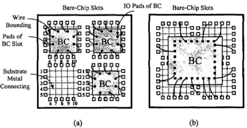
The purpose of these flexible bare-chip slots is aimed at attaching bare chips on an SPMCM in different combinations. Figures 2(a) and 2(b) show two different usage of our four-slot structure. In each of the bare-chip slots, each pair of horizontal (or vertical) pads is connected together through substrate metal wiring. We can have four small bare chips attached to the four small bare-chip slots, as shown in Fig. 2(a), or a large bare chip occupying all the four slots, as shown in Fig. 2(b).
Fig. 1: SPMCM architecture.
Bare-Chip Slots 10
-
Pads ofBc
Bare-Chip Slots Wire-
Bounding Pads of-
BC Slot Substrate-
Metal ConnectingFig. 2: Bare-chip slots structure; (a) Attached with several small bare chips, and (b) Attached with a large bare chip.
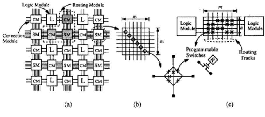
Our SPMCM approach is similar to the symmetric FPGA approach [17]- [19]. First, a brief review of the symmetric FPGA architecture is described as follows. A typical symmetric FPGA consists of an array of logic modules that can be connected by general routing resources, as shown in Fig. 3(a). The routing resources comprise metal wires and routing modules. A rout- ing module (RM) consists of two connection-modules (CMs) connected to a switch-module (SM), which contain many programmable switches, as shown in Fig. 3(a). The logic-module (L) resources contain configurable digital circuits that implement logic functions.
Similar to the symmetric FPGA model shown in.Fig. 3(a), if we substitute the logic modules with the bare-chip slots and each of the routing modules with an FPIC, we obtain an SPMCM system, as shown in Fig. 1. In this manner, the routing algorithm and architecture of the SPMCM are similar to the symmetric FPGA [18]. Therefore, we use the terms "routing module" and "FPIC" interchangeably in this paper. In the following sections, we will first indicate that the conventional routing module presents an obstacle to the implementation of an FPIC in terms of the number of programmable switches. Thus, we propose a polygonal routing module architecture to minimize the number of programmable switches.
CONVENTIONAL AND POLYGONAL ROUTING
MODULES
Conventional routing module
In a conventional symmetric FPGA, the switch module is a 4-sided block, denoted as SM(4, m ) , where m is the number of terminals on each side of the switch module
,
as shown in Fig. 3(b). Let the flexibility of a switch module beFs
[17], which is used to represent the number of programmable switches connecting one terminal to Fs terminals on the other three sides of a switch module. For example, the conventional switch module has Fs = 3, then a switch module SM(4, m ) would contain 6m programmable switches.A connection module, denoted as C M ( m , n ) , is an m x n rectangular block,
where m is the number of tracks connected to the switch modules, and n is the number of tracks connected to the bare-chip slots (logic modules), as shown in Fig. 3(c). Therefore, each bare-chip slot can have at most 2n pads. A conventional routing module consisting of two connection modules C M ( m , n )
and a switch module SM(4, m ) , is denoted as RM(4, m, n ) , as shown in Fig. 3(a). The flexibility of a connection module [17], F c , is defined as the num- ber of tracks to which each pad in a bare-chip slot (logic module) can be connected, for example as shown in Fig. 3(c) F c = 4. Thereafter, a con-
Connec
Module
m
Fig. 3: (a) A typical symmetric FPGA model and routing module RM(4, m , n); (b) Switch module S M ( 4 , m); and (c) Connection module C M ( m , n ) . Fc = 4, FS = 3, m = 6, n = 4, and T F ~ = 416.
nection module can contain Fc x n programmable switches. In a connection module C M ( m , n ) , the ratio of the Fc to m is called the flexibility ratio and
T F ~ = F c / m . The T F ~ is the probability that a wire arriving a t a particular
track in the connection module is able to connect to the required pin of a bare-chip slot (logic module) [17], thus 0
5
T F ~5
1. Rose and Brown [17]suggested that Fs=3 and a high value of Fc, i.e. rpc close to 1, are sufficient to provide high routability in a symmetric FPGA.
Number of switches in a conventional routing module
Let the number of programmable switches in an RM(4, m , n ) be denoted as P S ( 4 , m , n ) . Thus the P S ( 4 , m , n ) is equal to the number of programmable switches between the two C M ( m , n ) and an S M ( 4 , m ) . These are given byP S ( 4 , m , n ) = 2Fcn
+
6m = 2 r ~ ~ m n+
6m = 2 r n ( r ~ , n+
3) (1) In Equation ( l ) , normally, m is proportional to n and T F ~ is close to 1.WhenrFcn
>>
3, P S ( 4 , m , n ) isproportionalton2. Ifweusean R M ( 4 , m , n ) to fabricate an FPIC for the inter-bare-chip routing in an SPMCM, the value of P S ( 4 , m l n ) becomes very large, for n is usually large. This presents an obstacle to the VLSI implementation of an RM(4, m , n ) FPIC.Polygonal routing module
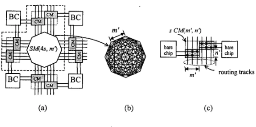
Based on the conventional routing module RM(4, m , n ) , as shown in Fig. 3(a), we can divide each connection module C M ( m , n) into s smaller connec-
s CM(m', n')
Fig. 4: (a) Polygonal routing module R M ( 4 s , m', n'); (b) Polygonal switch module S M ( 4 s , m'); and (c) Connection module C M ( m ' , n'). Fc' = 2, Fs' = 7, m' = 3, n' = 2 , T F c ' = 213 = r F c , and s = 2.
tion modules C M ( m ' , n ' ) such that each C M ( m ' , n ' ) is connected to one of the 4s sides of the polygonal switch module, as shown in Fig. 4(a), where m = s x m', n = s x n', FC = s x Fc', Fc and Fc' are the flexibilities of
C M ( m , n ) and C M ( m ' , n'), respectively. The polygonal switch module [19] is a 4s-side block, denoted as S M ( 4 s , m ' ) , where m' is the number of ter- minals on each side of the polygonal switch module, as shown in Fig. 4(b). Furthermore, a terminal in one side can be connected to a terminal in one of the other (4s - 1) sides of the SM(4s,m') through programmable switches, thus the flexibility F , ' of an S M ( 4 s , m ' ) is equal to (4s - 1). Compared with the conventional routing module, a polygonal routing module RM(4.5, m', n')
comprises 2s smaller connection modules C M ( m ' , n') interconnected by a 4s- side switch module SM(4s,m'), as shown in Fig. 4(a).
Number
of switches in a polygonal routing module
Since the number of switches in 2s connection modules C M ( m ' , n ' ) is equal to 2sFc'n', and the number of switches'in a polygonal switch moduleSM(4.5, m') is equal to m'((4s
-
1)+
(4s - 2 )+
. . .
+
1). Denote the number of switches in an RM(4s, m', n') as PS(4s, m', n ' ) . By summing the number of switches in all the above modules, we have:PS(4s, m', n') = 2sFc'n'
+
2m's(4s - 1) (2) We indicate that the function PS(4s,m',n') has minimum value at s =m / 2 ,
That is to say, the flexibilities Fc' = F c / s and Fs' = 4s - 1 determined by s = m / 2 minimize P S ( 4 s , m ' , n ' ) . According to Equation (1), m is proportional to n. When rF,n
>>
1, P S ( 2 m , m ' , n ' ) is proportional to n3/2 by Equation (3). Dividing Equation (1) by Equation (3) yields:2 m ( r ~ , n + 3 ) - r ~ , n + 3 -
P S ( 4 , m , n ) - -
P S ( 2 m , m', n') 2m(4-
-
1) 4- - 1 Now if rF,n>>
3, then Equation (4) will becomerF,n -
m
%--- PS(4, m , n ) P S ( 2 m , m m ' , n ' ) 4- 4 (4) (5)Equation (5) tells that when rF,n
>>
3, PS(4s,rn',n') at s =is less than P S ( 4 , m , n ) by m / 4 times. Thus, our proposed polygonal routing module could enlarge the practicability of implementing the FPIC in the SPMCM system.
VLSI CHIP IMPLEMENTATION OF THE FPIC
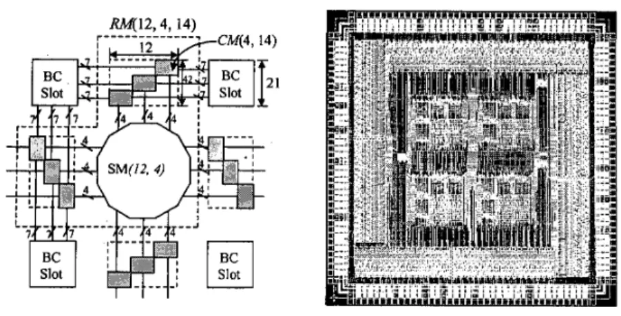
In Figs. 1 and 3(a), the polygonal routing module shown there has pa- rameters n = 42 and r~~ = l . Therefore, each bare-chip slot has 84.(2n) pads to connect to the FPIC in our SPMCM system. From Equation (3), the important value s of an RM(4s, m', n') can be obtained as follows: s =
-12 =
d-12
= 3.24. Let s = 3, then n' = n / s = 4213 = 14. Thus, our FPIC uses an RM(12,2k, 14), where k = 2, and is packaged as a 166-pin CQFP. An RM(12,4,14) polygonal routing module is shown in Fig. 5. Note that, its PS(12,4,14) = 600 is less than the convention- al PS(4,12,42) = 1080. Virtual-wires [12] technology is used in our FPIC to improve the routing resources and to overcome the pin count limitation by intelligently multiplexing each physical wire among multiple logical wires. The FPIC VLSI implementation combine four RM(12,4,14)'s and intelligent multiplexing. The chip layout is shown in Fig. 6 and it will be fabricated in a0.6prn Single-Poly-Triple-Metal CMOS technology through the Chip Imple- mentation Center (CIC), National Science Council, R.O.C. its performance data is summarized in Table 1. As mentioned above, this chip architecture is highly scalable, uses less programmable switches, and has lower pin count. Thus it is very suitable for VLSI implementation.
CONCLUSIONS
An area-efficient and flexible Symmetric and Programmable MCM (SPM- CM) has been described, and a symmetric-array FPIC VLSI architecture was proposed for the substrate routing between the bare-chip slots. This FPIC
RM(12,4, 14)
Fig. 5 : A polygonal routing module RM(8,6,21) architecture.
Fig. 6: Chip layout of the FPIC.
Table 1: Performance data.
architecture consists
of
four polygonal routing modules and intelligent mul- tiplexing structures, which can significantly reduce the requirements of pro- grammable switches number and pin count compared with the conventional routing module. We have implemented this VLSI architecture in a 0.6 p mCMOS technique to verify the function of our proposed SPMCM. In addition, this VLSI routing chip architecture can be easily scaled up with the routing resources. With its field programmable MCM substrate, our SPMCM can be used for implementing various prototyping designs based on user requirements without going through the foundry facility. The advantages are that the field programmable technology can reduce product development cycle and NRE (Non-Recurrence Engineering) cost, while MCM technology can achieve low power and small size.
ACKNOWLEDGMENTS
This work was partly supported by the National Science Council, ROC, under Grant NSC-86-2221-E-011-021.
References
[l] R. Johnson, ”Multichip Modules: Next-Generation Packages,” IEEE Spectrum, pp. 34-48, Mar. 1990.
[2] A. Iqbal, M. Swaminathan, M. Nealon, and A. Omer, ”Design tradeoffs among MCM-C, MCM-D and MCM-D/C technologies,” IEEE Transac- tions on Components, Packaging, and Manufacturing- Part B: Advanced Packaging, vol. 17, no. 1, pp. 22-29, Feb. 1994.
[3] R. C. Frye, ”Physical Scaling and Interconnection Delays in Mul- tichip Modules,” IEEE Transactions on Components, Packaging, and
Manufacturing-Part B: Advanced Packaging, vol. 17, no. 1, pp. 30-37, Feb. 1994.
[4] ,4. Dobbelare, El Gamal, D. How, and B. Kleveland, ”Field pro- grammable MCM system-design of an interconnection frame,” Proceed- ings of the IEEE 1992 Custom Integrated Circuits Conference, pp. 15.1/1-
6.
[5] S. Burman and Naveed A. Sherwani, ”Programmable Multichip Module,’’
IEEE Micro, pp. 28-35, April 1993.
[6] Lan S., ”Architecture and CAD Tools For a Field Programmable Multi- Chip Module,” Ph.
D.
Thesis, Stanford University, August 1995.[7] P. K. Chan., M. Schlag and M. Martin, ”BORG: A reconfigurable proto- typing board using field-programmable gate arrays,” Proceedings of the 1st international ACM/SIGDA Workshop on Filed-Programmable Gate Arrays, pp. 47-51, 1992.
[8] P. K. Chan. and M. Schlag, ”Architecture tradeoffs in field programmable device-based computing systems,” IEEE workshop on FPGAs for Custom Computing Machines, pp. 152-161, 1993.
[9] D. Galloway, D. Karchmer, P. Chow, D. Lewis, J. Rose, ”The Transmo- grifier: The university of Toronto field-programmable system,’’ Second
Canadian Workshop on Field-Programmable Devices, 1994.
[lo] J. Darnauer, P. Garay, T. Isshiki, J . Ramirez, W. W. -M. Dai, ”A Field Programmable Multi-Chip Module (FPMCM)
,”
IEEE Workshop on FPGAs for Custom Computing Machines, pp. 1-10, 1994.[ll] D. A. Thomae and Van Den Bout, ”Automatic circuit partitioning in the Anyboard rapid prototyping system,” Microprocessors and Microsystem- S, pp. 283-90, 1992.
[12] J. Babb, R. Tessier, and A. Agarwal, ”Virtual Wires: Overcoming Pin Limitations in FPGA-based Logic Emulators,” IEEE Workshop on FP-
GAS for Custom Computing Machines, pp. 142-151, 1993.
[13] Mao-Hsu Yen, Mon-Chau Shie, and Sanko H. Lan, ”Polygonal routing network for FPGA/FPIC” at 1999 International Symposium on VLSI
Technology, System, and Applications, 1999 VLSI-TSA.
[14] I-Cube, Inc., ”I-Cube FPID family data book,” November 1993. [15] Aptix, Inc. ” Aptix filed programmable interconnect data book,” 1993
[16]
R.
Guo, H. Nguyen,A.
Srinivasan, H. Verheyen, H. Cai, S. Law, and A. Mohsen, ”A 1024 Pin Universal Interconnection Array with Routing Ar- chitecture,” in Proc. IEEE 1992 Custom Integrated Circuits Conference,pp, 4.5.1-4.5.4.
,
May 1992.(171 J . Rose and S. Brown, ”Flexibility of interconnection structures for field- programmable gate arrays,” IEEE J. Solid State Circuits, vol. 26, no. 3,
pp. 277-282, March 1991.
[18] Y. Sun,
T.
C. Wang,C.
K. Wong, andC. L.
Liu, ”Routing for symmetric FPGAs and FPICs,” Proc. IEEE Trans. Computer Aided Design, vol. 16,no. 1, pp. 20-31, Jan. 1997.
[19] G-M Wu, M. Shyu, and Y-W Chang, ”Universal switch blocks for three- dimensional FPGA Design,’’ at 1999 ACM International Symposium on Field Programmable Gate Arrays, (FPGA-99).