Reduction of photoleakage current in polycrystalline silicon thin-film transistor using N
H 3 plasma treatment on buffer layer
Hau-Yan Lu, Ting-Chang Chang, Po-Tsun Liu, Hung-Wei Li, Chin-Wei Hu, Kun-Chin Lin, Chao-Chun Wang, Ya-Hsiang Tai, and Sien Chi
Citation: Applied Physics Letters 92, 153507 (2008); doi: 10.1063/1.2912026 View online: http://dx.doi.org/10.1063/1.2912026
View Table of Contents: http://scitation.aip.org/content/aip/journal/apl/92/15?ver=pdfcov
Published by the AIP Publishing
Articles you may be interested in
Effect of double-sided Ca Ti O 3 buffer layers on the electrical properties of Ca Cu 3 Ti 4 O 12 films on Pt Ti Si O 2 Si substrates
J. Appl. Phys. 100, 104101 (2006); 10.1063/1.2374952
Hydrogen resistive double-side ( Pb 0.72 La 0.28 ) Ti 0.93 O 3 buffered Pb ( Zr 0.52 Ti 0.48 ) O 3 thin films
J. Appl. Phys. 100, 024107 (2006); 10.1063/1.2216435
Characteristics of metal-ferroelectric-insulator-silicon structures with ferroelectric ( Pb 0.8 Ba 0.2 ) Zr O 3 thin films and ( Ba 0.5 Sr 0.5 ) Ti O 3 buffer layer
Appl. Phys. Lett. 88, 122901 (2006); 10.1063/1.2186103
Passivation effects on the stability of pentacene thin-film transistors with SnO 2 prepared by ion-beam-assisted deposition
J. Vac. Sci. Technol. B 23, 2357 (2005); 10.1116/1.2102969
Effect of double-sided ( Pb 0.72 La 0.28 ) Ti 0.93 O 3 buffer layers on the ferroelectric properties of Pb ( Zr 0.52 Ti 0.48 ) O 3 thin films
Appl. Phys. Lett. 86, 032903 (2005); 10.1063/1.1852086
This article is copyrighted as indicated in the article. Reuse of AIP content is subject to the terms at: http://scitation.aip.org/termsconditions. Downloaded to IP: 140.113.38.11 On: Wed, 30 Apr 2014 23:07:35
Reduction of photoleakage current in polycrystalline silicon thin-film
transistor using NH
3plasma treatment on buffer layer
Hau-Yan Lu,1 Ting-Chang Chang,2,a兲 Po-Tsun Liu,3 Hung-Wei Li,1 Chin-Wei Hu,4 Kun-Chin Lin,4Chao-Chun Wang,1Ya-Hsiang Tai,3and Sien Chi1
1
Department of Photonics & Institute of Electro-Optical Engineering, National Chiao Tung University, Hsinchu, Taiwan 300, Republic of China
2
Department of Physics and Institute of Electro-Optical Engineering, Center for Nanoscience and Nanotechnology, National Sun Yat-sen University, 70 Lien-hai Road, Kaohsiung 804, Taiwan, Republic of China
3
Department of Photonics and Display Institute, National Chiao Tung University, 1001 Ta-Hsueh Rd., Hsinchu, Taiwan 300, Republic of China
4
LTPS Array Process Department, AU Optronics Corporation, Hsinchu, Taiwan 300, Republic of China 共Received 20 January 2008; accepted 31 March 2008; published online 15 April 2008兲
The technology of polycrystalline silicon thin-film transistors共poly-Si TFTs兲 with low photoleakage current is developed in this work. The electrical characteristics of poly-Si TFTs under illumination were significantly improved employing the NH3plasma treatment on the buffer layer, with no need for complicate device structure and additional masks. The trap states that originated from the plasma bombardment on the interface between the poly-Si layer and buffer oxide can effectively recombine the light-induced electron-hole pairs. The fewer residual electron-hole pairs lead to the lower photoleakage current and improved subthreshold swing, as well as maintaining good electrical characteristics in the dark sate. © 2008 American Institute of Physics.关DOI:10.1063/1.2912026兴
Polycrystalline silicon thin-film transistors 共poly-Si TFTs兲 have been widely used in active matrix liquid crystal displays共AMLCDs兲 and active matrix organic light-emitting diode display.1–3 The poly-Si TFTs offer great potential for active matrix display technology because of their superior electrical characteristics over those of amorphous silicon TFTs共a-Si TFTs兲. Recently, the demand of high-end mobile electronic products, such as digital camera, cell phone, and mobile TV, is continuing to rapidly grow, and so the high resolution and high image quality becomes the critical issue in the development of mobile displays. Therefore, the bright-ness of back light is getting higher and higher to meet the requirement for fine image quality and superior readability as people use these mobile electronic products under sunlight outdoors.4,5However, poly-Si TFTs usually suffer from un-desirable photoleakage current under a high illumination environment.6 The high leakage current and increased sub-threshold swing共SS兲 of poly-Si TFT under illumination in AMLCDs should be reduced to avoid losing the charges stored in pixels. Therefore, the voltages that are held across the pixel electrodes would be diminished to affect the gray level controlling, which in turn, would cause a low contrast ratio and error color display. However, the researches about improving the electrical characteristics in poly-Si TFTs under illumination are very few and the mechanism of photoleak-age current in poly-Si TFT is still not clarified.
In this work, without complicated device structure or process steps, a simple method to reduce the photoleakage current of poly-TFTs has been developed. The surface of buffer layer in the proposed poly-Si TFT is treated employ-ing the NH3 plasma to lower the photoleakage current and improve the SS characteristics under back-light illumination with the original characteristics of poly-Si TFTs
Top-gate p-type poly-Si TFTs with lightly doped drain 共LDD兲 were fabricated in this letter. First of all, a 50-nm-thick SiNx and a 150-nm-thick SiO2 films were se-quentially deposited to form buffer layer by plasma enhanced chemical vapor deposition 共PECVD兲. Then, the surface of buffer layer was treated employing NH3plasma for 10 min. A thin 50-nm-thick undoped a-Si film was deposited by PECVD at 380 ° C, followed by dehydrogenated via furnace annealing process at 450 ° C. The a-Si films were crystal-lized by 308 nm XeCl excimer laser with the line-shaped beam power of 350 mJ/cm2. The 100-nm-thick gate insula-tor was deposited by tetraethyl orthosilicate base oxide. The source/drain and LDD region were formed by the mass-separated ion implanter technique. The doping activation was performed by rapid thermal anneal irradiation. MoW was sputtered as a gate metal. The dimensions of TFTs in this work were the following: channel length共L兲 6m, channel width共W兲 6m, and the LDD length 1m.
Figure1shows the ID-VGtransfer curves of conventional
p-channel poly-Si TFT operated in linear region under the
dark and photostates. The brightness of back light for photo-state measurement is set as 3100 nit. As the gate bias is swept from 0 to 12 V, the leakage current of poly-Si TFTs in the dark state was about 10−13A. With the same range of gate bias, the leakage current of poly-Si TFT under illumi-nation is as high as two orders of magnitude, around 10−11A. In addition, the SS is increased under illumination, about 0.45 V/decade, as the initial value in dark is 0.29 V/decade. The variation of SS is about 55%. The on/off current ratio of poly-Si TFTs was substantially reduced due to the high photoleakage current, so that the function of TFTs used as the pixel switch under illumination would be seri-ously affected.
Since the light emitted from the back light is mainly absorbed at the interface between the poly-Si layer and the
a兲Electronic mail: [email protected].
APPLIED PHYSICS LETTERS 92, 153507共2008兲
0003-6951/2008/92共15兲/153507/3/$23.00 92, 153507-1 © 2008 American Institute of Physics
This article is copyrighted as indicated in the article. Reuse of AIP content is subject to the terms at: http://scitation.aip.org/termsconditions. Downloaded to IP: 140.113.38.11 On: Wed, 30 Apr 2014 23:07:35
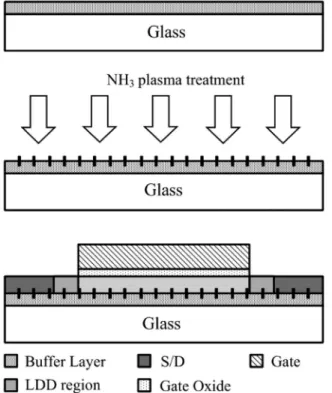
buffer layer, plenty of electron-hole pairs are generated in the bottom of poly-Si film.7Furthermore, the energy-band struc-ture of Si material has indirect bandgap. The excess electron-hole pairs induced by the absorption of light would not be directly recombined from band to band due to the momen-tum conservation principle. The numerous electron-hole pairs are accumulated in the bottom of poly-Si layer. It fol-lows that the excess holes flow to the drain under the nega-tive drain bias for p-channel devices, generating the photo-leakage current. To release the issue, the trap states on the surface of the buffer layer were induced by the NH3plasma treatment to assist the recombination of excess electron-hole pairs. Figure 2 plots the key process flow of proposed poly-Si TFTs. The surface quality in the top SiO2 film of buffer layer would be degraded to generate the surface trap
density employing the NH3 plasma bombardment. After plasma treatment, the process flow is the same as the stan-dard one.
Figure 3 shows the transfer curves of the conventional and proposed TFTs. The electrical characteristics of poly-Si TFTs with NH3 plasma treatment on the buffer layer are almost entirely identical to the conventional ones. It is veri-fied that the crystallization status of poly-Si would not be affected by the surface states of buffer layer. Therefore, the proposed method can be completely compatible with the conventional poly-Si process. Furthermore, in order to con-firm the uniformity of poly-Si TFTs with proposed method, the average of key parameters extracted at linear operation in 12 TFTs with various location of substrate are summarized in the inset table of Fig. 3. It is found that the uniformity of proposed poly-Si TFTs kept in a good condition and the key parameters were nearly unchanged in comparison with the conventional devices.
The photoleakage current of the conventional and the proposed devices, which is extracted at a voltage兩VG-Vt兩 of
7 V as VDis 0.1 V, with the increasing brightness of back
light共2160, 3100, 4110, and 5620 nit兲 are illustrated in Fig.
4共a兲. The photoleakage current of conventional poly-Si TFTs substantially increases with increasing brightness of back light. In contrast, for proposed device, the leakage current under illumination is slightly increased and there remains a weak dependence of the brightness of back light. The maxi-mum of photoleakage current in the TFT with NH3 plasma treatment is 8.1 pA. It is still much lower than 13.6 pA, the minimum of that in conventional TFT. Figure4共b兲shows the comparison of SS in the conventional and proposed TFTs under illumination with increasing brightness. The increasing ratio of SS, ⌬SS, is defined as 共SSphoto/SSdark− 1兲, where SSphoto and SSdarkare the SS of devices at drain voltage of −0.1 V under photo and dark states. As the brightness of back light is 5610 nit, the maximum⌬SS of the conventional and proposed TFT are 46.4% and 85.3%, respectively. The significant improvement of variation in SS of poly-Si TFT under illumination is confirmed.
FIG. 1. ID-VGcurves of the conventional poly-Si TFT operated in the linear region under illumination and dark states. A significantly increase of leakage current was found.
FIG. 2. The proposed process diagram for treating the surface of buffer layer using NH3plasma bombardment. Numerous state densities are gener-ated to be taken as the recombination center for light-induced electron-hole pairs.
FIG. 3. The comparison of electrical characteristics in conventional and proposed TFT under dark state.
153507-2 Lu et al. Appl. Phys. Lett. 92, 153507共2008兲
This article is copyrighted as indicated in the article. Reuse of AIP content is subject to the terms at: http://scitation.aip.org/termsconditions. Downloaded to IP: 140.113.38.11 On: Wed, 30 Apr 2014 23:07:35
In conclusion, we have demonstrated a simple method to fabricate the poly-Si TFT with low photoleakage current without changing the structure or process flow. The proposed poly-Si TFT exhibits the impressively low leakage current and improved SS under illumination. The uniformity and electrical characteristics of proposed devices are almost same as the conventional ones. As the brightness of back light is set to 5610 nit, the photoleakage and the variation of SS in proposed TFT are 8.1 pA and 46.3%, respectively while those in conventional TFT are 35.6 pA and 85.3%.
This work was supported by MOE ATU Program, the National Science Council, Taiwan, R.O.C., under Contract No. NSC-96-2120-M-110-001, and partially supported by MOEA Technology Development for Academia Project No.
94-EC-17-A-07-S1-046. The authors would like to thank AU Optronics Corporation共AUO兲 for their technical support.
1H. Kuriyama, S. Kiyama, S. Noguchi, T. Kuahara, S. Ishida, T. Nohda, K. Sano, H. Iwata, S. Tsuda, and S. Nakano, Tech. Dig. - Int. Electron De-vices Meet. 1991, 563.
2S. W. B. Tam and T. Shimoda, SID Int. Symp. Digest Tech. Papers 2004, 1406.
3Y. Matsueda, R. Kakkad, Y. S. Park, H. H. Yoon, W. P. Lee, J. B. Koo, and H. K. Chung, SID Int. Symp. Digest Tech. Papers 2004, 1116. 4S. J. Jang, Y. H. Seo, S. J. Baek, S. R. Lee, H. J. Yun, S. H. Ihm, K. H.
Lee, and J. Y. Lee, SID Int. Symp. Digest Tech. Papers 2006, 744. 5K. H. Lee, H. Y. Kim, K. H. Park, S. J. Jang, I. C. Park, and J. Y. Lee, SID
Int. Symp. Digest Tech. Papers 2006, 1079.
6J. R. Ayres, S. D. Brotherton, I. R. Clarenee, and P. J. Dobson, IEE Proc.: Circuits Devices Syst. 141, 27共1994兲.
7K. Suzuki, F. Takeuchi, Y. Ebiko, M. Chida, and N. Sasaki, Tech. Dig. -Int. Electron Devices Meet. 2004, 785.
FIG. 4. As the brightness of back-light is set as 2160, 3100, 4110 and 5620 nit,共a兲The comparison in photoleakage current of conventional and proposed devices; the remarkable reduction of photoleakage current in proposed TFT is observed.共b兲 the SS of conventional and proposed devices. As the brightness of back-light is 5610 nit, the maximum⌬SS of conventional and proposed TFT are 46.4% and 85.3%
153507-3 Lu et al. Appl. Phys. Lett. 92, 153507共2008兲
This article is copyrighted as indicated in the article. Reuse of AIP content is subject to the terms at: http://scitation.aip.org/termsconditions. Downloaded to IP: 140.113.38.11 On: Wed, 30 Apr 2014 23:07:35