Em TRANSACTIONS ON COMPONENTS, PACKAGING, AND MANUFACTURING TECHNOLOGY-PART B. VOL. 18, NO. 3, AUGUST 1995 531
Metallurgical Reactions at the Interface
of
Sn/Pb
Solder and Electroless Copper-Plated A1N Substrate
Bi-Shiou Chiou, Jiann-Haur Chang,and
Jenq-Gong DuhAbstruct- Intermetallic formation between electroless-plated copper and SdPb solder is investigated. An interlayer is formed between copper and solder, and segregation of Pb-rich and Sn- rich phases are observed. X-ray diffraction and EDX analysis results suggest that the major intermetallic formed in the inter- layer is CusSns. For the as-plated sample, the adhesion strength of Cu to the AlN substrate after 150°C aging is affected by both the recrystallization and the creep of copper. For the soldered specimen, the presence of intermetallic compound causes cracks to propagate along the intermetallidcu interface and results in a decrease of the adhesion strength.
stud
/
I. INTRODUCTION
LUMINUM NITRIDE (AlN) has received much interest
A
in the electronics industry in recent years. The high thermal conductivity, adequate mechanical strength, good in- sulation resistance and a thermal expansion coefficient close to that of silicon have rendered AlN an excellent candidate for a substrate material in the application for high voltage, high power devices [ 11-[4]. Direct-bonded-copper (DBC) substrates have been used for high power application because of the extremely low electrical resistance of copper [5]. ElectrolessCu plating provides an excellent approach to metallize the ceramic substrate, because of its low operational temperature, no requirement of applied current and low cost [6]-[161. R e - vious works by Chiou, Chang, and Duh reported that the A N surface could be etched with NaOH to produce anchoring holes which rendered a mechanical interlocking between electroless Cu and the AlN substrate, and, consequently, increased the
adhesion strength of electroless Cu. The adhesion strength of the electroless-plated Cu is much larger than 2 kg/mm2, which
is generally needed for the mounting of circuit devices [17], 1181.
T i d e a d solders are commonly used in the electronic in- dustry as interconnects and bonding pads for microcircuits. During the soldering operation and subsequent joint life, intermetallic compounds form and grow. The formation of the intermetallic compound may cause mechanical failure during thermal or power cycling [ 191-[24]. Microcircuit performance and lifetime are then degraded as these intermetallics grow. For soldered electroless copper plated A1203, the copper-tin intermetallic dominated the mechanical performance due to
Manuscript received September 22, 1993; revised January 13, 1995. This work was supported by the National Science Council, Taiwan, under Contract B.-S. Chiou is with the Department of Electronics Engineering and Institute J.-H. Chang and I.-G. Duh are with the Department of Materials Science IEEE Log Number 9410920.
NSC 81-0404-E-009-610.
of Electronics, National Chiao Tung University, Hsinchu, Taiwan, ROC. and Engineering, National Tsing Hua University, Hsinchu, Taiwan, ROC.
t
pull- off1
d
Film or soldered filmSubstrate
Fig. 1. Schematic diagram of the pull-off test.
crack initiation in the intermetallic region formed during high temperature exposure [25], [26]. However, kinetics of the intermetallic growth and the effect of the intermetallic compounds on the physical and mechanical properties of soldered electroless copper plated AlN system are not well understood.
The purpose of this research is to study the metallurgical change in the interface of S f l b solder and electroless copper plated A N . The microstructural evolution of the interfacial morphology is probed with the aid of electron microscopy and X-ray diffraction.
II. EXPERIMENTAL PROCEDURE
Aluminum nitride substrates with 25.4 mm x 25.4 mmx 0.635 mm in size was abraded sequentially with 120, 400, 600, 1O00, 1200 grits S i c papers. After abrading, the substrate was polished through 6-, 3-, and 1-pm diamond pastes. The polished aluminum nitride substrate was first cleaned with ultrasonic rinsing in water for 5 min at room temperature, followed by ultrasonic cleaning in ethyl alcohol. The sample was then cleaned ultrasonically in water. After cleaning, the substrates were etched in 4% NaOH solution at room temperature for 80 min. The etched sample was then cleaned ultrasonically in water. A surface roughness of -0.13 pm was obtained for the etched substrates [18].
The etched substrate was immersed in sensitization solution for 10 min; rinsed with deionized (D.I.) water; immersed in activation solution for 5 min; and then rinsed in D.I. water before electroless copper plating. The deposition rate for Cu plating in this study is about 4.7 pm/h. Copper films of 10- pm thickness were deposited on etched AlN substrate. The detailed plating procedure was described previously [18]. The compositions of the sensitization, activation, and plating bath
538 IEEE TRANSACTIONS ON COMPONENTS, PACKAGING, AND MANUFACTURING TECHNOLOGY-PART B, VOL. 18, NO. 3, AUGUST 1995 200- 0 -m -al 5 100- TABLE I
COMFQSITION OF SOLUTIONS EMPLOYED IN ELECTROLESS CU PLATING Chemical Concentration Sensmzation SnClz Z$O 16 Bn HCI 30 mVI Activation PdCll 0 1 pn HCI 8 mVI Electroless Cu CuSO, 5H20 30 g/l KNaC,H,0,4H10 50 EDTA 10 pn HCHO (37%) 30 ml/l p H = I Z S (adjusted by NaOH) T =25C 500r
-
10 Fig. 4.function of storage time at 15OoC.
Adhesion strength of electroless-plated Cu on A N substrate as a
Storage time (hr) Fig. 5.
150°C.
Adhesion strength of soldered samples after various storage time at
Fig. 2. Surface morphology of the AlN substrate befoy plating.
TABLE II
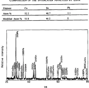
COMWSWION OF THE INTERLAYER ANALYZED BY EDX
Element c u Sn Pb
Atom YO 52 2 46 7 1 1
Modified Atom YO 53 8 46 2 0
Fig. 3. Cross-sectional view of electroless Cu on AIN substrate.
solutions as well as the plating conditions are summarized in Table I.
The electroless copper-plated specimens were cleaned in deionized water in an ultrasonic cleaner for 10 min, and then dipped into the M A - t y p e (4381 MA-type, multicore, Herfordshire, England) flux. The solder was a 63Sd37Pb eutectic alloy (SN63 eutectic, Multicore, Hertfordshire, Eng- land), and the solder bath was hold at 230°C. The substrate was vertically dipped into the bath for five seconds. The soldered specimen was then cleaned with a cleaning agent (PC81 cleaner, Multicore, Hertfordshire, England) in an ultrasonic cleaner for 20 min. The as-plated and/or soldered samples were then stored at 150°C for various times before investigation.
28
Fig. 6. The X-ray diffraction pattern of the soldered sample after 150-h
thermal storage at 15OOC.
The phase and crystal structure were identified with X-ray diffractometer (DMAX-B, Rigaku, Japan) with a wavelength of Cu Kcu (1.5406 A). The surface morphology and cross sec- tion view morphology were analyzed with a scanning electron
CHIOU er al.: METALLURGICAL REACTIONS AT THE INTERFACE OF Sn/Pb SOLDER AND ELECTROLESS COPPER-PLATED AlN SUBSTRATE 539
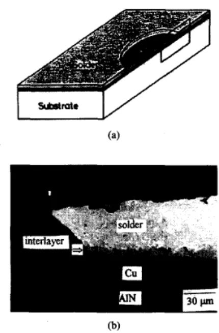
Fig. 7. Cross-sectional view of the soldered sample after 25 h storage at 15OOC. (a) SEM micrograph. (b) Cu X-ray mapping. (c) Sn X-ray mapping. (d) Pb X-ray mapping.
microscope (SEM) (250 MK3, Cambridge, UK) equipped with
EDX (Excel, Link, England).
The adhesion strength of Cu deposited on the AlN substrate is evaluated with a direct pull tester (SEBASTIAN FIVE, QUAD Group, USA). A stud was bonded perpendicularly to the coating surface with epoxy by holding it in contact through a spring mounting chip designed especially for the stud. The assembly was cured at 150°C for one hour. The stud was inserted into the platen and gripped. The tester pulled the stud and samples down against the platen support ridge until the coating or epoxy failed. The schematic diagram of the pull-off test is represented in Fig. 1. The force was increased slowly until failure occurred at F (kg). For the area, A (cm2) of the circular section of the stud, the pull strength, aa(kg/cm2), is defined as ua = F / A .
In.
RESULTS AND DISCUSSIONFig. 2 shows the surface morphology of the A1N substrate before plating. The micro-etching holes, as seen in Fig. 2, provide mechanical interlocking sites for the bonding of elec- troless copper to the A N substrate. The cross-sectional view of electroless Cu on AlN substrate is given in Fig. 3. It is observed that the electroless Cu tends to smooth the surface morphology of the substrate. This suggests that electroless copper plating is a potential approach for conformal via hole coating.
Thermal aging was employed to evaluate the Cu metalliza- tion. Fig. 4 exhibits the adhesion strength of electroless-plated Cu to A1N substrate after various times at 150°C. The adhe- sion strength after thermal storage for various time increases
% VI C 4, C 4, 0 # .- e CU .-
.-
eI
0 2 4 6 8 1 C Energy, keV (b) Fig. 8. (b) X-ray spectrnm.EDX analysis for the interlayer. (a) S E M cross-sectional view and
initially and then slightly decreases, as shown in Fig. 4. The mechanical properties of the electroless copper would affect the adhesion strength between electroless Cu and substrate. The temperature used for thermal storage test, 150°C is the recrystallization temperature of copper [27]. As is well known, a metal undergoing recrystallization experiences a great deal of ductility increase as well as a decrease in strength. Okinaka and Nakahara [28] argued that hydrogen is trapped in bubbles during deposition of electroless copper. They correlated the ductility of the electroless copper film with the cavity density and hydrogen baked out during annealing at 150°C. Pedraza and Godbole [27] reported that recrystallization of electroless copper resulted in a ten fold-increase in ductility and 40% decrease in tensile strength. Thermal aging the electroless copper plated substrate at 150°C results in recrystallization of electroless copper, and the ductility of the electroless copper is increased. It is rather difficult to form cracks at the electroless copper on the top of interlocking as the ductility of electroless copper prevails. Since the ductility of electroless copper tends to blunt crack propagation introduced during the pull-off test, the observed adhesion strength is then increased. The increase of strength during thermal storage is not appreciable, as indicated in Fig. 4. The adhesion strength, however, decreases slightly after 150°C storage because the elevated temperature (150°C) may cause deterioration on the electroless copper. Creep in the copper itself might be one of the possibilities. The adhesion strength of soldered samples as a function of storage time at 150°C is given in Fig. 5. There is a drastic drop in the adhesion strength after 25 h aging, where the
r ul
I I I I . I 1 i I I
20
30
40
50
60
70
IFig. 9. X-ray diffraction pattem of the fracture surface of soldered sample (a) top fracture surface and (b) bottom fracture Sample aged at 15OOC for 25 h.
adhesion is lower than 50 kg/cm2. Jones and Geckle reported the formation of intermetallic CusSn5 and Cu3Sn between the solder and the plated Cu on A1203 during high temperature storage [25], [26]. The X-ray diffraction pattern of soldered samples after 150 h thermal storage is shown in Fig. 6 , in which the Cu6Sn5 intermetallic compound is identified. The cross-sectional SEM micrographs and X-ray mapping of the soldered specimen after aging at 15OOC for 25 h is given in Fig. 7. The SEM micrograph in Fig. 7(a) clearly indicates that a distinct layer is formed between the solder and the electroless Cu. The X-ray mappings of Sn and Pb, shown in
Fig. 7(c) and 7(d) respectively, reveal that segregation of both Sn-rich and Pb-rich phases occur after the sample is aged for 25 h. Fig. 8 shows a magnified view of the interlayer and the X-ray spectrum for the interlayer analyzed by EDX. The quantitative analyses of the interlayer is listed in Table II. It should be pointed out that the electron probe size in the EDX analysis in the order of several microns appears to be larger than the interlayer width as shown in Fig. 8(a). As a consequence, the neighboring solder is also scanned even through the electron beam is located within the interlayer. This explains the measured 1.1 at.% Pb in the EDX analysis
CHIOU et al.: METALLURGICAL REACTIONS AT THE INTERFACE OF SdPb SOLDER AND ELECTROLESS COPPER-PLATED A N SUBSTRATE 54 1
1
I/
(b)
Fig. 10. Cross-sectional view of the fracture surface for the soldered sample after thermal storage at 15OOC for 25 h (a) schematic diagram and (b) SEM micrograph.
as indicated in Table 11. After extracting the undesired Pb and Sn due to the presence of Pb/Sn solder contents in the EDX quantitative results, one can normalize the measured Cu and remaining Sn and obtain a Cu/Sn ratio to be about
6 5 . The derived CusSn:, compound is in agreement with the
X-ray diffraction pattern as indicated in Fig. 6. Because the crack propagates through the intermetallic/Cu interface, the major concern is the adhesion between solder and electroless copper, not between the electroless Cu and the substrate. The intermetallic compound Cu&5 formed between the electroless copper and the solder would introduce stress in the interface which causes the crack to propagate. The X-ray diffraction pattern of the fracture surface is shown in Fig. 9. Intermetallics of Cu~Sn5 and Cu3Sn are found on the top of the fracture surface, while only Cu and a small amount of Cu3Sn are identified on the bottom of the fracture surface. The top fracture surface is the one attached to the stud after fracture, while the bottom fracture surface is the one associated with the underlying substrate. This implies that the crack propagates along the CusSn:,, Cu interface. The cross section view of the fracture surface is represented in Fig. 10, which confirms the fact that the crack propagates along the Cuhntermetallic interface. The adhesion strength before thermal storage is above 200 kg/cm2, while it decreases to below 50 kg/cm2 after 25 h thermal storage. Thus, it is argued that the presence of the intermetallic compound results in the decrease in adhesion strength, as indicated in Fig. 5.
The formation and growth of intermetallics at the sol- dedsubstrate interface are factors affecting the solderability and reliability of solder joints. Research on intermetallic growth in Cu-solder joints has concentrated on growth into relatively thick solder layers. Sunwoo et al. studied the growth of Cu-Sn intermetallics at a pretinned copper-solder interface
and observed the CusSn:, phase formation when Cu was wetted with eutectic solder at temperature below 400°C [29]. A recent study by Wu et al. revealed the diffusion behavior and microstructural evolution of Cu-Sn intermetallics at the composite solder/copper substrate interface [30]. The Cu-
containing composite solder generally formed CusSn5 layer. It was reported that Cu3Sn was never observed in any unaged sample using SEM due to the resolution limit, while it was only visible between the solder matrix and the copper substrate. This observation is similar to the one in this study in which no apparent Cu3Sn is found in the bulk soldered sample after 150 h thermal storage at 150°C as shown in Fig. 6. However, a small amount of CusSn is barely detected only on the fracture surface of the soldered sample, as indicated in Fig. 9. For inter- metallic formation and growth in the solder/substrate system, there exist diffusion through the growing intermetallic layer as well as an interfacial reaction. A more detailed investigation concerning the possible diffusion-controlled and/or interfacial reaction-controlled mechanism in the intermetallics formation between Sn/Pb solder and electroless Cu-plated A N substrate
will be reported in the near future.
IV. CONCLUSION
Intermetallic formation between electroless-plated cop- per and Sn/Pb solder is evaluated. The electroless-plated copper tends to smooth the surface morphology of the
AlN
substrate. This makes electroless Cu plating a promising approach for conformal via hole coating. The adhesion strength of Cu on AlN increases initially and then decreases after 150°C thermal storage. The increase in adhesion is attributed to the recrystallization of Cu at 150°C the ductile Cu tends to blunt crack propagation introduced during the pull-off test. The lower adhesion strength for longer aging time is caused by deterioration of Cu, such as creep, at 150°C. The adhesion strength of soldered samples decreases after 25 h at 150°C. Microstructural analysis of the soldered Cu/AlN assembly reveals the existence of an interlayer between solder and copper, and the segrega- tion of Pb-rich and Sn-rich phases. X-ray diffraction and EDX analysis results indicate the formation of intermetallic Cu&s at the interlayer.The intermetallic compound introduces stress concentra- tions in the interface which cause the crack to propagate along the intermetallic/Cu interface and results in the decrease in adhesion strength.
REFERENCES
[l] L. M. Sheppard, “Aluminum nitride: A versatile but challenging mate- rial,” Ceram. Bull., vol. 69, no. 11, pp. 1881-1891, 1990.
[2] R. R. Tummala, “Ceramics in microelectronic packaging,” in Advances in Ceramics, vol. 26, M. F. Yan, K. Niwa, H. M. OBryan, Jr., and W. S. Young, Eds. Westreville, O H American Ceramic Soc. Inc., 1989. [3] D. D. Marant and T. E. Nemecek, “Aluminum nitride: Preparation,
processing, and properties,” in Advances in Ceramics, vol. 26, M. F. Yan, K. Niwa, H. M. O’Bryan, Jr., and W. S. Young, Eds. Westreville, O H American Ceramic Soc. Inc., 1989.
[4] Y. Kurokawa, K. Utsumi, H. Takamizwa, T. Kamata, and S. Noguchi,
“AlN substrate with high thermal conductivity,” ZEEE Trans. Comp., Hybrids, Manufact. Technol., vol. CHMT-8, no. 2, pp. 247-252, 1985.
EEE TRANSACTIONS ON COMPONENTS, PACKAGING, AND MANUFACTURING TECHNOLOGY-PART B, VOL. 18, NO. 3, AUGUST 1995
A. J. Blodgett, “A multilayer ceramic multichip module,” IEEE Trans.
Comp., Hybrids, Manufact. Technol., vol. CHMT-3, pp. 624429, 1980. J. Wynschenk, “Electroless copper plating: Chemistry and maintenance,” Plating Surface Finishing, vol. 70, no. 1, pp. 28-29, 1983. P&SF Report, “Developments in electroless plating,” Plating Surface Finishing, vol. 71, no. 2, pp. 136-39, 1984.
J. Henry, “Electroless plating: Part III--Copper,” Metal Finishing, vol. 82, no. 11, pp. 47-48, 1984.
A. Hung, “Kinetic of electroless copper deposition with hypophosphite as a reducing agent,” Plating Surface Finishing, vol. 75, no. 4, pp. 74-77, 1988.
E. B. Saubestre, “Stablizing elecytroless copper solutions,” Plating, vol. 59, no. 6, pp. 563-566, 1972.
A. Molenaar, M. F. E. Hddrinet, and L. K. H. Van Beek, “Kinetics of electroless copper plating with EDTA as the complexing agent for cupric ions,” Plating, vol. 61, no. 3, pp. 23842, 1974.
F. J. Muzzi, “Accelerating the rate of electroless copper plating,” Plating Surface Finishing, vol. 70, no. 1, pp. 51-54, 1983.
J. Duffy, L. Pearson, and M. Paunvic, ‘The effect of pH on electronless copper deposition,” J. Electrochem. Soc., vol. 130, no. 4, pp. 876-880, 1983.
A. Hung, “Effect of thiourea and guanidine hydrochloride on electroless copper plating,” J. Electrochem. Soc., vol. 123, no. 5, pp. 1047-1049,
1976.
M. Pounovic and R. Amdt, “The effect of some additives on electroless copper deposition,” J. Electrochem. Soc., vol. 130, no. 4, pp. 794-799,
1983.
E. K. Yung and L. T. Romamankiw, “Plating of copper into through- holes and vias,” J. Electrochem. Soc., vol. 136, no. 1, pp. 206-215, 1989.
B. S. Chiou, G. H. Chang, and J. G. Duh, “Metallization of AIN substrates by electroless Cu plating,” Printing Surface Finishing, vol.
80. -., nu. rr 65-68. _ - --, 1993.
[IS] J. H. Chang, J. G. Duh, and B. S. Chiou, “Morphology and adhesion strength in electroless Cu metallized AIN substrate,” ZEEE Trans. Comp., Hybrids, Manufact. Technol., to be published.
[19] B. S. Chiou, K. C. Liu, J. G. Duh, and P. S. Palanisamy, “Intermetallic formation on the fracture of SniPb solder and PdAg conductor inter- faces,” IEEE Trans. Comp., Hybrids, Manufact. Technol., vol. 13, no. 2,
[20] -, “Temperature cycling effects between SniPb solder and thick film Pd/Ag conductor metallization,” IEEE Trans. Comp., Hybrids, Manufact. Technol., vol. 14, no. 1, pp. 233-237, 1991.
[21] G. D. O’clock Jr., M. S. Peters, J. R. Patter, G. A. Kleese, and R. V. Martini, “Pb-Sn microstructure: Potential reliability indicator for interconnects,” IEEE Trans. Comp., Hybrids, Manufact. TechnoI., vol. CHMT-10, no. 1, pp. 82-88, 1987.
[22] P. W. Dehaven, “The reaction kinetics of liquid 60/40 SdPb solder with copper and nickel: A high temperature X-ray diffraction study,” in Mat. Res. Soc. Symp. Proc., 1985, pp. 123-128.
[23] D. S. Dunn, T. F. Marinis, W. M, Sherry, and C. J. Williams, “De- pendence of CdSn and Cd6OSn4OPb solder joint strength on diffusion controlled growth of Cu3Sn and CU6Sn5,” in Mat. Soc. Symp. Proc., [24] C. W. Allen, M. R. Fulcher, A. S. Rai, G. A. Sargent, and A. E. Miller, “A study of intermetallic compound development in nikel-tin interfacial zones,” in Mat. Res. Soc. Sympl Proc., 1985, vol. 40, pp. 139-144. [25] W. K. Jones, “Evalutation of copper plated ceramic substrates,” in Proc.
Int. Symp. Hybrid Microelectronics, 1988, pp. 164-168.
[26] R. J. Geckle, “Metallurgical changes in tin-lead platings due to heat aging,” IEEE Trans. Comp., Pkg., Manufact. Technol., vol. 14, no. 4, pp. 691497, 1991.
pp. 267-274, 1990.
1985, pp. 129-138.
[27] A. J. Pedraza and M. J. Godbole, “Recrystallization and mechanical properties of electroless copper. 1,” Scripta Metall. Material., vol. 24, no. 7, pp. 1185-1189, 1990.
[28] Y. Okinaka and H. K. Straschil, ‘The effect of inclusions on the ductility of electroless copper deposits,’’ J. Electrochem. Soc., vol. 133, no. 12, [29] A. J. Sunwoo, J. W. Morris, Jr., and G. K. Lucey, Jr., “The growth of C u S n intermetallics at a pretinned copper-solder interface,” Metall. Trans., vol. 23A, pp. 1323-1332, 1992.
[30] Y. Wu, J. A. Sees, C. P. Povraghabagher, L. A. Foster, J. L. Marshall, E. G. Jocobs, and R. F. Pinizzotto, “The formation and growth of intermetallics in composite solder,” J. Electron. Mater., vol. 22, no. pp. 2608-2615, 1986.
7, pp. 769-777, 1993.
Bi-Shiou Chiou received the B.S. degree in nuclear engineering and the M.S. degree in health physics from the National Tsing Hua University (NTHU), Taiwan, and the Ph.D. degree in materials engineer- ing from Purdue University.
She is a professor at the Institute of Electronics, National Chiao Tung University, Hsinchu, Taiwan. She has been a visiting professor at Purdue Univer- sity and a visiting scientist at Comell. Her techni- cal interests include electronic ceramics, thick-film technology, thin-film deposition, and metallization in electronics packaging.
Jim-Haur Chang received the B.S. degree in ma- terials science from Feng-Chia University, Taiwan. He is a graduate student in the Department of Materials Science and Engineering, NTHU, Taiwan. His work involves metallization of aluminum nitnde substrate via electroless plating.
Jenq-Gong Duh received the B.S. degree in nuclear engineering from NTHU and the Ph.D. degree in matenals engineering from Purdue University.
He is a professor in the Department of Ma- terials Science and Engineering, NTHU, Tiuwan. From 1987 to 1988 he was a visiting scientist at Comell University and received the Best Teacher Award from NTHU. His technical interests include electron microscopy, interfacial phenomena of ma- terials, ceramic-metal bonding, and surface modifi- cation of ceramics.