國立交通大學
電信工程學系
碩士論文
雙頻帶圓極化天線及
雙頻帶高隔離度多重輸入多重輸出天線設計
Design of the Dual-Band Circularly Polarized Antenna and a Dual-Band High Isolation Multi Input Multi Output (MIMO) Antenna研究生:林易懋
指導教授:周復芳 博士
國立交通大學
電信工程學系
碩士論文
雙頻帶圓極化天線及
雙頻帶高隔離度多重輸入多重輸出天線設計
Design of the Dual-Band Circularly Polarized Antenna and a Dual-Band High Isolation Multi Input Multi Output (MIMO) Antenna研究生:林易懋
指導教授:周復芳 博士
雙頻帶圓極化天線及
雙頻帶高隔離度多重輸入多重輸出天線設計
Design of the Dual-Band Circularly Polarized Antenna and a Dual-Band High Isolation Multi Input Multi Output (MIMO) Antenna研究生:林易懋 Student:Yi - Mao Lin 指導教授:周復芳 博士 Advisor: Dr. Christina F. Jou
國立交通大學 電信工程學系碩士班
碩士論文
A Thesis
Submitted to Department of Communication Engineering College of Electrical and Computer Enginerring
National Chiao Tung University In Partial Fulfillment of Requirements
For the Degree of Master of Science
In Communication Engineering
June 2012
Hsinchu, Taiwan, Republic of China
雙頻帶圓極化天線及
雙頻帶高隔離度多重輸入多重輸出天線設計
研究生:林易懋 指導教授:周復芳 博士 國立交通大學電信工程學系碩士班 中文摘要 本篇論文提出兩種類型天線之設計。一是雙頻帶圓極化天線之研究,另一主 題是探討高隔離度之多輸入多輸出天線 首先,針對第一個主題,由螺旋型圓極化天線做為理念,我們將以簡易的圓 型分支路徑,使電流流向為圓形,產生圓極化之效果之天線。以不同分支使共振 頻帶達到雙頻,再藉由主要路徑電流流向產生圓極化。除此之外,面臨正 Z 軸 左手圓極化增益較小之問題,我們在背後基版增加一圓形貼片,將此圓型貼片當 作反射鏡面使用。將邊緣波束整體往上反射。由模擬及實驗結果證明,此貼面確 實可增加一部分之增益。 另一個主題,在此我們討論一種增加天線之間隔離度之方法,一般多輸入多 輸出之天線,天線之間存在著很高的耦合量,對於訊號之傳輸有著干擾,為避免 此問題,文獻[1]設計是在天線之間增加一電感性分支,亦或是增加一電感性元 件,在文獻[2]提出,在接地面上設計一槽空,使其達到提高隔離度之效果。我 們將參考之前論述,簡易的在接地面適當位置做出幾個凹槽,此凹槽可等效為電 容電感元件串聯,當在適當頻率共振時,可視作此凹槽在輻射一部分能量,阻隔 兩天線之間輻射之干擾。 此兩支天線皆設計在 2.5GHz 及 5.2GHz,以供無線區域網路頻段之應用。Design of the Dual-Band Circularly Polarized Antenna and a Dual-Band High Isolation Multi Input Multi Output (MIMO) Antenna
Student: Yi Mao Lin Advisor: Dr. Christina F. Jou
Department of Communication Engineering College of Electrical and Computer Engineering
National Chiao Tung University
Abstract
This paper proposes two designs of antennas. One is the research of the dual band circularly polarized antenna and another design is dual band high isolation multi input multi output (MIMO) antenna.
For the first topic, according the spiral antenna, we designed the circularly polarized antenna with circular strips. It made the current go to circular paths. To improve the Left Hand Circularly Polarization (LHCP) gain at positive z axial. We added a circular pad on the back of the substrate. From the simulation and measurement, it observed that the LHCP gain enhanced, really.
Then, another topic, we discussed the method to enhance the isolation between two port antennas. According some reference, high isolation was achieved by etching slits into the ground plane[2]. Ground branches were applied in to achieved low mutual coupling within a narrow frequency band. Parasitic elements were added to improve the port isolation of a MIMO antenna[1]. In this work, we studied the slot line on the ground, the slot line could equivalent to RLC series circuit, when it at
The two proposed antennas are designed at 2.5GHz and 5.2GHz, they could be applied on wireless communication.
誌謝
能夠順利完成這篇碩論,以及取得這碩士學位,首先感謝周復芳教授,謝謝 您的指導,讓我對天線領域有了收穫,您的包容,讓我能隨心所欲的發揮創意做 研究,進而在研究上有了成果。感謝口試委員王健仁老師以及吳俊緯學長,你們 在碩論上細心的指正以及建議,使的這篇碩論更加的完善。謝謝學長沈爽(宜星)、智鵬,因為你們,讓我知道如何玩的快樂,同時也把 研究顧好,有效率的把事情做好。謝謝沈爽,忘不了我們第一次所討論的研究, 以及 2 年來你三不五時抽查我的進度。將來有機會,再來切磋。 謝謝學長舜哥(超舜),謝謝你在我碩二心背離電波組時仍然沒有放棄我,及 時的抓住我,也謝謝一路來對我的研究給了那麼多的建議。 感謝已畢業的學長姐們: 謝謝仁哥(蘇阿姨),謝謝妳讓我在碩一時有那麼多梗,也讓我為大家帶來那 麼多的歡樂。 謝謝李哥(政廷),謝謝你從一開始教我怎麼用軟體設計 Monopole,到一起 去逛大潤發、後火、竹北『大』夜市、大廚,到你畢業之後都還一直關心我的研 究、研替。 謝謝卡爺(政皓),雖然整天聽你在ㄜㄜ叫,感謝那時對於 Sinuous 的幫忙, 你讓我學到如何對一件事情專注、執著。以及什麼叫做 HFSS『自己摸摸就會』。 謝謝林學友(子淵),你是我天線研究上的 3 位師父之一,每次的出遊也一定 都有你,更感謝你在我尾牙以及 SNSD 二巡去台北時的招待。鼎王、唱歌、桌遊 都成為我們共同的回憶。 謝謝胖股-股小燕(珮玲),謝謝妳在我一開始單槍匹馬尬數位通訊時幫我拿 到的資源,更忘不了在數位通訊期中考的前一天,我們那一群在交映樓下喝酒喝 通霄的時光。也還記得我們鼎王逢甲行回來還續攤到湯姆熊的瘋狂。 謝謝阿九(伯儒),永遠記得進來實驗室的第一個月大家去你家過中秋節烤肉,
你這學長真的是沒話說的讚,還記得你碩 2 我們天天互嗆完 Battle 的場景,是 你教我什麼叫做『爽派的認真』,謝謝你和胖股,沒有你們 2 位,我就不會在 919, 我真的是因為你們 2 位才進來 919 的。 再來是同窗: 謝謝阿牟(家宏),碩一下沒有你和你麻吉的援助,我就無法生出那玩具去澳 洲玩。 謝謝建榮,要不是你,真不知我會拖到什麼時候才會想去口試,感謝你在最 後那一段時間的幫忙,讓我得以順利的完成碩班一途的最後一關。回想起在量天 線那時,其實跟你論道還蠻好玩的啦!哪天等我進修變強一點再開論壇好了。 謝謝小賴(星翰),謝謝你碩一時和子淵一同把我引進 SNSD 的世界,讓我知 道,有信念,真的就不怕困難能做好事情。更感謝你不辭辛苦的規畫行程帶我們 去澳洲玩,那幾天也成為我永生難忘的回憶。 以及我最羨慕的學弟妹們: 謝謝助教(寶國),回想起一起修微波工程(一)時的情形,除了執著、認真、 以及跳針...阿不是。從你身上,我亦學到了許多就是。 謝謝馮盛,從第一次的『打印機』,中間的『短信』,到最後與一代神人『史 密斯』的交會,謝謝你,幫我拍的那幾張照片,我真的好喜歡。 謝謝胖妹(涵婷),妳和某翔的一搭一唱,為這實驗室帶來了許多歡樂。妳不 胖啦,我常叫八叫錯叫成胖而已。 謝謝大師(佑祥),你那憨厚真誠的笑容,讓我知道人生其實可以更快樂,每 次你都說我講話很好笑,其實帶給我歡樂的人是你,還記得火鍋快結束時你那怦 然心動的會心一笑,不用懷疑,衝~ 謝謝阿翔(雨翔),最先感謝你 AIC 的幫忙,以及策劃南寮,六福村,雖然我 知道...,不過那 2 次,也成為我人生難忘的一頁。 謝謝阿倫(玠倫),謝謝你在微波、高磁不惜出賣自己靈魂替我拿到的資源, 沒有你的幫忙,我還真不知我能不能畢業呢。我能教你這直屬學弟的都教你啦,
之後就看你自己造化啦,切記,誰都可以學,就是不要學數理易懋背離他自己的 研究。 謝謝秀大軍師-阿秀(瑜秀),最先感謝妳一進來就把我麻吉搶過去,以後她 就勞煩妳多照顧了嘿!也謝謝妳陪我去韓格舖當我的軍師,在韓格舖的一席話, 讓我知道接下來我該如何做選擇。 特別感謝: 謝謝帶我的學長搭撥(玠瑝),謝謝你,在我碩一下時研究當我的後盾,讓我 知道我該怎麼處理。除了研究上的幫忙以及指導之外,你是教我如何幫助人當中 的其中一位,謝謝你,在我一人荒唐的在 11 舍 7-11 熬夜排哀蹦搶 SNSD 二巡票 時那消夜和中餐的探望與相陪,也謝謝你在我車禍時完全不問理由不吭一聲的陪 伴相挺。 碩班 2 年生活能有各位的幫忙,是易懋之幸。有你(妳)們,讓我順利完成碩 班的學業以及這篇論文,謝謝你(妳)們! 謝謝我的家人,爸爸、媽媽、姊姊對我的包容,在我背離我的心時仍然對我 給予鼓勵沒有放棄我,爸爸你一生投資無數,最失敗的投資應該就是投資在我身 上吧,但你放心,往後的人生我會再站起,不會辜負你的期待。謝謝媽媽對我的 疼愛,當我在抱怨以及背離時,傾聽我的訴說與給予我的建議。謝謝姊姊適時提 醒我瘋狂追星的行為,以及對我生活上的督促與幫忙。 最後,謝謝妳,雖然當初這 2 支『天線的形狀』都不是為妳而排,但最後完 成的喜悅,卻是最先也最想和妳分享,謝謝妳,讓我找回初心,不再怨悔,謝謝 妳,給過我今生最快樂卻也是過的最快的一個月時光。能遇上妳,是我碩班 2 年最後的幸福。對不起,謝謝妳...千言萬語道不盡,掌動天地伏龍鳴。 最後再說一次~現在是 919,以後是 919,永遠是~919 林易懋 於 酆都交大 2012.06
Table of the Contents
中文摘要...I Abstract...II 誌謝...IV TABLE OF CONTENTS...VII LIST OF FIGURES...IX LIST OF TABLES ...XIICHAPTER 1 ... 1
INTRODUCTION ... 1
1.1MOTIVATION... 1
1.1.1Motivation of Circular Polarized Antenna ... 1
1.1.2Motivation of Dual Band MIMO Antenna... 2
1.2ORGANIZATION ... 3
CHAPTER 2 ... 4
A 2.5/5.2GHZ DUAL-BAND CIRCULARLY-POLARIZED ANTENNA ... 4
2.1 BASIC THEORY ... 4
2.1.1 Theory of the Microstrip Line Structure ... 4
2.1.2 Formulas for Effective Dielectric Constant, Characteristic Impedance, and Attenuation ... 7
2.1.3 Polarization ... 9
2.2 2.5/5.2GHZ DUAL-BAND CIRCULARLY-POLARIZED ANTENNA DESIGN ... 14
2.2.1 Schema of Antenna Structure ... 15
CHAPTER 3 ... 29
A 2.5/5.2GHZ DUAL BAND MIMO ANTENNA ... 29
3.1 BASIC THEORY ... 29
3.1.1 Theory of Multiple-Input Multiple-Output (MIMO) Antenna... 29
3.1.2 Theory of Half-Wave Dipole Antenna ... 31
3.1.3 Theory of the Image Theory ... 34
3.1.4 Theory of the Monopole ... 36
3.1.5 Theory of the Defected Ground Structure ... 37
3.1.6 Modeling of Defected Ground Structure (DGS) ... 38
3.1.7 LC and RLC Equivalent Circuit Modeling ... 38
3.2 2.5/5.2GHZ DUAL BAND MIMOANTENNA DESIGN ... 42
3.2.1 Design 2.5/5.2GHz Dual Band SISO Antenna ... 42
3.2.2 Design 2.5/5.2GHz Dual Band MIMO Antenna ... 43
3.2.2 Using DGS Structure to enhance the Isolation between Two Antenna elements ... 46
3.3 SIMULATION AND MEASUREMENT RESULTS FOR 2.5/5.2GHZ DUAL BAND MIMOANTENNA ... 51
3.4 CONCLUSION ... 59
CHAPTER 4 ... 60
CONCLUSION AND FUTURE STUDY ... 60
4.1 CONCLUSION AND SUMMARY ... 60
4.2 FUTURE STUDY ... 61
LIST
OF
FIGURES
Fig. 2.1 Geometry of microstrip line ... 6
Fig. 2.2 Electric and magnetic field lines of microstrip line ... 6
Fig. 2.3 RHEP with traveling direction in the +z-axis and tilt angle τ with respect to the principle axis ... 12
Fig. 2.4 Modified-axis RHEP presentation ... 13
Fig. 2.5 Geometry of the proposed antenna (a) Top side view (b) Back side view .. 16
Fig. 2.6 Main structure of the proposed antenna (a) Top side view (b) Back side view ... 18
Fig. 2.7 Return loss of the main structure antenna ... 18
Fig. 2.8 The simulated axial ratio of the main structure antenna ... 19
Fig. 2.9 Surface current distribution for the main structure antenna ... 19
Fig. 2.10 The main structure antenna with the slot on the ground (a) Top side view (b) Back side view ... 20
Fig. 2.11 Surface current distribution for the proposed antenna at 5.2GHz ... 21
Fig. 2.12 The variation of the 5.2GHz axial ratio with the D1 ... 21
Fig. 2.13 Geometry of the proposed antenna (a) Top side view (b) Back side view ... 22
Fig. 2.14 LHCP gain at positive z-direction with different R2 ... 23
Fig. 2.15 The measured and simulated results for Return Loss curve of the proposed antenna ... 24
Fig. 2.16 The measurement and simulated results for axial ratio curve of the proposed antenna ... 25
Fig. 2.17 Measurement LHCP and RHCP radiation patterns of the proposed antenna at YZ plane (a) 2.5GHz (b) 5.2GHz. ... 26 Fig. 2.18 Simulated and measurement LHCP radiation patterns of the proposed
antenna at YZ plane (a) 2.5GHz (b) 5.2GHz ... 27
Fig. 2.19 The comparison with circular pad on the back of the substrate and LHCP gain at positive z direction. ... 27
Fig. 2.20 Fabricated the proposed antenna (a) front view (b) back view ... 28
Fig. 3.1 The diagram of SISO, SIMO, MISO,MIMO... 32
Fig. 3.2 The half-wave dipole (a) Current distribution I(z) and (b) Far-field radiation pattern F(θ) ... 33
Fig. 3.3 Ideal dipole above and perpendicular to a perfectly conducting ground plane Physical model and (b) Equivalent model using image theory ... 35
Fig. 3.4 Ideal dipole above and parallel to a perfectly ground plane Physical model and (b) Equivalent model using image theory ... 36
Fig. 3.5 Ideal dipole above and obliquely oriented relative to a perfectly ground plane Physical model and (b) Equivalent model using image theory ... 36
Fig. 3.6 Monopole antenna over perfect ground plane with their image (dashed) ... 36
Fig. 3.7 Side view of Dumbbell-shaped DGS... 39
Fig. 3.8 Top view of Dumbbell-shaped DGS ... 39
Fig. 3.9 LC equivalent circuit of single cell dumbbell-shaped DGS ... 40
Fig. 3.10 One-pole Butterworth prototype Low Pass Filter... 40
Fig. 3.11 The main structure of antenna with one element (a) Top side view (b) Back side view ... 42
Fig. 3.12 Simulated return loss of one element antenna ... 43
Fig. 3.13 The main structure of the MIMO antenna (a) Top side view (b) Back side view ... 44
Fig. 3.14 Simulated return loss of main structure MIMO antennas ... 44
(b) Back side view ... 47
Fig. 3.17 The comparison isolation with and without the middle slit ... 47
Fig. 3.18 The comparison surface current distribution at 2.5GHz ... 48
Fig. 3.19 The proposed 2.5/5.2GHz dual band MIMO antenna structure (a) Top side view (b) Back side view ... 49
Fig. 3.20 The comparison of return loss with and without the two slits ... 50
Fig. 3.21 The comparison isolation with and without the three slots ... 50
Fig. 3.22 The simulated return loss of the proposed MIMO antenna ... 52
Fig. 3.23 The measurement return loss of the proposed MIMO antenna ... 52
Fig. 3.24 The measurement and simulated results for isolation of the proposed antenna ... 53
Fig. 3.25 The port 1 radiation pattern about simulated and measurement result at 2.5 GHz (a) XY plane (b) YZ plane (c) XZ plane ... 54
Fig. 3.26 The port 2 radiation pattern about simulated and measurement result at 2.5 GHz (a) XY plane (b) YZ plane (c) XZ plane ... 55
Fig. 3.27 The port 1 radiation pattern about simulated and measurement result at 5.2 GHz (a) XY plane (b) YZ plane (c) XZ plane ... 56
Fig. 3.28 The port 2 radiation pattern about simulated and measurement result at 5.2 GHz (a) XY plane (b) YZ plane (c) XZ plane ... 57
Fig. 3.29 Computed envelope correlation for the MIMO configuration ... 58
LIST
OF
TABLES
Table2.1 Dimension of the Proposed Antenna ……….16
Table3.1 Dimension of the Single element Antenna……….42
Table3.2 Dimension of The Main Structure of the MIMO Antenna ………....45
C
HAPTER
1
I
NTRODUCTION
1.1 Motivation
1.1.1Motivation of Circular Polarized Antenna
Circularly polarized (CP) antennas have attracted much attention for mobile wireless and satellite communications because they allows for greater flexibility in orientation angle between transmitter and receiver antennas, better mobility and weather penetration, and reduction in multipath reflections[3, 4]. Circularly polarized antennas have been especially employed in modern communication systems sensitive to atmospheric variation, such as radar tracking, navigation, satellite systems, radio frequency identification (RFID), sensor systems, and mobile communication systems.[5-7]
In general, the radiation patterns of printed antennas are linearly polarized (LP); they are difficult to radiate circularly polarized radiation wave generated by two near-degenerated orthogonal resonated modes of equal amplitude and 900 phase difference. Another to generate circularly polarized radiation wave method is let the current paths circular, such as spiral antennas[4, 8-10]. With spiral antenna, the feeding is a hard work. We applied the circular path idea, but we chose the microstrip feeding network. Microstrip antennas are attractive to present wireless communication products because of the features of low profile, low cost and easy manufacture.
The proposed antenna is compact with overall size on 50mm x 50mm printed on FR4 substrate. In this paper we present a novel structure antenna that can provide dual-band CP radiation for wireless application
1.1.2Motivation of Dual Band MIMO Antenna
Nowadays, there is a demand to increase the data rate of existing wireless communication systems. The application of diversity techniques, most commonly assuming two antennas in a mobile terminal, can enhance the data rate and reliability without sacrificing additional spectrum or transmitted power in rich scattering environments[11, 12]. When a MIMO antenna system is applied in a multifunctional portable device, wideband and high isolation are demanded. Various techniques have been reported to enhance isolation between the elements of a MIMO antenna system. High isolation was achieved by etching slits into the ground plane[13]. Ground branches were applied in [14] to achieved low mutual coupling within a narrow frequency band. Parasitic elements were added to improve the port isolation of a MIMO antenna system[15]. Since the implementation of additional parasitic elements occupies a significant space, this technique is not attractive for handset devices.
In practice, low-profile planar antennas are more preferred so that antenna radiators can be easily integrated with other printed circuit board (PCB) components in portable devices. The dual band MIMO antenna was fabricated on FR4, and the size was 65mm x 45mm. For the purpose, the MIMO antenna covers 2.4GHz
WLAN(2400-2480MHz), 2.5GHz WiMAX(2500-2690MHz), 5.2GHz
WLAN(5150-5350MHz), 5GHz WiMAX(5250-5850MHz) and 5.8GHz WLAN (5725-5825MHz).
1.2 Organization
Thus dissertation is divided to four chapters and is organized as follows: In chapter 1, the outline and the motivations of two researches are introduced. In chapter 2, we will present the dual band circularly polarized antenna with double C shape strips structure. Before that we will introduce some basic theories such as microstrip network, Linear polarization, Elliptical polarization, Circular polarization and Axial ratio. After introduced the antenna structure, we will show the simulation and the measurement of the proposed antenna and make a short conclusion.
Next, in chapter 3, we will demonstrate a dual band MIMO antenna system with the defected ground structure (DGS) on the ground. We also introduced basic theories such as half-wave dipole antenna, imaged theory, and monopole antenna. And we will show the performance after we introduced the structure of the MIMO antenna. Finally, in chapter 4, we will give the summary and the conclusion of all and future study.
C
HAPTER
2
A
2.5/5.2GH
Z
D
UAL
-B
AND
C
IRCULARLY
-
POLARIZED
A
NTENNA
In this chapter, a 2.5 / 5.2GHz dual-band Circularly-polarized Antenna antenna is presented here. We design the feeding network by using the microstrip structure. Microstrip antennas are attractive to present wireless communication products because of the features of low profile, low cost and easy manufacture. For the dual-band design, there are two major current paths to radiate. To generate circular polarization, we use the C shape circular strip to radiate. At this work, the simulator is based 3-D full-wave EM solver, Ansoft HFSS. Here, we will display the simulation result of this design.
2.1 Basic Theory
2.1.1 Theory of the Microstrip Line Structure
Microstrip line[16] is one of the most popular types of planar transmission lines, because it can be fabricated by photolithographic processes and is easily integrated with other passive and active microwave devices. The geometry of a microstrip line is shown in Figure 2.1. A conductor of width W is printed on a thin, grounded dielectric substrate of thickness d and relative permittivity
ε
r.
A sketch of the field line is shown in Figure 2.2.If the dielectric constant is equal to the dielectric constant as a free space, we could think of the line as a two-wire line consisting of two flat strip conductors of width W, separated by a distance 2d (the ground plane can be removed via image
theory). In this case we would have a simple TEM transmission line, with vp=c and
β =k0.
The presence of the dielectric, and particularly the fact that the dielectric does not fill the air region above the strip (y>d), complicates the behavior and analysis of microstrip line. Under stripline, where all the fields are contained within a homogeneous dielectric region, microstrip has some (usually most) of its field lines in the dielectric region, concentrated between the strip conductor and ground plane, and some fraction in the air region above the substrate. For this reason the microstrip line cannot support a pure TEM wave, since the phase velocity of TEM fields in the dielectric region would be c
εr but the phase velocity of TEM fields in the air region
would be c. Thus, a phase match at the dielectric-air interface would be impossible to attain for a TEM-type wave.
In actually, the exact fields of a microstrip line constitute a hybrid TM-TE wave, and require more advanced analysis techniques than we are prepared to deal with here. In most practical applications, however , the dielectric substrate is electrically very thin (d<<λ ), and so the fields are quasi-TEM. In other words, the fields are essentially the same as those of the statics case. Thus, good approximations for the phase velocity, propagation constant and characteristic impedance can be obtained from static or quasi-static solutions. Then the phase velocity and propagation constant can be expressed as
v
p=
cϵe (2.1.1)
β = k
0ϵ
e (2.1.2)where ϵe, is the effective dielectric constant of the microstrip line. Since some of the field lines are in the dielectric region and some are in air, the effective dielectric constant satisfies the relation
1 < ϵ
e< ϵ
r (2.1.3) and is dependent on the substrate thickness, d, and conductor width W. We will first present design formulas for the effective dielectric constant and characteristic impedance of microstrip line; these results are curve-fit approximations to rigorous quasi-static solutions[17, 18]Fig. 2.1 Geometry of microstrip line [14]
2.1.2 Formulas for Effective Dielectric Constant, Characteristic Impedance, and Attenuation
The effective dielectric constant of a microstrip line is given approximately by
∈
e=
∈r+1 2+
∈r−1 2 1 1+12d w (2.1.4)The effective dielectric constant can be interpreted as the dielectric constant of a homogeneous medium that replaces the air and dielectric regions of the microstrip. The phase velocity and propagation constant are then given by Eq(2.1.1) and Eq(2.1.2). Given the dimensions of the microstrip line, the characteristic impedance can be calculated as
Z
0=
60 ∈eln
8d w+
w 4dfor
W d≤ 1
120π ϵe w d+ 1.393 + 0.667ln
w d+ 1.444 for
W d≥ 1
(2.1.5)
For a given characteristic impedance Z0 and dielectric constant ∈r, and W d ratio can be found as W d = 8eA e2A−2 for W d < 2 2 π B − 1 − ln 2B − 1 + ∈r−1 2 ln B − 1 + 0.39 − 0.61 ϵr for W d < 2 (2.1.6) where
A =
Z0 60 ϵr+1 2+
∈r−1 ∈r+10.23 +
0.11 ϵr(2.1.7)
B =
377π 2Z0 ∈r (2.1.8) Considering microstrip as a quasi-TEM line, the attenuation due to dielectric loss can be determined asα
d=
k0∈r(∈r−1)tan δ
where tanδ is the loss tangent of the dielectric, which account for the fact that the fields around the microstrip line are partly in air (lossless) and partly in the dielectric. The attenuation due to conductor loss is given approximately by [15]
α
c=
RsZ0W (2.1.10)
where Rs = ωμ0 2ς is the surface resistivity of the conductor. For most microstrip
substrates, conductor loss is much more significant than dielectric loss; exceptions may occur with some semiconductor substrates.
2.1.3 Polarization
According to the concept of displacement current, James C. Maxwell got agreement with other electromagnetic equations and predicted the existence of electromagnetic wave since more than a century ago. In the far-field region, energy radiation caused by current distribution on antennas can be seen as a transverse electromagnetic (TEM) wave - the components of electric field (E), magnetic field (H) and propagating direction are perpendicular each other none the loss because they vary with time. The term Polarization can only use the trajectory of time-varying E in space to identify behavior of microwave radiation due to the relation between E and H as (2.1.11).
Generally, infinitesimal current I with ∆z ≪ λ in length on the antenna can be seen as an equal length ideal dipole possesses both uniform magnitude and phase[19]. Such an ideal dipole illuminates in free space to form a doughnut-like radiation pattern without inner hollow and hence polar plots with omni-direction and figure-of-eight are revealed through the cross-section vertical and horizontal to the dipole separately. In a practical sense, H plane presents the vertical cutting mentioned above as it contains H vector and E-plane indicates the other for the same reason. The wave is referred as to a planer wave while observation point is stationed adequately far from radiating source, and its E vector and H vector are co-located on the constant phase plane. Selecting any constant phase plane as an observation plane with time-varying condition, a trajectory constructed by the tip of E vector can be obtained.
Eθ Hφ
=
ωμ β=
ωμ ω μϵ=
μ ε= η
(2.1.11)E
= E
θθ =
I∆z 4πjωμ
e−jβ r rsin θ θ
(2.1.12)H
= H
φφ
=
I∆z 4πjβ
e−jβ r rsin θ φ
(2.1.13) Linear PolarizationIt would be examined further the radiating properties of ideal dipole referred before. Once the dipole vertical to ground is placed in free space, the tip of time-varying E vector will go back and forth along a straight line perpendicular to ground and the wave is so-called vertical polarization. Horizontal polarization presents time-varying E vector which varies with the straight line parallel to ground by the same token. The situation a wave polarized in the x-direction is traveling along the +z-axis can be written as following:
E
= x E
xe
−jkz (2.1.14) To deserve to be mentioned, 45-degrees polarization is obtained as the included angle of 45 degrees between dipole and ground plane is illustrated. It would be obtained in the situation such as dual-polarized application. After the discussion of three kinds of the polarization type, it can be attached the triple to linear polarization because of the orbits caused by them are linearity.A coordinate system is further established on an observation plane to describe the behaviors of polarization through two orthogonal bases - Ev and EH, which means
that the electric field distribution in free space would be composed of Ev and EH even
through it varies with time. The classifications of polarization are completed according to combinations of the bases and hence circular polarization and elliptical polarization will be considered.
Elliptical Polarization
vectors. In other words, the tips of vectors on the observation plane depict an ellipse with respect to time varying. It would be judged which is a left polarization or right polarization according to phase relation between these two components. Take a simple example: it is a left polarized wave as observer faces the incoming wave and the vector combined by generating sets rotates clockwise. It can be considered the situation a wave of component leads y-component by +90 degrees is traveling along the z-axis forms the right hand elliptically polarized wave. It would be expressed as following:
E
= x E
xe
−jkz− y jE
ye
−jkz (2.1.15) The expression gives a good account of the fact that an elliptical polarized wave can be decomposed to a couple of linear polarized waves which are perpendicular each other in space as well as are 90 degrees out of phase. In physical sense, it presents this phenomenon obviously and hints elliptically polarization can be as a general solution to derive other polarized types. Generally speaking, elliptical polarization is a kind of conventional polarization type in everyday life.Circular Polarization and Axial Ratio
Circular polarization would be constructed as imposing a restriction of generating components with equal quantity on the elliptical polarization. As implied by the name, the vector remains constant in length and rotates around in a circular path. Similarly, the discrimination between left-hand circular polarization (LHCP) and right-hand circular polarization (RHCP) will be done through the rotational sense by vector as the wave travels toward the observer.
After the discussion, it would be derived to the question which one parameter could identify the types of polarization. It should be concentrated on the interpretation of axial ratio and the extended discussion of elliptical polarization will be considered.
Y
Fig. 2.3 RHEP with traveling direction in the +z-axis and tilt angle τ with respect to the principle axis
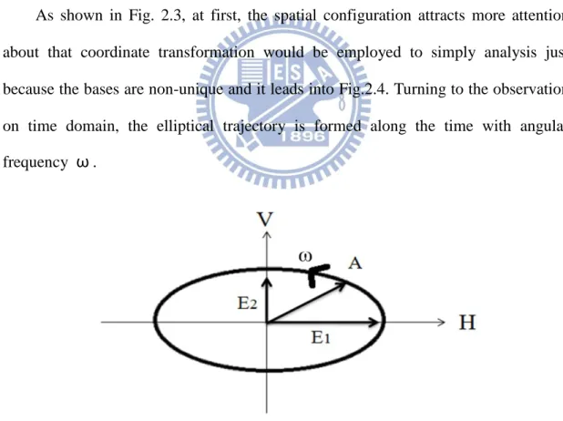
As shown in Fig. 2.3, at first, the spatial configuration attracts more attention about that coordinate transformation would be employed to simply analysis just because the bases are non-unique and it leads into Fig.2.4. Turning to the observation on time domain, the elliptical trajectory is formed along the time with angular frequency ω .
Fig. 2.4 Modified-axis RHEP presentation
The H-component equals to E1 and no V-component as point A lies on the H-axis,
V-axis. The H-component leads V-component by 90 degrees according to the pasting angle is about 90 degrees. Polarized behavior can be described in terms of space and time and axial ratio can be written as following:
AR = 20log Emax
Emin (2.1.16)
Where Emax means maximum value of E along major axis and Emin means maximum value of E along minor axis.
In conclusions,
(1) Linear polarization:(AR → ∞) Uni-axis or bi-axial with in phase (2) Elliptical Polarization:(AR ≥ 0dB)
Bi-axis with quadrature phase (3) Circular Polarization:(AR = 0dB)
Bi-axis with identical magnitude and quadrature phase
2.2 2.5/5.2GHz Dual-Band Circularly-polarized Antenna Design
In this chapter, a 2.5/5.2GHz dual-band circularly-polarized of a monopole antenna fed through microstrip line is proposed. The proposed antenna is achieved using microstrip-fed with two circular strips and two circular patches. One circular strip radiates lower band, the other one covers higher band. By adding the circular patch on the back of the substrate, the left-hand circular polarization (LHCP) gain at the positive z axial of this proposed antenna has been improved. The antenna operates in two bands which are 2.5GHz and 5.2GHz. These two operating bands can be applied for the WiMax and WLAN application. Fig.2.5 shows the configuration of our proposed dual band circularly polarized antenna. The antenna is fabricated on an FR4 substrate with a dielectric constant of 4.4 and a loss tangent of 0.02. The thickness of the substrate is 1.6 mm. The size of the antenna is ( G × G ) 50 mm × 50 mm which is suitable for most mobile devices. Experimental results show the proposed antenna has good return loss and circular polarization characteristics. The 10 dB return loss impedance bandwidths for the lower band (2.5GHz) and higher band (5.2GHz) are 50% and 23%, respectively. The 3dB axial-ratio bandwidths are 14.8%and 4.0% with respect to 2.5GHz and 5.2GHz, respectively.
2.2.1 Schema of Antenna Structure
The geometry of the proposed antenna was shown as Fig.2.5. It consists of two circular strips and two circular pads. The two circular strips length are L1 and L2
respectively, and the two circular patch radii are R1 and R2 respectively. One circular
patch which is placed on the upside of the substrate is used to improve the input impedance matching, the other patch is etched on the other side of the substrate is used to enhance the higher band LHCP gain at the positive z axial. The antenna is fabricated on an FR4 substrate with a dielectric constant of 4.4 and a loss tangent of 0.02. The thickness of the substrate is 1.6 mm. The size of the antenna is ( G × G ) 50 mm × 50 mm which is suitable for most mobile devices. The width of feeding line is w=3 mm for a 50 Ohm impedance. The outer and longer circular strip (L1) is about 70
mm, it radiates for lower band, the inner and shorter strip (L2) whose length is about
33 mm is operating for higher band. The adding slot of the ground plane is for lower band matching. The optimized parameters of the proposed antenna dimensions are listed in Table 2.1
Fig. 2.5 Geometry of the proposed antenna (a) Top side view (b) Back side view
Variable w L1 L2 R1 R2 F1 G R D1 D2
Value(mm) 3 70 33 7.5 10 18.5 50 10.8 5.3 3
2.2.2 The part of the structure discussion
A. The Main Structure of the Proposed Antenna
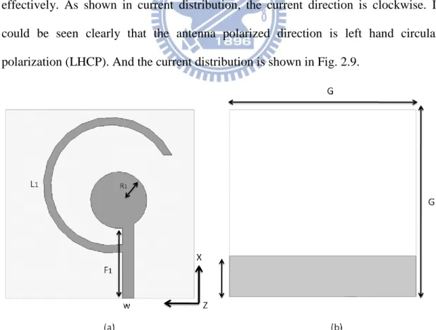
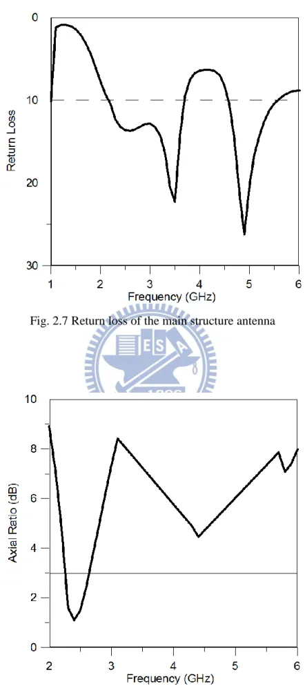
As shown in Fig.2.6. It is the main structure of the proposed antenna. To generated 2.5GHz band. First, it uses a C shape circular strip and a circular patch to generate the 2.5GHz band. And with the circular patch, it generates good impedance in 5.2GHz band. The return loss is plotted in Fig. 2.7. A typical technique for generating circular polarization radiation is to excite two orthogonal degenerate resonant modes with a 90o phase difference. In this work, we use a circular strip to exited 2.5GHz band and generated circular polarization radiation. Besides the circular strip, the asymmetric feeding is used. The simulated of axial ratio is shown in Fig. 2.8. Asymmetric feeding possess lower and almost steadfast axial ratio and hence it can be concluded asymmetric feeding technique improves circularly polarized performance effectively. As shown in current distribution, the current direction is clockwise. It could be seen clearly that the antenna polarized direction is left hand circular polarization (LHCP). And the current distribution is shown in Fig. 2.9.
Fig. 2.7 Return loss of the main structure antenna
Fig. 2.9 Surface current distribution for the main structure antenna
B. Generated the 5.2GHz Band Circular Polarization
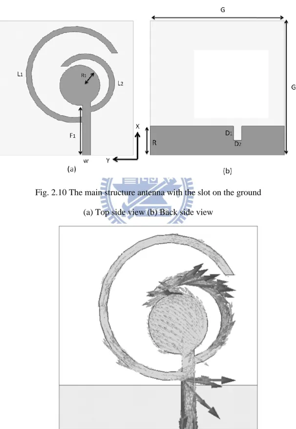
From the previous section, the main structure contained good impedance of 2.5GHz band. Besides return loss, the axial ratio of 2.5GHz band performance is well. In this section, we will create the circular polarization of the 5.2GHz band by using another C shape circular strip and a slot on the ground as shown in Fig. 2.10.
The surface current distribution presents the counterclockwise direction, which is shown in Fig. 2.11. It could be seen in Fig. 2.11, the inner circular strip is close to the middle circular patch. There is coupling effect between the strip and circular patch. It generated larger counterclockwise direction surface current so that 5.2GHz band radiated LHCP.
There are two parameters that we will be discussed: the length of the slot on the ground D1, and the width of the slot on the ground D2. Fig. 2.12 shows the variation
of the 5.2GHz axial ratio with the D1. As D2 is fixed, in this case, we choose D1 =
5.3mm.
Fig. 2.10 The main structure antenna with the slot on the ground (a) Top side view (b) Back side view
Fig.2.12 The variation of the 5.2GHz axial ratio with the D1
C. To Enhance the 5.2GHz Band Left Hand Circular Polarization Gain
In the previous section, we used two circular strips and a slot on the ground to generate 2.5GHz and 5.2GHz bands circular polarization. But at the same time, there is a problem occurred. It is the 5.2GHz band LHCP gain is too small could not satisfiy our requirement. So in this section, we added a circular patch on the back substrate as a reflector. It could collect the beam around the substrate and reflect the beam directly. The structure of the antenna that we added a circular patch on the back substrate is shown in Fig. 2.13. There is one parameter radius of the circular patch is R2, R2 is a
parameter to studied, and its affection with higher band LHCP gain at z axial is illustrated in Fig. 2.14. After optimizing the parameter, the value of R2 = 10.8 mm
Fig. 2.13 Geometry of the proposed antenna (a) Top side view (b) Back side view
2.3 Simulation and Measurement Results for 2.5/5.2GHz Dual-Band Circularly-polarized Antenna
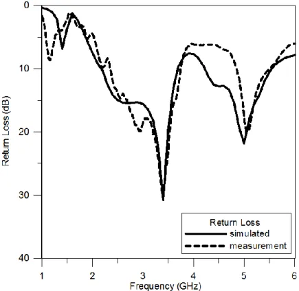
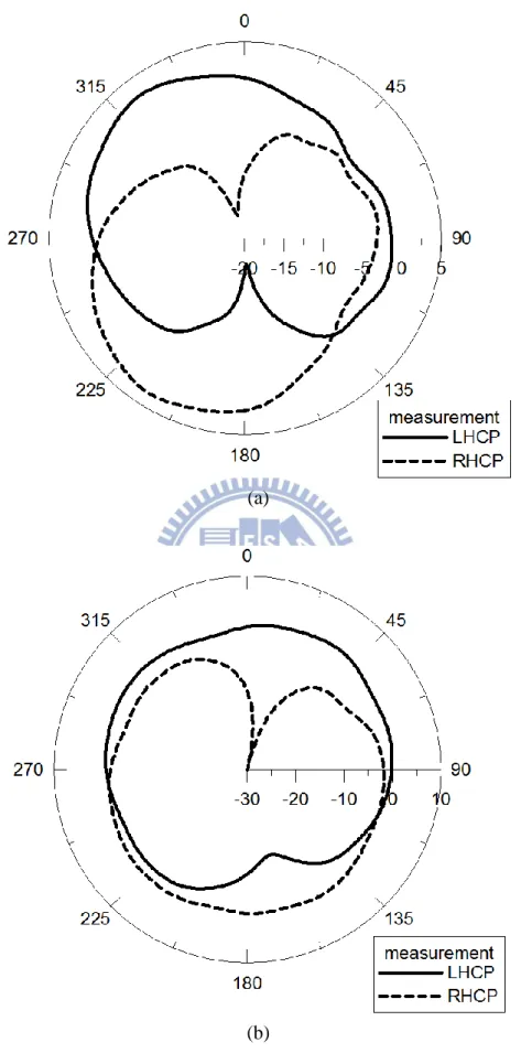
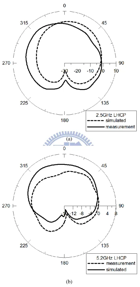
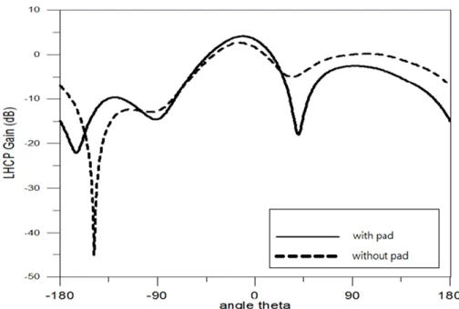
According to the results of the numerical analysis, the optimized parameters of the proposed antenna dimensions are listed in Table2.1. Simulations are carried out using HFSS. The measured and simulated return loss results are shown in Fig. 2.15. The measured results are in good agreement with simulation. The measured results show the (10 dB return loss) impedance bandwidth for the lower frequency is about 1.5 GHz from 2.2 GHz to 3.7 GHz, with a percentage bandwidth of 50%. The higher band radiates from 4.3 GHz to 5.4 GHz with a percentage bandwidth of 23%. The plot of the measured and simulated axial ratio against frequency is shown on Fig. 2.16. The measured 3 dB axial-ratio bandwidth for the lower band is 360 MHz from 2.25 GHz to 2.61GHz, corresponding to about 14.8% with respect to 2.43 GHz, and the measured axial-ratio bandwidth for the higher band is 210 MHz from 5.09 GHz to 5.30 GHz, corresponding to about 4% with respect to 5.2 GHz. Fig. 2.17 shows the measurement of LHCP and RHCP radiation pattern at YZ-plane of 2.5 GHz and 5.2GHz. The comparison of simulated and measurement with LHCP gain was shown in Fig. 2.18. The gain with LHCP in the positive z-direction is about 1.26 dBi at 2.5 GHz, and 3.4 dBi at 5.2 GHz. The circular patch can be considered as a reflector. Without the circular patch on the back of the substrate, the LHCP gain is only 1.56 dBi at 5.2 GHz. The comparison plot is illustrated in Fig. 2.19. The fabricated antenna is shown in Fig. 2.20.
Fig. 2.15. The measured and simulated results for Return Loss curve of the proposed antenna
(a)
(b)
Fig. 2.17 Measurement LHCP and RHCP radiation patterns of the proposed antenna at YZ plane (a) 2.5GHz (b) 5.2GHz.
(a)
(b)
Fig. 2.18 Simulated and measurement LHCP radiation patterns of the proposed antenna at YZ plane (a) 2.5GHz (b) 5.2GHz
Fig. 2.19. The comparison with circular pad on the back of the substrate and LHCP gain at positive z direction.
(a)
(b)
2.4 Conclusion
A novel dual-band circularly polarized microstrip-fed antenna has been designed and fabricated. The antenna generates circular polarization by two circular strips. The proposed antenna can provide wide impedance bandwidths of 50% for lower band and 23% for high band, respectively. The axial ratio bandwidths achieved 14.8% for lower band and 4% for higher band, respectively. The proposed antenna is fabricated on FR4 substrate. The operating dual frequency cover 2.5 GHz and 5.2GHz, so that the antenna could be used in WiMax and WLAN application
C
HAPTER
3
A
2.5/5.2GH
Z
D
UAL
B
AND
MIMO
A
NTENNA
Future wireless communication systems should be capable of accommodating higher data rates than the current systems owing to the advent of various multimedia services. The use of multi-element antennas, such as multiple-input multiple-output (MIMO) antenna systems, is one of the effective ways for improving reliability and increasing the channel capacity.
However, it is very difficult to integrate multiple antennas closely in a small and compact mobile handset while maintaining good isolation between antenna elements since the antennas couple strongly to each other and to the ground plane by sharing the surface currents on them. For a M x N MIMO communication system, the data throughput can be pushed up to K times, K=min(M,N) , that of a single-input single-output (SISO) system, as long as the communication channels linked between the transmitter and the receiver are uncorrelated[11, 20, 21]. The correlation between the channels depends not only on the propagation environment, e.g., multipath effect due to the reflection and diffraction of outdoor buildings or indoor partitions, and also on the coupling between two elements of antennas.
3.1 Basic Theory
3.1.1 Theory of Multiple-Input Multiple-Output (MIMO) Antenna
There are four model of communication system about Single-input single-output (SISO), Single-input multiple-output (SIMO), multiple-input single-output (MISO) and multiple-input and multiple-output (MIMO). And the understanding diagram is shown in Fig.3.1.
One of the main benefits of MIMO systems over traditional SISO systems are their improved capacity and reliability, without increasing transmitted power or
bandwidth. In a MIMO system, the antennas not only have a great impact on the system's received channel capacity, but they also play an important role in system stability.
Antenna diversity is acknowledged as one of the techniques to increase spectrum efficiency in mobile communication systems. It is also recognized that mutual coupling of the antenna degrades the performance of a diversity antenna system. Therefore antenna designers try to design antenna systems that minimize coupling between pens while meeting the input matching requirements. If a uniform random field is assumed and the antenna losses are not considered. Following[22] the envelope correlation for a two-antenna system is computed as:
𝜌
𝑒
=
| 𝐹
4𝜋𝜃,𝜑 ●𝐹
1𝜃,𝜑 𝑑𝛺 |
2|𝐹
1𝜃,𝜑 |
24𝜋
𝑑𝛺 |𝐹
4𝜋𝜃,𝜑 |
2 2𝑑𝛺
(3.1.1)
where F θ, φ is the field radiation pattern of the antenna system when port i is 1 excited, and ● denotes the Hermitian product.
It could be obtained from the S parameters by the following equation [23], such as:
𝜌
𝑒
=
|S
11∗
S
12+S
21∗S
22|
2(1− S
11 2− S
21 2)(1− S
22 2− S
12 2)
(3.1.2)
This induces a mutual-coupling effect that reduces the correlation between antenna elements. If ρe < 0.7 , the diversity gain is not sensitive to the envelope correlation
coefficient. In general, to obtain the characteristic of diversity, ρe < 0.7 at the base
Fig.3.1. The diagram of SISO, SIMO, MISO,MIMO
3.1.2 Theory of Half-Wave Dipole Antenna[19, 24, 25]
In dipole antenna, the very widely used antenna is the half-wave dipole antenna whose structure is shown in Fig. 3.2(a). It is a linear current whose amplitude varies as one-half of a sine wave with the maximum at the center of the half-wave dipole antenna and the current distribution is shown in Fig. 3.2(a). And then the radiation pattern is shown in Fig. 3.2(b). The current distribution is placed along the z-axis and for the half-sine wave current on the half-wave dipole, the current distribution can be written as
( ) sin[ ( )],
4 4
m
I z I z z (3.1.3)
I(z) Im z λ/2 (a) 78o
F(θ)
z
(b) Fig. 3.2 The half-wave dipole(a) Current distribution I(z) and (b) Far-field radiation pattern F(θ)
This current will have the maximum value I at the center (m z0) and will be zero at the ends (
4
z ). According to the current distribution, the far-field radiation pattern can be calculated as
cos( cos ) 2 2 sin r m I e E j r (3.1.4) cos( cos ) 2 2 sin r m I e H j r (3.1.5) 0 E H (3.1.6)
cos[( ) cos ] 2
( )
-sin
F half wave dipole
(3.1.7)
And then we define the antenna directivity, D, which defines as that:
max 4 rad U D P (3.1.8)
In theory, the input power can be radiated totally by antenna. In practical, the antenna has the loss, however, the radiated power will less than the input power. Because of this reason, we define the antenna radiation efficiency, ηr, and the antenna
gain, G, which are defined as
rad r in P P (3.1.9) Note that 0r 1 (3.1.10)
And the antenna gain is
r
G D (3.1.11)
10log dB G G (3.1.12) 10log dB D D (3.1.13)
Gain relative to a half-wave dipole carries the units of dBd. And the unit dBi is often used instead of dB to emphasize that an isotropic antenna is the reference. The relation between the dBi and the dBd is:
2.15
dBidBd (3.1.14)
According to the antenna parameters mentioned above, we can know that the radiation efficiency is the higher the better. That is to say the input power can radiate by antenna almost and then the antenna gain will be higher.
3.1.3 Theory of the Image Theory[19, 24, 25]
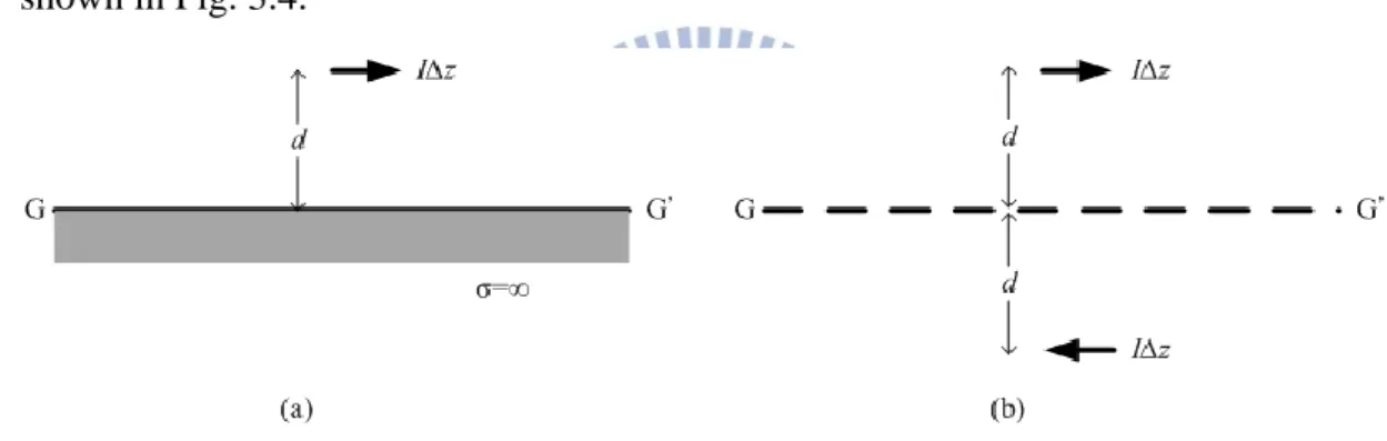
Consider an ideal dipole near a perfect ground plane and oriented perpendicular to the ground plane shown in Fig. 3.3. The uniqueness of the solution to a differential equation (wave equation) plus its boundary conditions introduces an equivalent system that is different below the ground plane (GG’). However, it satisfies the same boundary conditions on the ground plane (GG’) and has the same sources above the plane. Using this equivalent model, the solution will be different for the initial problem which below the plane. However, we can find the same solution for the problem above the ground plane and satisfies the boundary conditions. As a result, the image for this case is equidistant below the image plane and the same direction.
Fig. 3.3 Ideal dipole above and perpendicular to a perfectly conducting ground plane Physical model and (b) Equivalent model using image theory
An ideal dipole oriented parallel to a perfect ground plane has an image that again is equidistant below the image plane. However, the direction is oppositely as shown in Fig. 3.4.
Fig. 3.4 Ideal dipole above and parallel to a perfectly ground plane Physical model and (b) Equivalent model using image theory
The image of a current element oriented in any direction with respect to a perfect ground plane can be calculated by decomposing the element into perpendicular and parallel components, shaping the images of the components, and constructing the image from these image components as shown in Fig. 3.5.
Fig. 3.5 Ideal dipole above and obliquely oriented relative to a perfectly ground plane Physical model and (b) Equivalent model using image theory
3.1.4 Theory of the Monopole[19, 24, 25]
A monopole is a dipole that has been divided in half at its center feed point and fed against a ground plane shown in Fig. 3.6. According to the image theory, if the current distribution over the monopole antenna is equal to the dipole then the electric field of the monopole and the dipole will be the same. However, the image current of the monopole is generated by the ground metal. Hence, the length of the monopole is one-quarter wavelength, which is half of the dipole.
Fig. 3.6 Monopole antenna over perfect ground plane with their image (dashed)
The current and charges on a monopole are the same as on the upper half of its dipole counterpart, but the terminal voltage is only half that of the dipole. The input
1 , 2 , , , , , 1 2 A dipole A mono A mono A dipole A mono A dipole V V Z Z I I (3.1.15)
Where ZA,mono is the input impedance of the monopole and ZA,dipole is for dipole.
Therefore, the radiation resistance of the monopole can be written as:
1 2 , 2 2 , 1 1 , 2 2 , 1 2 dipole mono r mono r dipole A mono A dipole P P R R I I (3.1.16)
Where Rr,mono is the radiation resistance of the monopole and Rr,dipole is for dipole.
The radiation pattern of the monopole above a perfect ground plane is the same as a dipole. However, a monopole fed against a perfect ground plane radiates one-half the total power of a similar dipole in free space. Because of the reason, it is leading to a doubling of the directivity:
1 , 2 , 4 4 2 mono dipole A mono A dipole D D (3.1.17)
Where Dmono is the directivity and Ddipole is for dipole.
3.1.5 Theory of the Defected Ground Structure[26]
In recent years, there have been several new concepts applied to distributed microwave circuits. One such technique is Defected Ground Structure or DGS, where the ground plane metal of a microstrip (or stripline, or coplanar waveguide) circuit is intentionally modified to enhance performance. The name for this technique simply means that a “defect” has been placed in the ground plane, which is typically
considered to be an approximation of an infinite, perfectly-conducting current sink. Of course, a ground plane at microwave frequencies is far removed from the idealized behavior of perfect ground. Although the additional perturbations of DGS alter the uniformity of the ground plane, they do not render it defective.
3.1.6 Modeling of Defected Ground Structure (DGS) [26]
A defect indeed changes the current distribution in the ground plane of a microstrip line, giving rise to an equivalent inductance and capacitance. Thus a DGS behaves like an L-C resonator circuit coupled to the microstrip line. When an RF signal is transmitted through a DGS-integrated microstrip line, strong coupling occurs between the line and the DGS around the frequency where the DGS resonates.
Obviously, it happens of the transmitted signal covers the resonant frequency of the DGS, and most of the signal is stored in its equivalent parallel LC resonator. This indirectly indicates the bandstop feature of a defect in ground plane. The LC parameters are determined by the shape and size of the defect geometry.
A quantitative analysis is necessary to obtain an efficient design specified for different frequencies. An equivalent circuit may help one on this regard. Alternatively, a commercial full wave simulator may be used to characterize a circuit with DGS and to optimize it on a trial and error basis. But this is a time-consuming process particularly when a large structure or a large number of units are to be dealt with. Therefore, efficient modeling using equivalent circuit appears to be a useful solution to handle this issue in a simplified way.
3.1.7 LC and RLC Equivalent Circuit Modeling[26]
The transmission line model, discussed above for simple slot DGS, needs to evaluate the impedance Z0slot. Since this parameter critically depends on frequency, it
of representing a DGS in terms of equivalent parallel LC and RLC circuit has been explored as discussed below.
Fig. 3.7 Side view of Dumbbell-shaped DGS[26]
Fig. 3.8 Top view of Dumbbell-shaped DGS[26]
A simple example is given using a dumbbell-shape DGS shown in Fig. 3.7 and Fig. 3.8. The larger rectangular defect on either side of the line which causes effective series inductance L and the narrow slot beneath the line produces a gap capacitance C in parallel with L, as shown in Fig. 3.9. Once the equivalent L and C values are known, the determination of the DGS characteristics is straightforward.
Fig. 3.9 LC equivalent circuit of single cell dumbbell-shaped DGS
Fig. 3.10 One-pole Butterworth prototype Low Pass Filter
The extraction of the equivalent L and C value [27] is described below. An EM simulator may be employed to determine the S-parameters. For the dumbbell-shaped DGS in Fig. 3.7, the attenuation pole is located at 8 GHz with 3dB cut-off at 3.5GHz. The result resembles the response of a single pole low pass filter and as such cab be fitted with the correlates the Butterworth elements with the unknown L and C values. The reactance of the equivalent circuit of Fig. 3.9
X
LC=
1 ω0 ω0 ω−
ω ω0 (3.1.18)X
L= ω
1Z
0g
1 (3.1.19)where ω1 is the normalized angular resonant frequency. Z0 is the input and output
port impedances, and g1 is the "prototype element" as described in[28].Eq. (3.1.18) and Eq. (3.1.19) at the cut-off frequency, we have,
X
LC|
ω=ωc=X
L|
ωc=1 (3.1.20)C =
ωc Z0g1 1 ω02−ωc2 (3.1.21)L =
1 4π2f02C (3.1.22)The LC modeling does not account for any losses caused by radiation or conductor dielectric losses. A more realistic model takes an equivalent loss resistance R into account. This loss resistance R can be extracted from simulated S11 employing
the following relation[29]:
R =
2Z0 1 |S 11 ω |2−(2Z0 ωC− 1 ω L )2−1 (3.1.23) where,S
11ω =
Zin−Z0 Zin+Z0 (3.1.24)and the equivalent Land C are expressed in Eq. (3.1.21) and Eq. (3.1.22) , respectively.
3.2 2.5/5.2GHz Dual Band MIMO Antenna Design
3.2.1 Design 2.5/5.2GHz Dual Band SISO Antenna
In this section, we designed a 2.5/5.2GHz dual band SISO antenna firstly. The geometry of the proposed antenna with detailed dimensions is shown in Fig. 3.11. It is printed on a FR4 substrate board with dimensions 65 mm × 45 mm. The substrate has a thickness of 1.6 mm and a relative permittivity of 4.4., loss tangent tanδ = 0.002. We designed the dual band antenna with the E shape monopole, and the parameter value is shown in Table.3.1. The simulated result is shown in Fig. 3.12
Fig. 3.11. The main structure of antenna with one element (a) Top side view (b) Back side view
Variable W F a b L1 L2 c D G
Value(mm) 3 46 9 14 6 3 2 45 45
Fig. 3.12. Simulated return loss of one element antenna
3.2.2 Design 2.5/5.2GHz Dual Band MIMO Antenna
In the previous section, we have designed the single element of the antenna with 2.5/5.2GHz. In this section, we used the single element antenna to designed the dual band MIMO antenna system. The two element antenna are positioned symmetric, with the same fabricated parameters, the structure of the antenna is shown in Fig. 3.13. Because of the coupling with the two element, the return loss performance will not as same as the single element antenna return loss performance. To improve the situation, we modified the structure of the two antennas. The main structure of the MIMO antenna dimensions are listed in Table 3.2. The return loss simulated result is plotted in Fig. 3.14. And the isolation between port 1 and port 2 is shown in Fig. 3.15.
Fig. 3.13. The main structure of the MIMO antenna (a) Top side view (b) Back side view
Variable W F a b L1 L2 c D G
Value(mm) 3 46 9 14 8 10 2 45 45
Table3.2 Dimension of The Main Structure of the MIMO Antenna
3.2.2 Using DGS Structure to enhance the Isolation between Two Antenna elements
In the previous section, we designed the 2.5/5.2GHz dual band MIMO antenna. As the Fig. 3.15 shown, we could observe that the antenna isolation between two ports (S12) at 2.5GHz is about -12dB and at 5.2GHz is about -12dB, too. We wanted to
enhance the isolation between two antenna elements to 15dB, even more than 20dB is better. In this section we applied technology named DGS structure; it could improve the isolation, obviously.
The idea of reducing the mutual coupling between two elements antenna is ground slot resonator, which is equivalent to the series RLC resonator. At resonant frequency, the resonator extracts the substrate ground current related to mutual coupling. So, the isolation between two elements antenna is enhanced.
First, we added one slit on the middle of the ground. The structure of the MIMO antenna with the middle slit is shown in Fig. 3.16. It could enhance the isolation at 2.5GHz obviously. The comparison of the middle slit with isolation is shown in Fig. 3.17. Comparison the ground surface current distribution with and without resonator at 2.5GHz is shown in Fig. 3.18. For this parameter sweep, we chose the middle slot S1=18mm.
Fig. 3.16 The structure of the MIMO antenna with the middle slit (a) Top side view (b) Back side view
Fig. 3.18 The comparison surface current distribution at 2.5GHz
With the middle slot on the ground, the isolation at 2.5GHz could be enhanced to 25dB. At the same time, the 5.2GHz band isolation was improved too, as the Fig. 3.17 shown, the isolation could be enhanced to 25dB. Now we will focus on the impedance matching at 5.2GHz. We etched a slit under the element of the antenna, respectively. In this work, we added two symmetric slits from the edge of the substrate 5 mm. There is another parameter S2 could be discussed. In this work, we chose the
S2=12mm, and the width of the slot W2=0.5mm. The proposed 2.5/5.2GHz dual band
MIMO antenna structure is shown in Fig. 3.19. The comparison of return loss with and without the two slits was shown in Fig. 3.20. As a comparison, the simulated isolation without the three slits monopole elements is also plotted in Fig. 3.21. From the figure, it can be seen that by adding the three slits monopole elements the isolation in the operation band is greatly improved, in which S12 decreases from -12 dB to -24
Fig. 3.19 The proposed 2.5/5.2GHz dual band MIMO antenna structure (a) Top side view (b) Back side view
Variable W F a b L1 L2 c D G w1 w2 S1 S2
Value(mm) 3 46 9 17 4.6 14 2 45 45 1 0.5 18 12
Fig. 3.20 The comparison of return loss with and without the two slits
3.3 Simulation and Measurement Results for 2.5/5.2GHz Dual Band MIMO Antenna
The simulated and measured return loss results of the proposed MIMO antenna are plotted in Fig. 3.22 and Fig. 3.23. Due to the symmetric structure, the measured S22 is almost the same as S11. The antenna operates over the range which extends from
2.3 GHz to 2.6 GHz with the impedance bandwidth of approximately 12.2% for the lower band, and 4.8 GHz to 5.4 GHz with the impedance bandwidth of approximately 11.7% for the higher band. And the isolation (S12) of simulation and measurement is
show in Fig. 3.24. The measurement result of isolation is 17dB at 2.5 GHz and 24dB at 5.2 GHz. It is consistency for the higher band, but for the lower band, the simulated is approximately 25 dB, the measurement is only 17dB. One of the reasons is the SMA connector and fabrication imperfections.
The simulated and measured radiation pattern results of port 1 at 2.5 GHz are shown in Fig. 3.25. And Fig. 3.26 shows the pattern of port2 at 2.5 GHz. The simulated and measured radiation pattern results of port 1 at 5.2 GHz are shown in Fig. 3.27. And Fig. 3.28 shows the pattern of port2 at 5.2 GHz. From Eq. (3.1.2) we could calculate the correlation of the MIMO antenna. The result of the correlation is shown in Fig. 3.29. As the Fig. 3.29 shows the correlation coefficient is both smaller than 0.01 at 2.5 GHz and 5.2 GHz. The fabricated MIMO antenna is shown in Fig. 3.30.
Fig. 3.22 The simulated return loss of the proposed MIMO antenna
Fig. 3.23 The measurement return loss of the proposed MIMO antenna
(a)XY
(b)YZ
(c)XZ
Fig. 3.25 The port 1 radiation pattern about simulated and measurement result at 2.5 GHz (a) XY plane (b) YZ plane (c) XZ plane
(a) XY
(b)YZ
(c)XZ
Fig. 3.26 The port 2 radiation pattern about simulated and measurement result at 2.5 GHz (a) XY plane (b) YZ plane (c) XZ plane
(a)XY
(b)YZ
(c)XZ
Fig. 3.27 The port 1 radiation pattern about simulated and measurement result at 5.2 GHz (a) XY plane (b) YZ plane (c) XZ plane
(a) XY
(b) YZ
(c)XZ
Fig. 3.28 The port 2 radiation pattern about simulated and measurement result at 5.2 GHz (a) XY plane (b) YZ plane (c) XZ plane
Fig. 3.29 Computed envelope correlation for the MIMO configuration
(a)
(b)
3.4 Conclusion
In this paper, a three-slit diversity E shape antenna with isolation enhancement using DGS structure of slot resonators for mobile handsets is presented. According to simulated results, a prototype antenna was constructed. The measured results show that the three slit elements are well matched in the whole 2.5 GHz and 5.2GHz band where the 10dB return loss (VSWR < 2) is satisfied. The proposed antenna can provide impedance bandwidths of 12.2% for lower band and 11.7% for high band, respectively. Meanwhile, across the band high isolation (S12 < - 15 dB) is acquired.
![Fig. 2.1 Geometry of microstrip line [14]](https://thumb-ap.123doks.com/thumbv2/9libinfo/8751971.206112/21.892.139.753.326.783/fig-geometry-of-microstrip-line.webp)