覆晶無鉛錫銀銲錫接點之電遷移破壞機制
Failure Mechanism of Electromigration for
Flip-Chip SnAg
3.5Solder Joints
研 究 生:邵棟樑 Student:Tung-Liang Shao
指導教授:陳 智 Advisor:Chih Chen
國 立 交 通 大 學
材料科學與工程學系
博 士 論 文
A DissertationSubmitted to Department of Materials Science and Engineering National Chiao Tung University
in Partial Fulfillment of the Requirements for the Degree of
Ph.D. in
Materials Science and Engineering
September 2005 Hsinchu 30050, Taiwan, ROC
i
覆晶無鉛錫銀銲錫接點之電遷移破壞機制
研究生:邵棟樑 指導教授:陳智博士
國立交通大學
材料科學與工程系所
摘要
本文探討覆晶無鉛錫銀銲錫接點於 150℃的溫度下,不同的通電平均電流密度 1×10⁴ A/㎝ 2 及 5×10³ A/㎝ 2 之電遷移行為及其破壞機制。在上述不同的通電平均流密度狀況 下,觀察到不同的失效模式。當通電平均電流密度為 1×10⁴ A/㎝ 2 時,銲錫接點於晶片 側陰極端或陽極端皆會發生破壞。然而,當通電平均電流密度為 5×10³ A/㎝ 2 時,銲錫 接點破壞只會發生在晶片側陰極端。而為了更進一步瞭解在銲錫接點的電流聚集效應, 利用有限元素法進行 3 度空間之電流密度模擬分析。發現於鋁導線與銲錫接點交接處, 銲錫接點局部電流密度可高達 1.24×10⁵ A/㎝2 。此外亦針對不同通電平均電流密度 1×10⁴ A/㎝ 2 及 5×10³ A/㎝ 2 狀況,實施銲錫接點之溫度與溫度梯度量測。當通電平均電流密 度為 1×10⁴ A/㎝2 時,銲錫接點因焦耳溫升效應溫升值量可高達至 54.5℃,而對應溫度 梯度亦高達365 ℃/cm。焦耳溫升效應在電遷移破壞機制亦扮演一個重要的角色。以下 將針對不同的失效模式,提出對應的電遷移破壞機制。ii
Failure Mechanism of Electromigration for
Flip-Chip SnAg
3.5Solder Joints
Student:Tung-Liang Shao Advisor:Chih Chen
Department of Materials Science and Engineering National Chiao Tung University
Abstract
Electromigration behavior of lead-free SnAg3.5 solder joints was investigated under the average current densities of 1 × 10⁴ A/cm2 and 5 × 10³ A/cm2 at 150℃. Different failure
modes were observed for the above two stressing conditions. When stressed at 1 × 10⁴
A/cm2, damage occurred in both anode/chip side and cathode/chip sides. However, failure happened only in the cathode/chip under the stressing of 5 × 10³ A/cm2. Three-dimensional
simulation of current density distribution by finite element method was performed to provide better understanding of current crowding behavior in the solder joint. The local maximum current density of flip chip solder joint was as high as 1.24×10⁵
A/㎝2
under the stressing of 1 × 10⁴ A/cm2. And the location of the maximum current density occurred in the vicinity of
the Al entrance into the solder joint. In addition, both temperature increases and thermal gradients were measured during the two stressing conditions. The measured temperature increase due to Joule heating was as high as 54.5 ,℃ and the thermal gradients reached 365 ℃/cm when stressed by 1 × 10⁴ A/cm2. Joule heating plays an important role in the failure
mechanism during higher current stressing. Possible mechanisms responsible for the different failure modes are proposed.
iii
誌謝
首先要感謝我的指導老師-陳智教授在這四年來的教導以及生活上的關心與協助, 當我遇到困難時,總能給予適時的幫助與鼓勵,使得問題皆能順利解決。在這段博士班 就學期間從老師身上學到嚴謹的研究態度與對真理的追求的精神。更要感謝杜經寧院士 對於研究方向的啟發與研究方法的指導及建議。讓我對電遷移研究有更深入的瞭解與體 認。並感謝饒達仁老師在溫度量測實驗的指導與協助。使得實驗數據更為完整並對實驗 結果提供有效的佐證。 當然也要感謝許穎超同學,陳義雄,林克謹,邱聖翔,梁世緯,楊慶榮,陳德聖, 黃淵明,周重光學弟在實驗上協助,使得實驗能順利進行。此外也要感謝其他曾給予我 的幫忙的同學及老師。 最後要感謝我的家人,素貞、柏崴與柏鈞,在你們的支持和鼓勵下,讓我能順利完 成研究與學業,並帶給我人生莫大的喜悅。 AcknowledgmentsAt first, I would like to thank my advisor - Professor Chih Chen in over these four years' instruction and assistance. When I encountered difficulty, he always offers me help and encouragement in the right time. Then the problems can be solved smoothly. I also have learned from my teacher for the meticulous research attitude of study and spirit of the pursuit to the truth.
I would like to express my gratitude to professor K. N. Tu at UCLA for helpful discussions of deeper understanding on electromigration research. I also take this opportunity to thank Professor D. J. Yao in National Tsing Hua University for temperature measurement. It is very helpful to have the temperature increase data to explain our experimental results.
Certainly, I would like to express my appreciation to many students for their support. Particularly, the assistance from I. H. Chen, K.C. Lin, Y. C Hsu, S. H. Chiu, S. W. Liang, C. R. Yang, D. S. Chen, Y. M. Huang, and C.K. Chou are greatly appreciated.
Finally, many thanks to Jennifer, my patient and supportive wife, and my sons, Willy and Buddy. They have all brought great joy to my life.
iv
Contents
摘要... i Abstract ... ii 誌謝...iii Contents... iv Figure Captions ... vi List of Tables ... ix CHAPTER I INTRODUCTION ... 11.1 Flip Chip Technology ... 1
1.2 Leadfree Solder ... 6
1.3 Theory of Electromigration ... 6
-1.4 Electromigration in Flip Chip Solder Joints ... - 6 -
1.5 Motivation ... 6
CHAPTER II EXPERIMENTAL ... 13
2.1 Fabrication of Flip Chip Package ... 13
-2.2 Stressing Conditions of Electromigration Test ... - 13-
2.3 Temperature Measurement by Infrared Microsscopy ... - 14 -
2.4 Microstructure Examination ... - 15 -
CHAPTER III SIMULATION ... 18
3.1 3D Current Density Simulation of Flip Chip Solder Joints under Current Stressing ... 18
CHAPTER IV RESULTS ... 26
-4.1 Microstructure of Flip Chip Solder Joints ... - 18 -
4.2 Temperature Measurement of Solder Joints under Current Stressing ... - 21 -
4.3 3-D Current Density Simulation of Flip Chip Solder Joints ... - 21 -
CHAPTER V DISCUSSION ... - 30 -
5.1 Electrical: effect of current crowding on electromigration ... - 26 -
5.2 Thermal: effect of Joule heating on electromigration ... - 27 -
5.3 Chemical: effect of IMC formation on electromigration ... - 28 -
CHAPTER VI CONCLUSIONS ... - 30 -
v
Figures ... - 31 -
Tables ... - 31 -
vi
Figure Captions
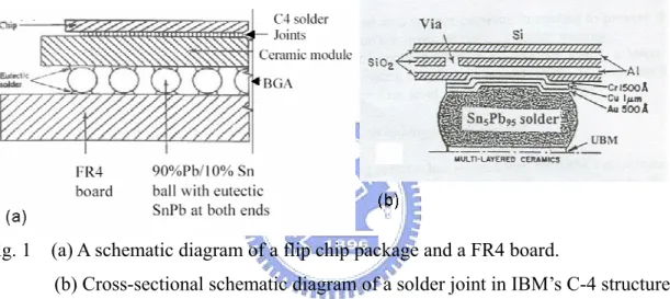
Fig. 1 (a) A schematic diagram of a flip chip package and a FR4 board.
(b) Cross-sectional schematic diagram of a solder joint in IBM’s C-4 structure. Fig. 2 A schematic diagram depicting the wire-bonding packages and flip-chip packages. Fig. 3 A schematic diagram depicting various flip chip technologies.
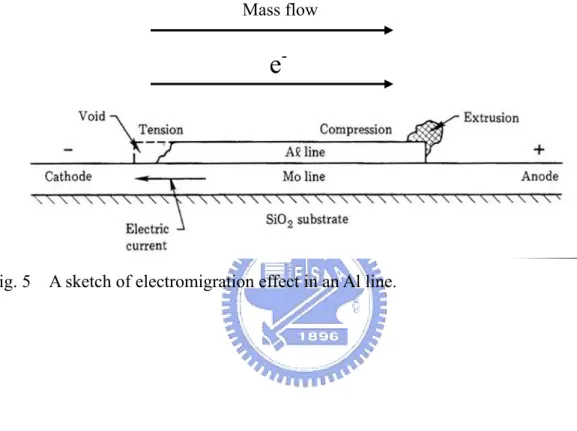
Fig. 4 (a) A schematic diagram of a bumped die. (b) SEM image of a bumped die. Fig. 5 A sketch of electromigration effect in an Al line.
Fig. 6 Electromigration in Al stripe of different lengths [16].
Fig. 7 (a) Schematic diagrams of cross-sectional view showing the structure of a SnAg joint.
(b) Schematic diagrams of flip chip solder joints under current stressing. The directions of electron flow are indicated by arrows in the figure. Fig. 8 (a)-(d) Schematic diagrams of wafer bumping process.
Fig. 9 Schematic diagrams of flip chip process.
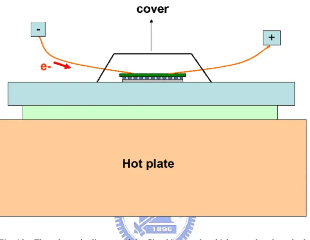
Fig. 10 The schematic diagram of the flip chip sample was placed on the hot plate during current stressing.
Fig. 11 (a) Schematic diagram of Bump 1, in which 97% of the solder remains.
(b) Schematic of experimental setup during temperature measurement of the flip chip package
(c) Schematic of experimental setup during temperature measurement for flip chip package with a Cu heat spreader attached to chip side.
Fig. 12 The treatment process of the plane-view sample.
vii
Fig. 14 The meshed 3-D Finite element model of the flip chip solder joint. Fig. 15 (a) Cross-sectional SEM image of an as-prepared SnAg solder joint.
(b) Cross-sectional SEM image of a SnAg joint aged at 150°C for 20 hours. Fig. 16 Plane-view SEM images showing the morphology of contact openings on the chip
side for (a) an as-prepared SnAg solder joint; (b) a SnAg joint aged at 150°C for 20 hours. Ternary compounds of Ni, Cu, and Sn were found after the aging. Fig. 17 Cross-sectional SEM image after the current stressing of 1 × 10⁴ A/cm2 at 150°C
for 22 hours, (a) for Bump 2, (b) for Bump 1. Voids formed on both the cathode/chip and anode/chip sides.
Fig. 18 Elemental EDS mappings of Ti, Cr, Cu, and Ni for the bump pairs in Figure 5. Ni and Cu atoms accumulated on the anode/chip side.
Fig. 19 Plane-view SEM images depicting the morphology of the contact openings after the stressing of 1 × 10⁴ A/cm2 at 150°C for 22 h. (a) on the anode/chip side, (b) on the cathode/chip side. IMCs formed on both sides.
Fig. 20 Cross-sectional SEM images for the joints after current stressing of 5 × 10³ A/cm2 at 150°C for 218 h (a) for bump 2, in which electrons drifted downward. (b) for the enlarged image on the cathode/chip side.
Fig. 21 Plane-view SEM images showing the morphology of the contact openings after stressing by 5 × 10³ A/cm2 at 150 °C for 218 h. (a) on the anode/chip side, (b) on the cathode/chip side. Failure occurred at the cathode/chip side.
viii
°C. The temperature increase due to the current stressing was 54.5 °C; (b) the corresponding temperature profile along the dashed line in (a), showing a thermal gradient of 365°C /cm across the joint.
Fig. 23 (a) The 3-D current density distribution in the solder joint with the Ti/Cr-Cu/Cu thin film UBM. (b) The current density distribution at the Z-axis cross-section in (a). The white dotted lines show the five cross-sections examined in this study.
Fig. 24 The 3-D current density distribution at the different cross-sections (a) cross-section Y1, which is located inside the UBM; (b) cross-section Y2, which is the IMC layer; (c) cross-section Y3, which is the top layer of the solder connected to the IMC formed between the UBM and the solder; (d) cross-section Y4, which has the largest diameter in the joints; (e) cross-section Y5, which has a smaller diameter due to solder mask process; (f) cross-section Y6, which is situated at the bottom of the solder joint.
Fig. 25 (a) Plane view SEM image of the morphology on the contact opening of the chip/cathode side of the solder joint after the current stressing by 0.567 A at 150℃ for 20hrs. (b) The simulated current density distribution in the top layer of the SnPb solder. The IMC/UBM dissolved much faster near the entrance of the Al trace into the solder joint, where it had much higher current density.
Fig. 26 The crowding ratios inside the solder joint for the five UBM structures at different cross-sections.
ix
List of Tables
Table 1. The melting point and composition of binary solders. Table 2. Common IMCs of Sn.
Table 3. Wafer bumping process. Table 4. Flip chip process.
Table 5. The resistivities of the materials used in the simulation models.
Table 6. The maximum current densities and the crowding ratios at different cross-sections for the five models.
- 1 -
Chapter I Introduction
1.1 Flip Chip Technology
To connect the electrical circuit in a chip to the outside world for higher performance and better reliability is the main concern in the microelectronic packaging. Wire bonding technology has been used for a long time. The wire bonding technology has limited capacities of input/output (I/O) interconnection density, transmit speed and heat dissipation. It fails to meet the requirements of I/O and performances for the high-end devices. The requirement in the next ten years is proposed in International Technology Roadmap for Semiconductors by Semiconductor Industry Association. [1] Hence, the trend in microelectronic packing is to a wider use of solder bumping. A high I/O density can be achieved by making a large number of tiny solders into an area on a chip surface as I/O interconnections by solder bumping technology. For example, we can have 10,000 bumps/cm2 for 50µm bumps in diameter and 100µm bump pitch. The RC delay of solder bump interconnections is smaller than that of wire bonding interconnections as well as the parasitic capacitance. Therefore high electrical speed can be obtained for the flip chip products. Furthermore, the heat dissipation of flip chip structure is more efficient than that of wire bonding structure. The thermal resistance of solder joints is at least ten times less than that of wire bonding.
The flip chip technology was derived from IBM’s C-4 (controlled-collapse chip connection) technology in the early 1960s. The so-called C-4 technology deposited solder bumps deposited on I/O pads of chips. Then the chip was aligned and flipped on the ceramic substrate. The solder bumps were melted and self-align reaction resulted from the surface tension of the molten solder between the chip and the substrate during the reflow process. At the same time, the solder joints between the chip and the substrate formed simultaneously.
- 2 -
IBM adopted the 5wt%Sn/95wt%Pb solder, which has solid and liquid temperatures of 320℃. IBM used the ceramic substrate, which has a similar coefficient of thermal expansion (CTE) with the chip material, in order to reduce the residual stress due to CTE mismatch. The schematic diagram of C-4 structure is shown in Fig. 1.
The Flip Chip technology is better than traditional wire bonding technology for excellent performances of high I/O density, high speed and high thermal heat dissipation. Wire bonding must be done on the periphery of the chip. Even if we can use 50µm wire with 50µm spacing, we can only have about 400 I/Os on the periphery of a 1 ㎝2 chip. The only feasible way to provide such a high I/O density pads is to adopt flip chip bonding. There are 10,000 solder balls that can be deposited or electroplated on 1cm2 chip. Figure 2 shows that the schematic diagram of wire-bonding packages and flip-chip packages.
Besides, the metal bumps have shorter interconnect length between the chip and the substrate than wire bounding interconnects and provide better efficient heat dissipation path also. Further more, metal bumps have smaller parasitic capacitance than wire bonding interconnects. Therefore, strong attentions to flip chip technology were paid by semiconductor packaging industry recently. A lot of flip chip packages were manufactured for different kind of high I/O pin counts, high speed and high power devices. The flip chip technology has become one of the most important applications in semiconductor packaging industry.
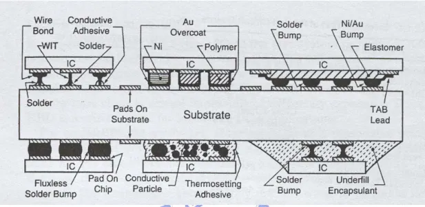
In general, flip chip is defined as to mount a chip on a substrate. In another words, the chip surface (active area or I/O side) is facing the substrate. Various flip chip methods with different materials are developed, for example, there are metal bumps, fluxless solder bumps, tape-automated bonding, wire interconnects, isotropic and anisotropic conductive adhesives, compliant bumps, and pressure contacts. [2] Various flip chip technologies is displayed in
- 3 -
Fig. 3.
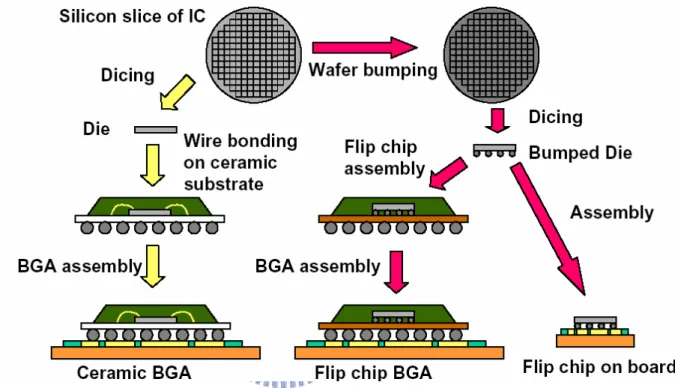
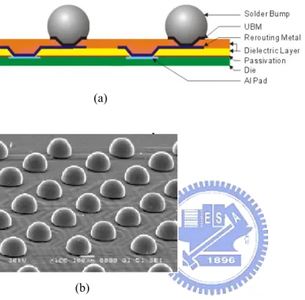
The wafer metal bumping is one of the most important methods for the flip chip technology. Several wafer bumping processes, such as evaporation, plating, printing, and ball placement, and stud bond bumping etc., are well developed and applied. The under bump metallization (UBM) defines the region of terminal metallurgy on the active surface of the chip. Solders are wetted with the UBM, which usually consists of three layers: adhesion and/or barrier layer, wetting layer, and protective layer. The schematic diagram and SEM image of a bumped die is shown in Fig. 4.
The quality of UBM systems used for solder bump flip chip applications was investigated from the viewpoints of thermal stability, corrosion-resistance, and thermal-mechanical reliability. [3] Thermal stability was verified by multiple solder reflow passes and high temperature storage tests. To form a solder joint, the solder must react with the wetting layer of UBM, typically Cu or Ni. One of the most challenging issues is how to control the wetting reactions. This is because many kinds of UBM use thin metal films on a chip. During wetting reactions, the molten solder can consume a 1 micron thick Cu thin film in less than one minute. In general, the solder joints are needed to go through several reflows or wetting reactions during manufacturing a flip chip device. When the thin film UBM is consumed, the interface of the solder joint becomes much weakened mechanically due to spalling of IMC into the solder. [4] The spalling is a challenging reliability issue for flip chip lead-free solder joints. Regarding corrosion-resistance and thermal-mechanical reliability issues, the electronic industry has introduced epoxy underfill between the chip and the substrate. The underfill can improve the corrosion-resistance and redistribute the thermal stress due to the large difference in coefficients of thermal expansion between chip (α=2.6 ppm/C) and organic substrate (α=18 ppm/C).
- 4 -
electromigration (EM) of solder joints under high electrical current stressing has attracted much attention. Solder bump pitch has decreased rapidly, in turn the contact area of the solder bumps and the diameter of under bump metallization (UBM) decrease rapidly too. On the other hand, the operation current for the bumps keeps increasing, resulting in a dramatic rise of the current density in the solder bump. [5-7] Therefore, Joule heating in the older joints becomes a reliability issue. [8] Since electromigration is the result of a combination of thermal and electrical effects on mass migration.
1.2 Lead-Free Solder
With increasing environmental concerns, the microelectronics industry is paying greater attention to lead-free solder alternatives. Furthermore, Pb-containing solders may contain some amount of Pb210 isotope. It decays to Bi and emits alpha particles during the decay.
The electrons and holes formed while these particles pass through a Si device. Before these charge carriers recombine, they may affect the charges stored in the capacitors of the memory device. The “soft error” failure occurs due to the change of the charges stored in the capacitors [9]. Pb-free solder is one of the solutions to prevent these problems.
In Japan, all major consumer electronic manufacturers (SONY, TOSHIBA, and NEC etc.) request to phase in lead-free products in 2005. In the United States, there are four bills pending in the Congress. Europe has the Waste Electrical and Electronic Equipment (WEEE) directive to stop the use of Pb in consumer electronics in 2006. The National Electronics Manufacturing Initiative (NAMI) has a lead-free assembly project to address solutions of lead-free electronics manufacturing.
Recently, most lead-free solders are alloys of Sn. It is preferred to use eutectic solder alloy in flip chip products. The reason is that the flip chip solder joint will melt or solidify at the same eutectic temperature due to the single melting point of the eutectic alloy. For the
- 5 -
binary alloys, Sn-Ag, Sn-Cu and Sn-Au are eutectic alloys of Sn and noble metals (Cu, Ag, and Au). There are other alloying elements such as Bi, In, Zn, Sb, and Ge. In general, the melting point of a lead-free solder is higher than that of eutectic SnPb, except SnBi and SnIn. Typically, the corresponding reflow temperature will be higher about 30℃ than melting temperature. The dissolution rate and solubility of Cu and Ni in the molten solder molten solder increase with the reflow temperature. Consequently, the rate of IMC formation with Cu and Ni increases for the higher reflow temperature during solder reflow process.
Among the binary solder alloys, Sn-Ag eutectic solder is one of the most promising alternatives for flip chip packages. It is easier to manufacture SnAg3.5 solder bumps on a wafer than tenary eutectic solder bumps by electrical plating. The SnAg3.5 solder bumps manufactured by printing technology is also commercially available. Besides, the tenary eutectic SnAgCu alloy has received much attention. The melting points and compositions of various lead-free solders and Sn-Pb solder are shown in Table 1. [10]
Basically, they are based on the binary eutectic Sn-Ag, Sn-Zn, Sn-Cu, or Sn-Bi alloy. The most promising ones are eutectic Sn-Ag and Sn-Ag-Cu. Some element has the specific features for application. For example, Indium (In) is effective in reducing the melting temperature of SnAg solder. The eutectic temperature of the Sn-Ag-In system is about 113℃.[11] However, In is too scarce and too expensive to be considered for mass production applications. Zinc (Zn) is cheap and readily available, but it quickly forms a stable oxide. The oxide formation resulted in very poor wetting behavior during manufacturing. Bismuth (Bi) has very good wetting and physical properties. However, the availability of Bi could be limited and the primary source of Bi is a by-product in Pb refining. By restricting the use of Pb, much less Bi will be available.
To use the lead-free solders, we must consider what are the key concerns in the manufacturing and application of flip chip packages. The first challenging issue is to control
- 6 -
the wetting reaction for forming a solder joint. Afterwards, the solder joints will go through several wetting reactions or “reflows” to produce a flip chip package. The molten solder can consume a micron thick Cu thin film during wetting reactions. The shear force and the interface of the solder joint becomes much weakened due to the phenomenon of “spalling” while the UBM is consumed quickly. Spalling was observed in eutecic SnAgCu solder on Cu/Ni(V)Al thin film. [12] Lead free solders solder always contains a high concentration of Sn. It can consume all the Cu film very quickly, resulting in ripening and spalling of the Cu-Sn compound [13]. Thus, the solder joint weakened because of poor adhesion between the solder and the remaining UBM layer.
The compatibility of UBM and lead free solders needs to be considered for reaction of forming a solder joint of the flip chip packages. The combinations of UBM and lead free solders will influence IMC to be formed after reflow. The morphology and composition of IMC may impact the mechanical property and reliability of solder joints. Some common IMCs formed by Sn and other elements were showed in Table 2.[14] Therefore, the solder-UBM reaction is a critical concern of manufacturing of flip chip packages.
1.3 Theory of Electromigration
The mass transport by the electric field and charge carriers is called electromigration. The transport of current can displace the ions and influence the transport of mass at a high current density (above 102 A/cm2 ). The conduction electrons are free to move in the metal and scattering interactions occur due to phonon vibration. The electrical resistance and joule heating resulted from the scattering interactions. The scattering does not enhance displacement of the ion, or it has no net effect on the diffusion of the ion when the electric current density is low. However, the scattering enhances atomic displacement in the direction of electron flow at a high current density (above 10 4 A/cm2).[15] The enhanced
- 7 -
atomic displacement induced the accumulated effect of mass transport under the influence of electric field.
Electromigration is a mass transport driven by an electric field. The direction of mass transport is the same as that of electron flow. The phenomenon of electromigration can be illustrated by the response of short conducting lines under a high current density. Fig. 5 shows electromigration of Al line, which is a typical Blech structure.[16] Electromigration occurs and leads to extrusion at the anode and voids at the cathode.
Electromigration results from the combination of thermal and electrical effects on mass motion. If the conducting line is kept at a very low temperature (e.g., liquid nitrogen temperature), electromigration cannot occur because there is no atomic mobility. The contribution of thermal effect can be recognized by the fact that electromigration in a bulk metal occurs at about three-quarters of its melting point in absolute temperature. Electromigration in a polycrystalline metallic thin film occurs at about one-half of its melting point in absolute temperature. At these temperatures, the atoms are undergoing random walks in the lattice of the bulk and in the grain boundaries of the thin film, respectively. The atoms participate in electromigration under the applied field.
The driving force for electromigration consists of the “electron wind force” and the “electrostatic field force”. The electron wind force refers to the effect of momentum exchange between the moving electrons and the ionic atoms when an electrical current is applied to the specimens [17]. The electron flow might act as a “frictional” force on the diffusing atoms. The “frictional” force is commonly called “electron wind force.” Therefore the total driving forces exert on the moving ion can be given by
wind el field
driving
F
F
- 8 -
The atomic mass transport driven by the electric field and charge carriers [16]. In an electric field E, the force on an electron is eE, and the force on an ion is Z*eE. Equation (1) can be written as:
………… (2) Where:
e is the charge of electron. E is the electric field.
Z*el is the nominal valence of the diffusing atom.
Z*wd is the effective charge number for the electron wind. Z*wd > Z*el Atoms move in the same direction as e-.
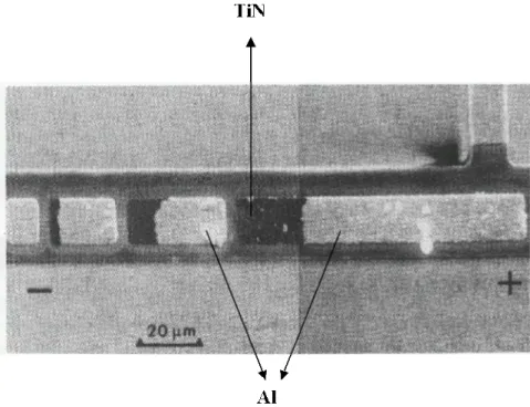
It was found that no electromigration occurs below a certain length due to the back stress generated in the stripe. When the stripe is very short, the vacancy gradient can be large enough to prevent electromigration. Because stress gradient produced by the compressive stress at the anode, it can push Sn atoms back to cathode. The back stress induced by electromigration and it is a steady state stress [18-19]. In electromigration, the anode in a Blech structure is under compression and has less equilibrium vacancies, and the cathode is under tension and has more equilibrium vacancies. Thus, the stress gradient produces a vacancy gradient and leads to a flux of vacancies to go from the cathode to the anode. The direction of the gradient is against the atomic flux of electromigration. However, this vacancy flux does not lead to void formation in the cathode [20-21]. Fig. 6 shows the Al stripe after current stressed. The longer the stripe, the less the back stress. There is a critical length below which no electromigration damage occurs. The critical length can be given by
eE Z x= ∆* Ω
∆ σ ………(3)
- 9 -
1.4 Electromigration in Flip Chip Solder Joints
In 1998, Brandenburg and Yeh reported the observation of electromigration failure in flip chip eutectic SnPb solder joints, stress under 8x10³ A/cm2 at 150 ℃ for a few hundred hours. [22] The important findings are void formation at the cathode and Pb accumulation at at the anode of the solder joint. In the recent study, it is found that electromigration failure in flip chip SnAg3.5 solder joints occured under stressing of 3.58x10⁴ A/cm2 at 120 ℃ after 20
hours. [23] Metal atoms move in the same direction as the electron current flows and the subsequent void accumulation at cathode UBM induces failure. T. Y. Lee and K. N. Tu reported the finding of the squeezed-out IMC at the anode side of flip chip SnAg3.8Cu0.7 solder joints after current stressing at 120 ℃ with 1.5 A. [24] If the lead-free solder joint is confined by under fill, no surface relief can take place, then the build of compressive stress at the anode may crack the passivation on the Si surface. It plays an important role in the failure of electromigration for flip chip lead-free solder joints.
The two-dimensional simulation of current crowding phenomenon in flip chip solder joints is reported by Everett et al. [5] At the contact interface between the metal line and flip chip solder joint, a very large current crowding occurs and it causes a unique and fast electromigration failure in the solder joint. A study of electromigration in three-dimensional (3-D) flip chip solder joint using numerical simulation of heat flux and current density has also been reported. [25] The solder joint is simplified as a cylinder. The current density distribution in the solder joint changed as the direction of the current flow and metal trace thickness changed.
Roush and Jaspal reported thermal migration in Pb-In solder alloy at a thermal gradient of 1200 /cm. [℃ 26] The joule heating during current stressing may maintain a thermal gradient in the solder joint. A three-dimensional coupled electrical thermal finite-element simulation of a flip chip module is reported by Hua Ye et al. [8] A thermal gradient of
- 10 -
1500℃/cm under 1.3x10⁴ is predicted in the simulation which exceeds the gradient reported
by Roush. The real temperature gradient in the solder joint may not be exactly 1500℃/cm due to the discrepancy between the simulation model and real module. The FE simulation result supports the existence of the thermal gradient within the solder joint. Besides electromigration, thermomigration is also an important reliability concern for the flip chip solder joint under high current stressing. Thermomigration may assist or counter electromigration depending on the direction of thermal gradient and electric field.
1.5 Motivation
With increasing environmental concerns, the microelectronics industry is paying greater attention to lead-free solder alternatives. One of the most promising alternatives is SnAg3.5 solder for flip chip packages, and manufacturing of SnAg3.5 solder bumps on a wafer by electrical plating or printing technology is now commercially available. Furthermore, the input/output (I/O) pin count of flip chip products has dramatically increased recently. In addition, bump pitch has decreased rapidly, so, the contact area of the solder bumps and the diameter of under bump metallization (UBM) continuous to shrinking. Therefore, electromigration (EM) of the Pb-free solder bumps has become an important issue, [4, 15] and it needs urgently to be studied.
The previous studies on electromigration of flip chip solder bumps were mainly focused on eutectic SnPb solders. [22, 27] Current crowding effect on the cathode/chip side was proposed to be responsible for the failure at the cathode/chip side of the SnPb bumps. Recently, efforts have been made on the electromigration of Pb-free solder bumps. [23-24] The current-crowding induced by electromigration still plays a crucial role in the failure of the joints. Two-dimensional simulation and a 3-D simplified heat flux cylinder model have been
- 11 -
carried out to depicting the current density distribution in solder bumps. [5, 25] However, the real 3-D current density simulation of the flip chip solder joint, including UBM and IMC layer, was not carried out. In this dissertation, a three-dimensional current density finite-element simulation of the flip chip solder joint was performed to analysis the current density distribution inside the whole solder joint. The simulation modeling is created by considering the real 3-D geometry of the flip chip solder joint, UBM and IMC layer. The simulation result depicts the location of maximum current inside the solder joint and the current crowding ratio. The UBM effect on current density of flip chip solder joint is also examined.
In addition, thermomigration due to the thermal gradient in the flip chip solder joints is considered to account for void formation on the anode/chip side. [8] Regarding the temperature measurement of flip chip solder joints during current stressing, only thermal couple was adopted to measure the die surface in the previous study. The space resolution of the thermal couple is not enough to measure the temperature of the flip chip solder joint of 100 um in diameter. And the attachment of a thermal couple on the flip chip sample induces additional heat sink and heat conduction path, which results in disturbing of the temperature of the flip chip joint. In this research, infrared microscopy was successfully used to measure the temperature distribution inside the flip chip solder joint under current stressing at the first time for electromigration research. The QFI thermal infrared microscopy, which has 0.1℃ temperature resolution of and 2 µm spatial resolution, can detect the temperature distribution of the flip chip solder joint without additional heat disturbing by the remote detection. It is very help to explain the experimental results and failure mechanism.
However, concerning flip chip SnAg3.5 solder joint on Ti/Cr-Cu/Cu UBM and Ni(P)/Au
pad, little research has been made on the failure mechanism due to electromigration. We found that three failure modes occurred in this system when the solder joints were stressed by
- 12 -
5 × 10³ A/cm2 and 1 × 10⁴ A/cm2. The goal of this disseration is to investigate the
electromigration mechanisms of flip chip SnAg3.5 solder joints. Since electromigration is the
result of a combination of thermal and electrical effects on mass motion, a three-dimensional simulation on current density distribution was performed to provide better understanding of the current crowding behavior in the solder joints. Furthermore, temperature increases and temperature gradients due to the current stressing inside the solder joint were measured to examine the thermal effect on the migration of atoms. Possible failure mechanisms responsible for the three failure modes are proposed.
- 13 -
Chapter II Experimental
2.1 Fabrication of Flip Chip Package
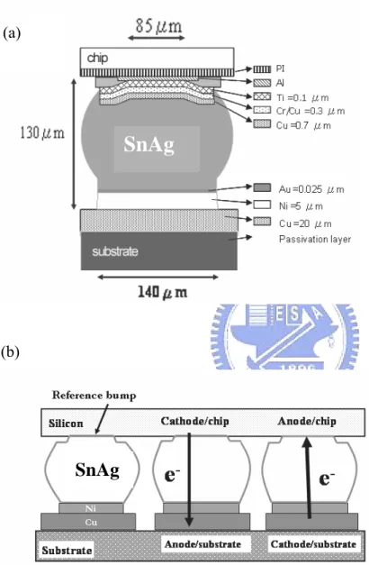
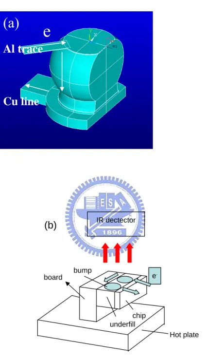
The flip chip package was designed to have special circuit to do electromigration experiment. A pair of solder joints can be easily input current by pad on the substrate. A schematic diagram of the solder joint of the flip chip sample is illustrated in Fig. 7(a). The chip size was 9.5 × 6.0 mm with 85μm UBM contact opening and UBM consisted of 0.7μm Cu, 0.3μm Cr-Cu, and 0.1μm Ti. The directions of electron flow are indicated by arrows in Fig. 7(b). BT substrate was employed for the flip chip package.
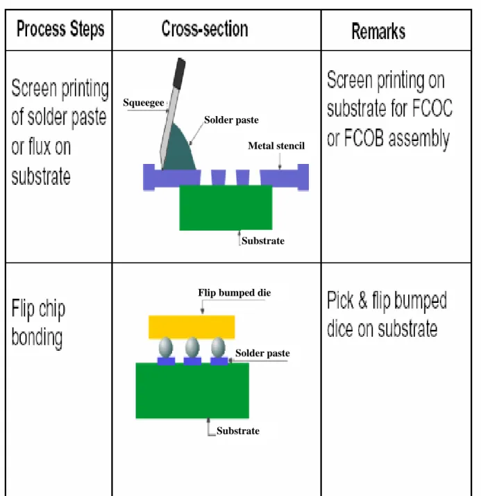
The flip chip packages of SnAg3.5 solder bumps were prepared as follows: Al pad was defined by thin film and photolithography process. Afterwards, rerouting metal circuitSnAg3.5 solder paste was printed and deposited on the UBM pad of the chip. The wafer was reflowed in a nitrogen atmosphere oven at the 250℃ peak temperature and remained above the liquidus temperature for approximately 60 seconds. Then the bumped die sample was prepared after sawing. The wafer bumping process is listed in the Table 3 and illustrated in Fig. 8.
Afterwards, the bumped die was mounted on a BT substrate, on which SnAg3.5 solder paste was printed through metal stencil printing on the metallization pads of the substrate. Then the flip chip sample was reflowed for the second time in a nitrogen atmosphere oven at 250℃ peak temperature for approximately 60 seconds. The flip chip joints were formed after the second reflow. Afterwards, the flip chip package was underfilled. The flip chip process is described in Table 4 and shown in Fig. 9.
- 14 -
2.2 Current Stress Conditions of the Electromigration Test
The flip chip package was stresses under the current density of 1 x 10⁴ A/cm2 and 5 x 10³ A/cm2 at 150℃ hot plat. The schematic diagram of electromigration experiment is illustrated in Fig. 10. The flip chip package was designed with input pads for connecting input current wires. The sample was placed on a hot plat which the temperature was maintained as 150℃. Figure 7(a) displays the schematic diagram of the flip chip solder joint. In this study, we refer the right joint as Bump 1, in which the electron flow goes from the board side to chip side; while the middle joint is Bump 2, in which the electrons migrate from the chip side to the board side. The direction of the electron flow during the current stressing is indicated by the arrows in Fig. 7(b).
2.3 Temperature Measurement by Infrared Microscopy
To measure temperature increase in the solder joints due to the current stressing, a solder joint was polished laterally until the contact opening was visible, with approximately 97% mass of the bump remaining, as shown in Fig. 11(a). Experimental setup of temperature measurement of the flip chip package is illustrated in Fig. 11(b). The current stressing of the specimen was performed on a hot plate in ambient air, which has heating capacity up to 120℃. The specimen was powered by various currents on a hot plate maintained at 70℃. Prior to the current stressing, the emissivity of the specimen was calibrated at 70 ℃ . After the calibration, the bumps were powered by the desired currents. Then, temperature measurement was performed to record the temperature distribution after the temperature reached a stable state. The temperatures in the solder joints were detected by a QFI thermal infrared microscopy, which has 0.1℃ temperature resolution of and 2 µm spatial resolution.
- 15 -
2.4 Microstructure Examination
Microstructure of reference solder bumps and stressed bumps were observed by scanning electron microscope (SEM). The cross-sectional samples were prepared by polishing laterally until the contact opening was visible. In addition to the cross-sectional samples, the plan-view specimens are also prepared to observe failure phenomenon easily. The treatment process of plane-view samples is illustrated in Fig. 12. To make the plane-view specimens for observation by scanning electron microscope, samples were ground either from the substrate side or the chip side there was about 10 µm-thick solder left. Then, an etching solution consisting of glycerin, nitric acid and acetic acid at ratio of 1 : 1 : 1, was used to selectively etch the tin. Thus, the morphology of intermetallic compound (IMC) and the whole contact opening could be observed clearly after the selective etching. Microstructure and composition were examined by a Joel 6500 field-emission SEM and energy dispersive spectroscopy (EDS), respectively.
- 16 -
Chapter III Simulation
3.1 3-D Current Density Simulation of Flip Chip Solder Joints
under Current Stressing
The distribution of current density inside the flip chip solder joint is not uniform due to the current transition from the thin on-chip metal line to the solder joint. Current crowding occurs in the solder joint much more seriously than that in Al and Cu interconnects,[6] and it was found to play a critical role in the electromigration failure of the solder joints.[7] Therefore, two-dimensional (2-D) simulation on current density distribution has been performed to explain the current-crowding-induced failure in flip-chip solder joints.[5] Furthermore, the current density distribution in solder joint has been simulated.[25] However, the current density distribution in the flip-chip solder joints may not be symmetrical in geometry over a specific plane. Thus, a 3-D simulation is needed to provide deeper understanding on current density distribution in the solder joints. In addition, various UBM structures have also been used in the microelectronics industry. However, there is little research done on the current density distribution in the solder joints with different UBM structures. This study employed finite element method to simulate the current density distribution in solder joints with five different UBM structures, including Ti/Cr-Cu/Cu thin film UBM, Al/Ni(V)/Cu thin film UBM, Cu thick film UBM, Ni thick film UBM, and Cu/Ni thick film UBM. This research provides a better understanding on the current density distribution in the solder joints and the correlation of the current crowding effect to electromigration failure time.
3-D current density distribution of flip chip solder joints was investigated in this study. The thin film UBM consisted of 0.1 µm Ti thin film/0.3 µm Cr-Cu/ 0.7 µm Cu UBM. The cross-sectional schematic diagram of simplified flip chip solder joint is shown in Fig. 13. Compared with the flip-chip structure, each layer in the thin film UBM was too thin to be
- 17 -
simulated individually, and thus an effective layer was used to represent the tri-layer structure. In additions, the intermetallic compound (IMC) formed between the UBM and the solder was also considered in the simulation models. The Cu layer was assumed to consume 0.5 µm, and form 1.4 µm of Cu6Sn5 IMC. On the substrate side, Ni3Sn4 IMC of 1 µm was used in the
model for Ni metallization. Layer-shape IMC was used in this simulation for both the Cu6Sn5
and Ni3Sn4. For the UBM consisting of 0.1 µm Ti /0.3 µm Cr-Cu/ 0.7 µm Cu, an effective
layer of 0.6 µm with a resistivity of 13.1 µΩ-cm was used in the simulation, whereas for the 0.4 µm Al/0.3 µm Ni(V)/ 0.4 µm Cu, an 0.7 µm effective layer with 29.5 µΩ-cm was adopted. The resistivity of the materials used in the simulation is listed in Table 5.
A 3-D finite element model was constructed to simulate the current density distribution in the flip-chip solder joints, as illustrated in Fig. 14. A simplified UBM structure with the UBM opening of 120 µm in diameter was used. The contact opening in the substrate side was 144 µm in diameter. A current of 0.567 ampere was applied. The corresponding current density in the Al trace was 1.11 × 10⁶ A/cm2, and the calculated average current densities were
5.01 × 10³ and 3.48 × 10³ A/cm2 for the contact opening of the chip side and of the substrate
side, respectively.
- 18 -
Chapter IV Results
4.1 Microstructure of Flip Chip Solder Joints
Figure 15(a) shows the cross-sectional SEM image of a solder joint without thermal annealing and current stressing. IMCs of (Cu, Ni)6Sn5 were found on the interface of the
solder and the metallization layer in the substrate side. However, there were no obvious IMCs observed in the vicinity of the UBM on the chip side. Figure 15(b) depicts the bump microstructure after thermal annealing at 150℃ for 20 hours. IMCs of (Ni,Cu)3Sn4 formed
at the interface of the solder and the Ni pad in the substrate side after the solid state aging. Furthermore, several large Ag3Sn IMCs and numerous small Ag3Sn particles were observed in
the bulk solder, as seen in the Fig. 15(b). A slight amount of (Cu,Ni)6Sn5 IMC in the solder
joint near substrate side was occasionally observed. Again, no large amount of Cu-Ni-Sn IMCs was seen in the chip side.
To examine the microstructure evolution on the contact opening of the chip side after current stressing, SnAg solder was etched selectively to allow plan-view observation of the contact, which can provide more information for the failure mechanism when the electromigration damage occurs in the UBM. In addition, IMC formation on the contact opening can be clearly observed since the etchant does not etch Cu-Ni-Sn IMCs and the UBM. Figure 16(a) depicts the plan-view SEM image of the contact opening on the chip side when the SnAg solder was etched away, and the whole contact opening can be clearly seen. The inner circle is the contact opening for the solder bump connecting to the Al trace on the chip side. No obvious IMCs were found to attach to the UBM. Figure 16(b) shows the plan view of the chip side that was only thermally annealed at 150℃ for 20 hours. Several IMCs were observed after the thermal annealing, as indicated by the arrow in Fig. 16(b). The EDS results indicated that they consisted of Sn, Ni, Cu and Cr. The Ni atoms may migrate from
- 19 -
the substrate side during the annealing process.
Surprisingly, both the anode/chip and the cathode/chip sides of the SnAg joints may be damaged after the current stressing by 1 × 10⁴ A/cm2 at 150℃. However, damage may occur on both sides, or only on one of them. The current density was calculated based on the area of contact opening on the chip side. In these packages, the contact opening was 85 µm in diameter on the chip side, while 150 µm in diameter for the pad opening on the substrate side. Thus, the current density on the chip side was about 3 times larger than that of the substrate side. Therefore, electromigration damage generally occurs on the chip side. Figure 17 shows the cross-sectional SEM images of the bump pairs after the current stressing at 1 × 10⁴ A/cm2 at 150℃ for 22 hours. Open failure occurred after the current stressing
and voids formed near the chip sides of the bump pairs. On the anode/chip side, as shown in Fig. 17(a), voids/cracks can be observed near the UBM. In addition, IMCs of (Ni, Cu)3Sn4
can be detected below the UBM, as indicated by one of the arrows in the figure. On the cathode/substrate side, the IMCs also grew larger. Some IMCs inside the solder were determined to be (Cu, Ni)6Sn5. On the cathode/chip side, as shown in Figure 17(b), voids
are also found inside the solder below the UBM. Furthermore, the voids on right side are bigger than those on the left side. The IMCs on the anode/substrate side grew bigger. Elemental EDS mappings of Ti, Cr, Cu, and Ni were performed for the bump pairs, as shown in Figure 18. The UBM layers for both bumps were damaged, and Ni and Cu atoms were detected as accumulating in the solder near the center of the UBM on the anode/chip side. The Ni atoms had migrated from the substrate to the chip side in the same direction of electron flow. Since thermal gradient in the joint drove atoms from the chip side to the substrate side, the electrical field could be the major driving force to migrate Ni atoms from the substrate side to the chip side. However, the Cu atoms may have come from the UBM either on the chip side or from the substrate side, since part of the Ni layer in the substrate
- 20 -
side was damaged.
Plane views for the contact opening on the chip side were prepared to investigate the failure mechanism. Figure 19 shows the microstructures of the contact openings of another bump pair that failed after the current stressing of 1 × 10⁴ A/cm2 at 150℃ for 22 hours. Both the contact openings for the anode/chip and the cathode/chip sides are clearly shown after the selective etching of Sn. On the anode/chip side, as seen in Fig. 19(a), many IMCs formed at the contact opening, and their composition is close to (Ni, Cu)3Sn4. However, on
the cathode/chip side, dendrite-like IMCs can be observed, with composition close to (Cu, Ni)6Sn5. Compared with the reference joints, it is concluded that the formation of (Ni,
Cu)3Sn4 and (Cu, Ni)6Sn5 was mainly due to the current stressing, because few IMCs
formed in the reference bump. The morphology of dendrite-like IMCs indicates that both (Ni, Cu)3Sn4 and (Cu, Ni)6Sn5 have high anisotropic surface energy and the solder may have
melt. We shall discuss this point in the “Discussion” section.
To investigate the failure mechanism at lower current density, another set of bump pairs was stressed at 5 × 10³ A/cm2 at 150℃. In this set, failure occurred only in the cathode/chip end of the joint, while no noticeable damage was observed for the anode/chip side. Figure 20(a) shows the cross-sectional SEM image on the failure site after 192-hour current stressing. The UBM collapsed and some of the SnAg solder filled in where the UBM had been located. The EDS analysis is shown in Fig. 20(b), indicating that the Al pad and the UBM were embedded into solder. IMCs of CuAl2 formed at the location where the Al pad had situated,
as indicated in the figure. The plan-views for another set of failed bump pairs are seen in Fig. 21. On the contact opening of anode/chip side, no obvious damage was observed except the mixture of Al and Cr atoms in the lower part of the opening, as seen in Fig. 21(a). Nevertheless, the contact opening on the cathode/chip side was destroyed completely, and the rough interface consisted of Al, Sn, Cr and Ti, as shown in Fig. 21(b).
- 21 -
4.2 Temperature Measurement of Solder Joints under Current Stressing
To examine the Joule heating effect on the failure mechanism, both temperature increase and thermal gradient were measured for the above two stressing conditions. Figure 22(a) and 22(b) show the temperature increase and the thermal gradient respectively when the package was stressed at 1 × 10⁴ A/cm2 (0.59 ampere). The measured temperature increase in the solder was as high as 54.5 °C. In addition, the temperature increase due to Joule heating slightly depended on the testing temperature. It decreased approximately 5°C when the testing temperature increased from 70 °C to 100 °C. Therefore, although the testing temperature was maintained at 150 °C, the real temperature inside the solder might be over 200 °C. The thermal gradient under the stressing condition was measured to be 365 /cm℃ . In contrast, when the package was stressed at 5 × 10³ A/cm2, the average temperature increase was detected to be 9.1 °C, and its thermal gradient became 127 /cm℃ .4.3 3-D Current Density Simulation of Flip Chip Solder Joints
Fig. 23(a) shows the simulated 3-D current density distribution in the solder joint with the Ti/Cr-Cu/Cu thin film UBM. The majority of current crowds into the joint in a small volume near the Al trace, causing very high current density up to 3.32 × 10⁵ A/cm2 in the
UBM. Since the current density in the Al trace is as high as 1.11 × 10⁶ A/cm2, and the
resistance of the solder joint is only few mini-ohms, current crowding occurred at the entrance of the Al trace into the solder joint. However, once the current enters the solder joint, it drifts down vertically toward the substrate (Y-axis direction), and also spreads out laterally at the same time (X-axis and Z-axis directions). Thus, the solder close to the entrance carries high density of current. Figure 23(b) displays the current density distribution at the cross-section
- 22 -
along the Z axis in Fig. 23(a). The maximum current density is as high as 1.24 × 10⁵ A/cm2 at
the solder near the entrance of the Al trace. On the substrate side, the current crowding phenomenon is much less due to a larger contact opening and a thicker Cu line. The average current density in the Cu line is 2.84 × 10⁴ A/cm2, which is 34 times less than that in the Al
trace. In order to investigate the 3-D current density distribution inside the solder joint, different cross-sections of the solder joint were examined. Figure 23(b) specifies the locations of the different cross-sections perpendicular to Y-axis. Cross-section Y1 is located inside the UBM layer, cross-section Y2 represents the IMC layer between the UBM and the solder, cross-section Y3 is located in the top layer of the solder joint connecting to the IMC, and cross-section Y4 is situated near the middle of the solder joint, which has the largest cross-section of 184.2 µm in diameter. Cross-section Y5 is situated between the middle and the bottom of the solder, which has a necking due to solder mask. Cross-section Y6 represents the bottom of the solder joint close to the Ni3Sn4 IMC in the substrate side.
The current density distributions at the six cross sections are shown in Fig. 24(a) through 24(f), respectively. Figure 24(a) shows the current density distribution in the UBM layer, in which the maximum current density reaches 3.32 × 10⁵ A/cm2 near the entrance of the Al
trace. However, the current density at the other end of UBM is only about 1 × 10³ A/cm2.
Current crowding occurred at the entrance of the Al trace. Fig. 24(b) shows current density distribution in the IMC layer. The distribution behaves similarly to that in the UBM layer. The maximum current density decreased slightly, and its value is 2.58 × 10⁵ A/cm2 near the
entrance of the Al trace. The current density distribution inside the solder near the UBM layer is shown in Fig. 24(c). The maximum current density of 1.24 × 10⁵ A/cm2 occurred at the
upper-left corner of the solder joint, which is near the entrance of the Al trace. This small volume of solder experiences about 25 times larger than the average value of this cross-section. Therefore, it is the most vulnerable site of the solder joint during current
- 23 -
stressing, since the solder has a much lower melting point than the UBM materials and Al. Solder may migrate away much easily from the volume and form voids at this site.[6] In addition, the gradient of the current density reaches approximately 5.40 × 10⁷ A/cm3 along the
Z-axis direction at this cross-section.
The “crowding ratio” is denoted as the local maximum current density divided by the average current density on the UBM opening in this paper. The average current density on the UBM opening is 5.01 × 10³ A/cm2 in the simulation models. The crowding ratio inside the
Ti/Cr-Cu/Cu UBM is about 66.2, which means that the local current density is 66.2 times larger than the average one on the UBM opening. The maximum current density inside the solder is 1.24 × 10⁵ A/cm2 and the corresponding crowding ratio is 24.7. The current density
distribution at the middle cross-section Y4 is depicted in Fig. 24(d). The maximum current density at the middle cross-section is 4.07 × 10³ A/cm2 and the corresponding crowding ratio
is only 0.8, which is the lowest ratio in the solder joint due to its large cross-section.
It is interesting that the current density distribution at the cross-section Y5 is concave and it features a bowl-like shape, as shown in Fig. 24(e). It means that the current density on the peripheral region is larger than that in the inner region of the solder joint. This is attributed to the smaller diameter of the cross-section Y5, and that the current flowing in the vicinity of peripheral region above Y5 plane needs to be crowded into this smaller cross-section, leading to the bowl-like current density distribution. The maximum current density at this cross-section is 8.23 × 10³ A/cm2 and the corresponding crowding ratio is 1.6 On the
contrast, the current density distribution on the bottom of the solder joint appears convex again, as displayed in Fig. 24(f). The current density in the periphery of the joint is lower than that in the inner region of the cross-section Y6, because the current spreads out owing to a larger cross-section after passing the Y5 plane. After passing through the Y5 plane, the current drifts out of the solder joint into the Cu line in the substrate from the left-hand side in
- 24 -
the figure. Thus the current density on the left-hand side is higher than that on the rest of the solder. Nevertheless, due to the thick Cu line, the crowding ratio is as low as 1.2. Consequently, no obvious electromigration damage has ever been found in the substrate side of the solder joint. The maximum current densities and the corresponding crowding ratios for the above five cross-sections are listed in Table 6.
The effect of current crowding on the electromigration damage in the solder joint has been observed experimentally. When eutectic SnAg solder joints were stressed under the applied current of 0.567 ampere at 150 for 20 hours, they did not fail prior to ℃ microstructure observation on the chip side. Figure 25(a) shows the microstructure on the cathode/chip side after the current stressing, in which the solder was selectively etched away, and the position of the Al trace was depicted by the white dotted lines. The corresponding simulation on the current density distribution in the top layer of the SnAg solder is shown in Fig. 25(b). Although the solder used in the electromigration test is different from the SnPb solder, their current crowding behaviors are quite similar. The current flowed from the Al trace, passing through the UBM and the IMC layers, was then drifted into the solder joint. It showed that IMC/UBM dissolved much faster near the entrance of the Al trace into the solder joint, where the current crowding occurred seriously. In addition, the morphology of the damaged region matches with the shape of the high current density region, which indicates that higher current density caused more serious electromigration in the IMC/UBM layer. It is expected that the solder near this region would be migrated much easier than those in other regions, causing void formation there. Therefore, the current crowding effect plays critical role on the electromigration failure in solder joints.
Compared to the solder near the chip side, the current crowding is much less serious at the bottom of the solder. This is attributed to the thick conductive layers below the solder. The metallization layer in the substrate consists of 5 µm Ni and 25 µm Cu. Moreover, the
- 25 -
cross-section of the Cu line is 25 µm × 80 µm, which is 42 times larger than that of the Al trace in the chip side. The current may drift through the IMC and the Ni layers, and keep drifting down and then flow out of the joint from the Cu line, resulting in a much lower maximum current density in the bottom of the solder than that on the chip side.
Figure 26 shows the crowding ratios at different cross-sections inside the solder for the five UBM structures. The maximum crowding ratios for the solder occurred at the Y3 cross-section, which is the top of the solder joint. They range from 7.2 to 24.7 for the five UBM structures. The joints with thin film UBM structures have higher crowding ratios. However, the crowding ratios drop dramatically down to 1.5 ~ 2.0 at the middle cross-section, and they remain at low values of less than 3 in the substrate side.
- 26 -
Chapter V Discussion
Multiple driving forces may trigger migration of atoms in the SnAg joints during current stressing. According to electromigration theory,voids form at the cathode and extrusions or hillocks accumulate at the anode. Thus, open failure occurs at the cathode side. However, in SnAg joints, open failure happens not only in the cathode end, but also in the anode side, which implies that other failure mechanisms may take place during current stressing. During current stressing in flip chip solder joints, the following two driving forces may operate due to their unique geometry and composition, and thus influence their electromigration behavior.
5.1 Electrical: effect of current crowding on electromigration
Current crowding plays a critical role in the electromigration failure of the solder joint, since the current density in the Al trace is typically one or two orders in magnitude larger than that in solder.[15] Current crowding occurs in the junction of the Al trace and the solder bump. However, current density distribution in flip-chip joints is a three dimensional issue. Figure 23 depicts the current density distribution by simulation of the solder joint. The 3-D tilt view of the current density distribution is shown in Fig. 23(a), in which 0.567ampere was applied. The corresponding current density in the Al trace is 1.11 x 10⁶ A/cm2, and the calculated average current density in the contact opening of the chip side is 1.0 × 10⁴ A/cm2.
However, current crowding occurs at the entrance point of Al trace into the solder bump. The maximum current density is as high as 1.24 × 10⁵ A/cm2, as seen in the cross-sectional
view along the Z axis in Fig. 23(b). On the substrate side, the current crowding phenomenon is much less due to a larger contact opening. Figure 23(a) illustrates the current density distribution on the contact opening in the chip side. The red area close to the entrance into the solder bump represents the region with high current density, and which is the most vulnerable area in the joint during electromigration testing.
- 27 -
Void formation caused by current crowding can be observed in Fig. 15(a), in which the electron flow entered the bump from the right-back side. Significant flux divergence occurred in this area, causing void formation in the vicinity of the entrance point. In addition, the IMC formation in Fig. 17(b) also demonstrates the current-crowding effect on electromigration. The electrons entered the bump from the location of the root of the IMCs situated on the chip side, going vertically to the paper plane toward the substrate, and then flowed downward to the Cu line. Thus the growth direction of the IMCs matches the current crowding path. This path can be seen in Fig. 23 and indicates that it is from the top-left corner downward to the bottom-left corner. Thus current crowding plays a key role in the damage formation in cathode/chip end.
5.2 Thermal: effect of Joule heating on electromigration
During current stressing in flip chip package, Joule heating may cause temperature increase and thermal gradient. The former raises the testing temperature higher than the ambient temperature, thus cause higher diffusion rate for the materials in the bumps. The later produces another driving force for atomic migration, which may trigger a failure mechanism other than current-crowding induced failure. As shown in Fig. 20(a), the temperature increase when stressed at 1 × 10⁴ A/cm2 was as high as 54.5 °C, which means that the real testing temperature may be over 200°C. Thus, formation of many IMCs during the current stressing occurred on the anode/chip side, as seen in Fig. 17(a). Furthermore, prior to failure, the temperature in the joint may exceed its melting point, causing local melting or the melting of the whole joint. It is inferred that the dendrite IMCs in Fig. 17(b) might be formed in the liquid state, since dendrite growth occurs only in the liquid state. Hence, it is worthy to note that the testing condition of 150 °C 1 × 10⁴ A/cm2 may be too stringent for SnAg solder, which has a melting point of 221°C.
- 28 -
In addition, this temperature increase will affect the measurement of mean-time-to-failure (MTTF), which is typically expressed as below:[28]
) k T Q ( e x p n j A MTTF = 1
where A is constant, j is current density, n is a model parameter for current density, Q is activation energy, k is Boltzmann’s constant, and T is the average bump temperature.
Since the real temperature in solder during high current stressing is much higher than the set testing temperature, the measured value of MTTF would be underestimated.
On the other hand, the thermal gradient drives atoms from the chip to the substrate side, leaving voids near the UBM on the chip side. Hopkins et al reported that thermal migration may assist electromigration in the cathode/chip side, and may oppose electromigration in the anode/chip side.[8] The measured thermal gradient was 365 ℃/cm when stressed at 1 × 10⁴ A/cm2, which may contribute to the formation of voids in the anode/chip side, as seen in Fig. 15(b). On the other hand, when the joints were stressed by 5 × 10³ A/cm2 at 150°C, failure occurred only in cathode/cathode side. The average temperature increase was detected to be 9.1 °C at the current density, and its thermal gradient decreased to 127 ℃/cm. Therefore, both the temperature increase and thermal gradient effects became less profound and thus current crowding dominated the failure mechanism at the lower current density.
5.3 Chemical: effect of IMC formation on electromigration
Unlike electromigration in Al and Cu, chemical reaction in solder joints occurs during current stressing.[29] It is known that Cu and Sn react at room temperature to form Cu6Sn5
- 29 -
intermetallic compounds.[30-32] Furthermore, Kao reported that Cu, Ni, and Sn prefer to form ternary IMC to lower free energy.[33] Therefore, in the SnAg solder joints, Sn may react with the Cu in the UBM, and Ni atoms in the substrate side may diffuse spontaneously to the chip side to form Cu-Ni-Sn ternary IMCs. As seen in Fig. 16(b), few Cu-Ni-Sn ternary IMCs were found when the joints were thermally annealed at 150°C for 20 hours. During current stressing, the formation of the Cu-Ni-Sn ternary IMCs on the anode/chip side may expedite by the electron flow and Joule heating. Thus a large amount of Cu-Ni-Sn IMCs formed at the anode/chip side when stressed by 1 × 10⁴ A/cm2, as seen in Fig. 19(a). In addition, the formation of the IMCs may be accompanied by volume expansion, which can trigger crack formation and propagation. It is speculated that the voids/cracks in Fig. 17(b) might be partially due to the formation of IMCs, since a crack formed at the interface of the IMCs and the solder. However, when the joints were stressed by 5 × 10³ A/cm2, no obvious IMCs were observed. Due to the lower Joule heating and lower current density, IMC did not form at this stressing condition.
Thus this unique failure mechanism may play an important role in the electromigration of Pb-free solders at higher current stressing, since most of the Pb-free solders contain over 95% Sn, and a Ni/Cu pad is the most popular metallization on the substrate side.
- 30 -
Chapter VI Conclusions
Electromigration-induced failure in SnAg3.5 solder joints has been investigated under the current densities 1 × 10⁴ A/cm2 and 5 × 10³ A/cm2 at 150℃. When stressed at 1 ×
104 A/cm2, failure may occur on both anode/chip and cathode/chip sides. Joule heating became very serious under 1 × 10⁴ A/cm2 current stressing, causing a temperature increase of
54.5 ℃ in the solder and a thermal gradient of 365 ℃/cm across the solder joint. Thermal migration due to the built thermal gradient and volume expansion due to the IMCs formation may account for the void formation on the anode/chip side under the stressing of 1 × 10⁴
A/cm2. Three-dimensional simulation on current density distribution supported the
contention that current crowding effect was considered to be responsible for the failure on the cathode/chip side. This is because for the solder joints stressed under 5 × 10³ A/cm2,
migration of Al atoms in the Al trace may contribute to the UBM failure in the cathode/chip side.
- 31 -
References
1International Technology Roadmap for Semiconductors, Semiconductor Industry Association,
San Jose (2005), See Website http://public.itrs.net/.
2J. H. Lau, “Flip Chip Technologies “ McGraw-Hill, New York, 1996.
3P. S. Teo, Y. W. Huang, M. R. Marks, T. B. Lim, 2000 Electronic Components and
Technology Conference, pp.33-39.
4K. N. Tu and K. Zeng, Materials Science and Engineering Reports, R34, 1-58 (2001). 5Everett C.C. Yeh, W. J. Choi, and K. N. Tu, Appl. Phys. Lett., 80, 4 (2002).
6W. J. Choi, E. C. C. Yeh, and K. N. Tu, J. Appl. Phys. 94, 5665 (2003)
7J. W. Nah, K. W. Paik, J. O. Suh, and K. N. Tu ,J. Appl. Phys. 94, 7560 (2003). 8Hua Ye, Cemal Basaran, and Douglas Hopkins, Appl. Phys. Lett. 82, 7 (2003). 9J. F. Ziegler and G. R. Srinivasan, IBM J. Res. & Develop.,40, 1 (1996), pp. 1-136.
10K. Zeng and K. N. Tu , “Reliability Issues of Pb-free Solder Joints in Electronic Packaging
Technology”,. J. Mater. Res. (2002).
11T. M. Korhonen and J. Kivilahti, "Thermodynamics of the Sn-In-Ag solder system", J. Electr.
Mater. 27 (3) (1998) 149-158.
12K. N. Tu, A.M. Gusak, and M. Li, Physics and Materials Challenges for Lesd-free Solders,
pp.13-15.
13Ann. A. Liu, H. K. Kim, and K. N. Tu, “Spalling of Cu6Sn5 spheroids in the soldering
reaction of eutectic SnPb on Cr/Cu/Au thin film”, J. Appl. Phys. 80 (5), 1996.
14謝宗雍,陳力俊,電子構裝技術,微電子材料與製程,中國材料科學學會,民89。 15 K. N. Tu, J. Appl. Phys., 94, 5451 (2003).
16K. N. Tu, J. W. Mayer and L.C. Feldman, “Electronic Thin Film Science,” Macmillan, New