國 立 交 通 大 學
電子工程學系 電子研究所碩士班
碩 士 論 文
可相容高工作電壓且具有負載適應性之抑制癲癇
發作電流刺激器設計
Design of High-Voltage-Tolerant Stimulus Driver to
Suppress Epileptic Seizure with Adaptive Loading
Consideration in Low-Voltage Process
研 究 生: 李易儒 (Yi-Ju Li)
指導教授: 柯明道教授 (Prof. Ming-Dou Ker)
可相容高工作電壓且具有負載適應性之抑制癲癇
發作電流刺激器設計
Design of High-Voltage-Tolerant Stimulus Driver to
Suppress Epileptic Seizure with Adaptive Loading
Consideration in Low-Voltage Process
研 究 生:李易儒
Student: Yi-Ju Li
指導教授:柯明道教授
Advisor: Prof. Ming-Dou Ker
國立交通大學
電子工程學系
電子研究所
碩士論文
A Thesis
Submitted to Department of Electronics Engineering and Institute of
Electronics College of Electrical and Computer Engineering
National Chiao-Tung University
in Partial Fulfillment of the Requirements
for the Degree of
Master
in
Electronics Engineering
July 2011
Hsin-Chu, Taiwan
中華民國一百年七月
可相容高工作電壓且具有負載適應性之抑制癲癇
發作電流刺激器設計
學生: 李 易 儒 指導教授: 柯 明 道 教授
國立交通大學
電子工程學系 電子研究所碩士班
Abstract (Chinese)
電刺激技術已是一種常見的醫療方式,例如功能性電刺激 (functional electrical stimulation, FET) 與治療性電刺激 (therapeutic electrical stimulation, TES)。透過電 流訊號流過患者的待刺激部位,可使患者恢復部分身體的機能。而隨著積體電路 製程的微縮化,整合智慧型仿生系統於單晶片的目標已變得可行,此系統單晶片 可植入動物體,以對患部進行電刺激。對植入性晶片而言,設計時的主要考量為 安全性、可靠度與功率消耗。流刺激器。由於在刺激器輸出刺激電流時,輸出端會有將近十伏特的高壓產生, 為了承受輸出端的高壓,過去的刺激器電路都是使用高壓製程來實作,而本刺激 器電路為了與智慧型仿生系統中的其他電路做單晶片整合,因此必須使用低壓製 程來實作。本刺激器透過電路設計的技巧,使其能以低壓製程元件來承受高壓, 而電晶體不會面臨電性過壓的情形。此外,當待刺激部位的阻抗在設計的範圍內 變化時,電流刺激器亦能提供穩定的刺激電流。最後,本設計已由動物實驗獲得 驗證,刺激器可有效地抑制老鼠的癲癇病症發作。
Design of High-Voltage-Tolerant Stimulus Driver to
Suppress Epileptic Seizure with Adaptive Loading
Consideration in Low-Voltage CMOS Process
Student: Yi-Ju Li
Advisor: Prof. Ming-Dou Ker
Department of Electronics Engineering &Institute of Electronics
National Chiao-Tung University
Abstract (English)
The treatment of using a stimulus driver has been investigated and verified. By
stimulating the nerves may recover the patient’s physical functions. It can be applied to
functional electrical stimulation and therapeutic electrical stimulation. As the CMOS
process developed, using an implantable device to provide stimulus current can be
accomplished. The main considerations of designing an implantable device are safety,
reliability, and power consumption.
loading impedance is hundreds kΩ and the stimulus current is tens μA, the voltage at
the output of stimulus driver is ~10 V. Conventional works are fabricated in
high-voltage process in order to sustain the high voltage at output of stimulus driver. To
be integrated with other circuits into SoC, this work is implemented in low-voltage
process. By designing the structure, this work fabricated in 0.18-μm 1.8-V/3.3-V CMOS
process is able to sustain high voltage (~10 V) without gate-oxide overstress. It can
provide stimulus current ~40 μA as the loading impedance varies from 100 kΩ to 250
Acknowledgment
在這兩年中,很感謝柯明道老師的指導,讓我學到了很多東西,特別是當我 還沒確定研究的題目時,老師給了我研究的方向,除了在課業與研究方面之外, 老師的話常常會帶給我們很多啟發,讓我們學到許多人生中的道理。 感謝實驗室的學長姐們,借我 ISSCC 的正哥、cover 整個碩班的小胖學長、小 王學長、陳穩義學長、剛升格當爸的葉致廷學長、帶給我們歡樂的小州哥、竹立 煒學長、蔡惠雯學姐、林倍如學姐,還有去年從碩班畢業的林佑達、陳韋霖、張 堂龍、今年跟我們一起畢業的陳思翰。除了會給我一些研究上的建議之外,平常 meeting 時大家一起討論各種大小事務,讓我的研究生涯更充實。特別要感謝的是 林群祐學長,從去年開始接癲癇刺激器的計畫之後,各種大大小小的問題他都能 幫我解決,我想如果沒有他的幫忙,我大概無法如期畢業吧! 還有同屆跟我一起做研究的三位夥伴,黃筱晴、林宛彥、艾飛,雖然他們都 是做 ESD 相關的研究,跟我的研究方向不同,但若碰到 ESD 或元件相關的問題, 就能找他們一起討論,而跟艾飛聊天的過程中,讓我發現我的英文真的有待加 強…,這兩年有大家的陪伴,讓我覺得求學路上並不孤單,也為我的生活增添許 多色彩。 另外還要感謝成大資工所的阿成,沒有他,我就沒辦法完成我的動物實驗, 雖然他自己事情也很多,但每次我向他求助的時候,他都很熱心地幫助我。 最後還要感謝我的家人與朋友們,和你們大家互吐苦水、分享生活點滴,都 是讓我繼續往前的動力,真的謝謝你們! 李易儒Contents
Abstract (Chinese) i
Abstract (English) iii
Acknowledgment v
Contents vi
Table Captions viii
Figure Captions ix
Chapter 1 Introduction 1
1.1 Motivation 1
1.2 Thesis Organization 3
Chapter 2 Background of Epilepsy, Effective Treatments for Epilepsy, Epileptic Seizure Detecting and Controlling System, and Design of Implantable
Stimulus Driver 4
2.1 Overview of Epilepsy 4
2.2 Effective Treatments for Epilepsy 8
2.2.1 Available Epilepsy Treatment 8
2.2.2 Epileptic Seizure Detecting and Controlling System 11
2.3 Brief Introduction of Implantable Stimulus Driver Technique 12
Chapter 3 Design of High-Voltage-Tolerant Stimulus Driver to Suppress Epileptic
Seizure with Adaptive Loading Consideration in 0.18-μm CMOS Process 17
3.1 Introduction 17
3.2 Novel High-Voltage-Tolerant Stimulus Driver with Adaptive Loading
Consideration Fabricated in 0.18-μm CMOS Process 19
3.2.1 Implementation 19
3.2.2 Simulation Results 31
3.2.3 Measurement Results 37
Monitoring and Controlling System 44
3.3 Summary 48
Chapter 4 Conclusions and Future Works 49
4.1 Conclusions 49
4.2 Future Works 51
4.2.1 Integration with Charge Pump System 51 4.2.2 An Additional Slew-rate Clamping Circuit Should Be Added 52 4.2.3 Design of Bi-Phase Stimulus Driver 53
References 56
Table Captions
Table 3.1. Relationship of V1, V2, comparator outputs, control signals, operating
voltage, and reference voltage. 27
Figure Captions
Fig. 2.1. Nervous system in the human body [9]. 5
Fig. 2.2. The way neurons transmit signals is that (a) ions are transferred through membrane and accumulate at synapse to generate (b) action potential [10]. 5 Fig. 2.3. Brain activities under different states [11], [12]. 7 Fig. 2.4. Left side picture is an electrode array that is used to record long-term brain
activities of a patient. Right side picture is EEG of an epileptic patient, channels with black mark indicates that epileptic seizure occurs, channel with gray mark indicates nearby area that is affected by abnormal discharge
which forms epileptic seizure [13]. 7
Fig. 2.5. Vagus nerve stimulation [18]. 10
Fig. 2.6. Deep brain stimulation [20]. 10
Fig. 2.7. The closed-loop epileptic seizure monitor and controller system consisted of (a) microcontroller board, (b) signal conditioning board, and (c) stimulator
board [28]. 12
Fig. 2.8. Stimulator output stage with blocking capacitor [30]. 15 Fig. 2.9. Wide swing cascade current source of stimulator [33]. 15 Fig. 2.10. Voltage controlled resistor current source of stimulator [34]. 16 Fig. 3.1. The block diagram of an implantable stimulus driver for epilepsy treatment. 18 Fig. 3.2. Block diagram of the proposed stimulus driver. 19 Fig. 3.3. Structure of output driver fabricated in 0.18-μm 1.8-V/3.3-V CMOS
process. 3.3-V transistors are shown with thick gate oxide, and 1.8-V
transistors are shown with thin gate oxide. 20
Fig. 3.4. Voltage conditions of each node in output driver circuit as operating voltage
Vcc = 5.04 V. 22
Fig. 3.5. Voltage conditions of each node in output driver circuit as operating voltage
Vcc = 6.48 V. 22
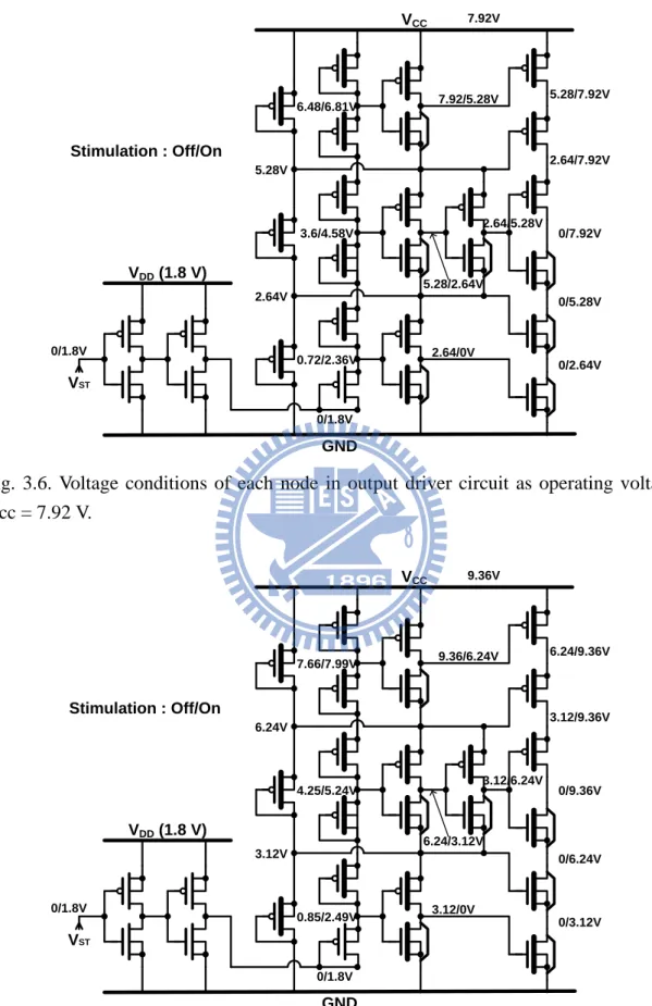
Fig. 3.6. Voltage conditions of each node in output driver circuit as operating voltage
Vcc = 7.92 V. 23
Fig. 3.7. Voltage conditions of each node in output driver circuit as operating voltage
Vcc = 9.36 V. 23
Fig. 3.8. The Vcc control circuit consisted of three comparators and logic gates. 24 Fig. 3.9. Structure of comparator in Vcc control circuit. 25
Fig. 3.10. K-map of control signals A and B derived from Table 3.1. 27 Fig. 3.11. The related logic gates of Eq. (3-1) and (3-2). 28
Fig. 3.12. The charge pump system. 29
29 Fig. 3.13 Reference voltage selector in the charge pump system. With selected r1 ~ r5,
the value of Vref depends on control signals A/B. 29
Fig. 3.14. Operating voltage of conventional design and that of proposed stimulus
driver verses tissue impedance. 31
Fig. 3.15. The simulation results of stimulus current and control signals as loading impedance RL = 250 kΩ and operating voltage Vcc = 5.04 V. 32
Fig. 3.16. The simulation results of stimulus current and control signals as loading impedance RL = 250 kΩ and operating voltage Vcc = 6.48 V. 33
Fig. 3.17. The simulation results of stimulus current and control signals as loading impedance RL = 250 kΩ and operating voltage Vcc = 7.92 V. 33
Fig. 3.18. The simulation results of stimulus current and control signals as loading impedance RL = 250 kΩ and operating voltage Vcc = 9.36 V. 34
Fig. 3.19. Simulation results of stimulus current as loading impedance RL = 100 kΩ
and 250 kΩ with their corresponding Vcc. 34
Fig. 3.20. Simulation results of stimulus current as loading impedance varying from
100 kΩ to 250 kΩ. 35
Fig. 3.21. Simulation results of operating voltage as loading impedance varying from
100 kΩ to 250 kΩ. 36
Fig. 3.22. Simulation results of power consumption as loading impedance varying
from 100 kΩ to 250 kΩ. 36
Fig. 3.23. (a) Layout and (b) chip photo of the proposed stimulus driver. 37 Fig. 3.24. Measurement setup of this work. Two Keithley 2400 source meters are used
to provide system supply voltage (VDD) and operating voltage (Vcc). HP
33120A function generator is utilized to provide the stimulation signal (VST). TDS 3054B is used to observe output voltage of the stimulus driver
and control signals A and B. 38
Fig. 3.25. The measurement results of stimulus current and control signals as loading impedance RL = 250 kΩ and operating voltage Vcc = 5.04 V. 39
Fig. 3.26. The measurement results of stimulus current and control signals as loading impedance RL = 250 kΩ and operating voltage Vcc = 6.48 V. 40
Fig. 3.27. The measurement results of stimulus current and control signals as loading impedance RL = 250 kΩ and operating voltage Vcc = 7.92 V. 40
Fig. 3.28. The measurement results of stimulus current and control signals as loading impedance RL = 250 kΩ and operating voltage Vcc = 9.36 V. 41
Fig. 3.29. Measurement results of stimulus current as loading impedance RL = 100 kΩ
and 250 kΩ with their corresponding Vcc. 41
Fig. 3.30. Measurement results of stimulus current as loading impedance varying from
100 kΩ to 250 kΩ. 42
Fig. 3.31. Measurement results of operating voltage as loading impedance varying
from 100 kΩ to 250 kΩ. 43
Fig. 3.32. Measurement results of power consumption as loading impedance varying
from 100 kΩ to 250 kΩ. 43
Fig. 3.33. Measurement setup of integration experiment of proposed stimulus driver and closed-loop epileptic seizure monitoring and controlling system. (a) Long-evans rats in this experiment, and (b) the proposed stimulus driver. 45 Fig. 3.34. The closed-loop epileptic seizure monitoring and controlling system utilized
in this animal test experiment. 45
Fig. 3.35. The waveform of stimulus current provided by the proposed stimulus driver
in this animal test experiment. 46
Fig. 3.36. The EEG of the Long-Evans rat under (a) normal condition and (b) epileptic
seizure in this animal test experiment. 47
Fig. 3.37. The procedure of normal condition, epileptic seizure, stimulus driver
activated, and epileptic seizure suppressed. 47
Fig. 4.1. Stimulus driver integrated with charge pump system. 51 Fig. 4.2. The waveform of voltage observed at the electrode while stimulating the
rat’s brain tissue with fixed stimulus current of 20 A (800 Hz, duty cycle =
40%). 52
Fig. 4.3. The waveform of voltage drop across a resistor (200 kΩ) while stimulus current of 20 A (800 Hz, duty cycle = 40%) flowing through it. 53 Fig. 4.4. Bi-phase stimulus driver with both positive and negative powers provides
biphasic stimulus current through one electrode per stimulus site. 54 Fig. 4.5. Bi-phase stimulus driver with only positive power provides biphasic current
between two electrodes per stimulus site. 54
Fig. 4.6. The method to implement biphasic stimulus current by making a copy of the output driver and placing it symmetrically to the origin circuit. 55
Chapter 1
Introduction
1.1 Motivation
As medical science and electronics engineering developed, new technologies combining medicine and microelectronics technology have been investigated and demonstrated. The applications of bioelectronics lead to a new generation of healthcare and therapies. There are several fabulous applications of bioelectronics such as magnetic resonance imaging and electroencephalography (EEG) that cause a revolution in medical science. In recent decades, it has been demonstrated that functional electrical stimulation (FES) and therapeutic electrical stimulation (TES) that transmit artificial electrical signals into nervous system can restore some physical functions of a human [1]. Hence the relationship between electrical transaction and nervous system has become indivisible. FES and TES have been studied for innovative medical treatments in different applications such as cardiac pacing, muscle exercising and even vision restoration [2]. Epilepsy is also one of diseases investigated to be treated by therapeutic electrical stimulation.
Epilepsy is the second most common neurological diseases, which is caused by transient abnormal discharge activity in brain. The incidence rates of epileptic seizures were found to be 1 % [3], which means there are tens of millions of people who suffer from epilepsy in the world. As medical science developed, some traditional therapies to cure epileptic seizure have been proposed such as pharmacologic treatment and surgical treatment. For a patient who suffers from epilepsy, pharmacologic treatment is the most
common used in the first place. However, some patients do not respond to the medicament, and there may be heavy side effects while taking pharmacologic treatment. For those conditions mentioned above, the surgical treatment is in common use. The non-reversible brain surgery is risky that might cause permanent functional losses. In addition, only 75% of patients do response well to the traditional therapies. Nowadays, epilepsy becomes predictable by analyzing EEG in time or frequency domains [4]. Several ways to predict epileptic seizure have been researched such as predictable features and prediction by classification. It has also been demonstrated that the abnormal discharge signal that causes epileptic seizure can be suppressed by TES before epilepsy happens [5]. To be compared with the non-reversible surgical treatment, the advantages of electrical stimulation treatment are flexible, recoverable, and non-destructive. It is more harmless to tissue in brain.
Though, TES is a feasible way to suppress epileptic seizure or cure other diseases, there are still several problems needed to be solved while providing the stimulus current for TES. Due to different kinds of tissue, locations, and implanted time, the equivalent impedance of electrode and tissue will vary in a wide range. The tissue impedance for individuals ranges from tens kΩ to hundreds kΩ. To provide fixed magnitude of stimulus current, the output voltage varies in a wide range corresponding to the tissue impedance. In addition, high operating voltage may result in problems of gate-oxide overstress, hot-carrier effect, and other reliability issues [6], [7], [8]. Furthermore, to an implantable device, power consumption is also an important consideration because it is inversely proportional to the use time. In this thesis, the proposed stimulus driver takes both reliability and power consumption into consideration. The stimulus driver with high-voltage-tolerant structure and the method of regulation of operating voltage to reduce power consumption are investigated and verified in this work.
1.2 Thesis Organization
The first chapter, chapter 1, includes the motivation of this work and the thesis organization.
The chapter 2 of this thesis introduces some background knowledge of epilepsy, epileptic seizure treatments, and design of implantable stimulus driver.
In the chapter 3, a new design of high-voltage-tolerant stimulus driver to suppress epileptic seizure with adaptive loading consideration is proposed. The integration of the proposed stimulus driver and closed-loop epileptic seizure monitoring and controlling system has been implemented and the function has been verified in the animal test experiment.
The last chapter, chapter 4, recapitulates the major consideration of this thesis and concludes with suggestions for future investigation.
Chapter 2
Background of Epilepsy, Effective Treatments
for Epilepsy, Epileptic Seizure Detecting and
Controlling System, and Design of Implantable
Stimulus Driver
2.1 Overview of Epilepsy
Epilepsy, the second most common neurological disease in the world, is caused by abnormal discharge of cells in brain. Brain to a human body is like a central process unit to a computer. It controls not only almost all the actions of a human but also sensations, emotions, memories, and so on. Signals between brain and different parts of body are delivered through the nervous system which consists of hundreds of thousands of neurons. Fig. 2.1 shows the nervous system in a human body which covers from head to toe [9]. Signals of actions from brain to organs are delivered by motor neurons, and signals of sensations from organs to brain are transmitted through sensory neurons. The way to pass a signal from one neuron to another is to excite it by chemical or electrical stimulation [10]. When a signal is going to be transmitted to the next neuron, some ions such as sodium, potassium, and chlorine are transferred through the ion channel to accumulate at the synapse as shown in Fig. 2.2(a). Accumulated ions cause the change of concentration of ions and voltage gradient of the membrane of neurons. If the voltage gradient exceeds the action potential to excite the neuron as shown in Fig. 2.2(b), the neuron will be triggered and the signal can be transmitted from the present neuron to the
next one. By a chain of this kind of electrical stimulations, signals can be transmitted between brain and different parts of human body.
Fig. 2.1. Nervous system in the human body [9].
(a) (b)
Fig. 2.2. The way neurons transmit signals is that (a) ions are transferred through membrane and accumulate at synapse to generate (b) action potential [10].
Under normal brain activity, brain generates constant and stable electrical signals in certain patterns. Fig. 2.3 shows different waveforms of EEG depending on states of body under normal conditions [11], [12]. These signals transmit along neurons of nervous system in the brain, spinal cord, and ganglia to whole body via neurotransmitters. During epileptic seizure time, abnormal discharges flow through nearby neurons and tissues. Like flowing through a resistor, current flows through nearby tissues will cause voltage drop. If the voltage exceeds the action potential, neurons will be triggered and unexpected signals will be spread out. In this case, normal activities of brain may be interrupted, and patients’ normal physical and emotional functions may be affected. Right side picture of Fig. 2.4 shows the EEG under abnormal brain activities recorded by the electrode array [13].
Due to the intensity of seizure, epilepsy can be roughly classified into two types: one is partial seizure, and the other is generalized seizure [14]. Partial seizure, which means abnormal discharge occurs just on one location of the brain, includes simple partial seizure and complex partial seizure. The difference between them is whether patients keep on conscious or unconscious during epileptic seizure time. When simple partial seizure occurs, patients remain conscious and can remember what happened during the seizure period. But, emotions, sensations, and motions are affected. Complex partial seizure has a greater influence on patients. During the seizure time, patients can not behave normally, control their motions, talk with other people, and so on. It is because patients usually become unconscious during complex partial seizure period, they won’t remember what happened after epileptic seizure.
According to different causes, syndromes, and locations of seizures, epilepsy can be classified into more than 40 types. Each type of epilepsy has unique seizure form, age group of patients, diagnosis, and treatment. Although most types of epileptic seizure won’t last a long time which may prolong only one or two minutes, epilepsy still affects
patients’ daily life deeply. Effective treatments to cure all the patients should be investigated.
Fig. 2.3. Brain activities under different states [11], [12].
Fig. 2.4. Left side picture is an electrode array that is used to record long-term brain activities of a patient. Right side picture is EEG of an epileptic patient, channels with black mark indicates that epileptic seizure occurs, channel with gray mark indicates nearby area that is affected by abnormal discharge which forms epileptic seizure [13].
2.2 Effective Treatments for Epilepsy
2.2.1 Available Epilepsy Treatment
Pharmacologic treatment is the most common way used to suppress epileptic seizure. Due to the diversification of epilepsy, there are more than 20 types of medications, and each is developed for specific type of epileptic seizure. According to patients’ age, types of epilepsy, syndromes, and intensity of seizure, doctors will choose suitable medications (antiepileptic drugs or AED) for treatment. There are two types of AEDs which can be used: one is narrow spectrum AEDs, and the other is broad spectrum AEDs. While the narrow spectrum AEDs focus on small number of epileptic seizure, the broad spectrum AEDs work for a large group of seizure. However, epilepsy is a complicated disease. There is no standard recipe to decide which medication is the best for an epileptic patient. Besides the effectiveness, side effects are also the mainly consideration for a doctor to write out a prescription. Most of patients’ condition of seizure can be ameliorated by AEDs. However, every kind of medicines might sometimes lead to side effects including blurry vision, dizziness, headaches, and fatigue [15]. In addition, these medications might lead to allergic in roughly 10 % of people and can impair blood cell or liver. Unfortunately, there are still many patients who do not respond to AEDs, which is called medically refractory. For these patients, other treatments should be taken into consideration such as surgical treatment.
Surgical treatment is an alternative for those medically refractory patients whose epileptic seizure cannot be controlled by medications [16]. Before the surgery, a cautious evaluation of the patient is taken. Through the evaluation, the brain location that abnormally discharges is located. Besides the brain areas, the functions which may be affected are found out as well. The evaluation includes long-term EEG recording, neurological examination, MRI, and so on. What kind of surgery is applied depends on
different kind of seizure and the location of the brain. There are two basic brain surgeries for epilepsy: one is resection surgery, and the other is disconnection surgery. In the resection surgery, the surgeon removes abnormal brain areas that initiate seizure. The most common type of resection surgery is temporal lobectomy. In disconnection surgery, which is sometimes called functional disconnection, the surgeon interrupts the nerve directions that spread abnormal discharges. Surgical treatment is not a suitable option for every patient whose seizure cannot be ameliorated by medications. Because some sections of brain are too important to be removed by the surgery. It is a risky treatment because patients may loss some physical functions permanently after taking the surgery. In addition, there is no guarantee that epileptic seizure can be cured completely by surgery.
Expect for traditional treatments such as pharmacologic treatment and surgical treatment mentioned above, electrical stimulation is an innovative treatment for drug-resistant epilepsy [17]. It has been investigated and approved currently. Advantages of electrical stimulation are flexible, recoverable, and non-destructive. Vagus nerve stimulation (VNS), is one kind of electrical treatment [18], [19]. The vagus nerve is autonomic nervous system, which controls physical functions that are not under voluntary control. The vagus nerve is situated the neck and connects abdomen and the lower part of brain. Device of VNS consists of pulse generator, flexible wires, and electrodes as shown in Fig. 2.5. By sending regular pulses of electrical signal via vagus nerve, VNS system can suppresses epileptic seizure before seizure happens. Currently, VNS is approved by Food and Drug Administration (FDA). Other electrical treatments have also been researched such as deep brain stimulation (DBS) shown in Fig. 2.6 [20], [21].
Fig. 2.5. Vagus nerve stimulation [18].
2.2.2 Epileptic Seizure Detecting and Controlling System
In recent decades, as bioelectronics developed, epileptic seizure becomes predictable by detecting and analyzing EEG in time or frequency domains [22], [23], [24]. Several methods to predict epileptic seizure such as predictable features, prediction by classification, and entropy calculation have been researched [25]. It has also been demonstrated that the abnormal discharge signal that causes epileptic seizure can be suppressed by TES before seizure happens. A variety of epileptic seizure detecting and controlling systems has been studied and implemented. The systems for epileptic treatment can be mainly classified into open-loop systems and closed-loop systems [26].
Open-loop systems, which are also called blind systems, are not able to respond to physiological activities immediately. The neuroscientists intend to modulate seizure by activating and inactivating regions and set the required stimulus current for individual region. Open-loop systems regularly turn on and off at a fixed pattern which is determined by neuroscientists before the event. Almost all of the currently existing systems that have been approved by FDA adopt open-loop systems [19]. Closed-loop systems, which are also called intelligent systems, are more complicated because they are able to respond to physiological activities immediately. The systems are switched on only when the physiological signals of epileptic seizure are detected. To be compared with open-loop systems, closed-loop systems can stimulate the location of seizure only and hence minimize the effect to human body. Closed-loop systems are consisted of detector, signal analyzer, controller, and stimulus driver.
As current researches shown, the seizure of epilepsy can be traced back to tens of seconds before onset by the EEG, which means that when the seizure-like brainwave is detected, there is still up to 10 seconds remained before the epileptic seizure happens [27]. During this time, the use of closed-loop systems may be effective to deal with
epileptic seizure. Therefore, a number of algorithms have been proposed for rapidly detecting and classifying the sign of different kinds of epileptic seizure. These algorithms analyze the brain activities recorded from EEG or electrocorticogram (ECoG) and extract the features of seizure-like brainwave, and the outcome of analysis can be utilized to decide whether to provide TES or not. Due to the complexity of closed-loop systems, power consumption is also one of mainly considerations while being applied to implantable systems. Fig. 2.7 shows a closed-loop epileptic seizure monitor and controller presented in 2011 [28].
Fig. 2.7. The closed-loop epileptic seizure monitor and controller system consisted of (a) microcontroller board, (b) signal conditioning board, and (c) stimulator board [28].
2.3 Brief Introduction of Implantable Stimulus Driver Technique
Therapeutic electrical stimulation (TES) and functional electrical stimulation (FES) have been developed and implemented for a variety of applications in medical science and clinical trials. In the past, some diseases were considered too difficult to be cured such as the retinitis pigmentosa (RP) [2], Alzheimer’s disease [29], and the damage of central nervous system. In the recent years, these diseases may become curable by TES. Thus a variety of implantable stimulus drivers have been researched and presented in order to provide stimulus current for TES. While designing implantable stimulus drivers,
there are many considerations that must be taken into account such as safety, reliability, voltage compliance, power consumption, charge balance, and density of stimulus sites. In this subsection, some previous works of stimulus drivers with different design considerations are briefly introduced. Both their advantages and disadvantages are mentioned as well.
Fig. 2.8 shows the stimulus driver with blocking-capacitor proposed in 2006 [30]. Some irresistible factors may cause the damage of implanted devices such as moisture. A failure in output stage of implanted device may lead to prolonged dc current flowing from stimulus driver to human body and result in serious damage. For the consideration of safety, the use of off-chip blocking-capacitor in output stage of stimulus drivers is adopted. By the use of blocking-capacitor, the prolonged dc current flowing from stimulus driver to human body can be prevented. However, the size of capacitors is too large, and capacitors usually dominate the size of implantable stimulus driver.
To improve the disadvantage mentioned above, the technique pronounced in 2006 utilized two complementary current sources to deliver stimulus current [30]. By delivering stimulus current through one capacitor and discharging accumulated charge on the other capacitor, the purpose to deliver complementary stimulus current is achieved. In this way, the size of blocking-capacitor is reduced by the ratio of switching rate of the two current sources. Thus, reduced capacitors can be integrated into implantable stimulus driver. Despite the disadvantage of large size can be improved, there are still problems while using blocking-capacitors. The blocking-capacitors provide output stage of stimulus driver with extra voltage drop, so the required operating voltage of the circuit is higher. It directly decreases voltage compliance of the circuit.
The stimulus driver delivers stimulus current through electrodes into the tissue. While stimulus current is conducted, chemical process may occur at the electrode-tissue
interface. Some studies revealed that unbalanced stimulus current may cause net charge to store in body and lead to destructive problems such as electrolysis, gazing, pH changing, and dissolution [31], [32]. In order to solve these problems, some bi-phase stimulus drivers have been presented. The purpose of these works is to generate balanced current of anodic pulse and cathodic pulse [33].
There are many other considerations while designing implantable stimulus driver. In order to provide constant stimulus current irrespective of high variety of loading impedance, stimulus driver of high output impedance should be considered. Fig. 2.9 [33] shows the improved current sources with fully cascaded structure which provides high impedance at the output. Another stimulus driver with voltage controlled resisters (VCR) current source shown in Fig. 2.10 [34] utilizes MOS transistors operating in deep triode region to gain the voltage compliance close to the fixed power supply. Indeed, while designing a stimulus driver, it is rare that just one of the considerations is taken into account [35]. This work investigates stimulus driver for epileptic seizure control with considerations of reliability, safety, variation of tissue impedance, and power consumption.
A
C
Nerve
IstimA
IstimC
Blocking
Capacitor
S1
S2
S3
VDD
VSS
Fig. 2.8. Stimulator output stage with blocking capacitor [30].
DA C Digi ta l In puts Tissue Site Site VCC VCC VBIAS I OUT
00 01 02 03 04 DA C Digi ta l In puts + -+ -Tissue Site Site I OUT VCC Vsink Vin
Chapter 3
Design of High-Voltage-Tolerant Stimulus Driver
to Suppress Epileptic Seizure with Adaptive
Loading Consideration in 0.18-μm CMOS
Process
3.1 Introduction
Epilepsy is one of the most common neurological disorder that caused by abnormal discharge in brain. Traditional therapies include pharmacologic treatment and surgical treatment. Pharmacologic treatment is the most common used. For patients who do not respond to the medicament, non-reversible brain surgery is in common use. But the risky surgery may cause functional loss. Furthermore, only 75% do response to traditional therapies [5]. In recent years, functional electrical stimulation (FES) and therapeutic electrical stimulation (TES) have been demonstrated that can restore some physical functions of a human. Epilepsy is also one of diseases investigated to be treated by therapeutic electrical stimulation. Nowadays, epileptic seizure becomes predictable by detecting premonition of epileptic seizure from electroencephalography (EEG) or electrocorticogram (ECoG) in time or frequency domains. It has been demonstrated that the epileptic seizure caused by abnormal discharge signals can be suppressed by electrical stimulation before seizure happens. Compare to non-reversible surgical treatment, the advantages of electrical stimulation therapies are harmless to the tissue of the brain. Besides, it can make adjustment arbitrarily and is more flexible. As the
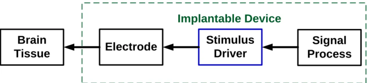
transistor size reduces in CMOS technology, devices can integrates into a chip that is implantable. Fig. 3.1 shows the block diagram of an implantable stimulus driver system for epileptic treatment.
Signal Process Stimulus Driver Electrode Brain Tissue Implantable Device
Fig. 3.1. The block diagram of an implantable stimulus driver for epilepsy treatment.
Due to different kinds of tissue, locations, and implanted time, the equivalent impedance of electrode and tissue will vary in a wide range. The tissue impedance for individuals ranges from tens kΩ to hundreds kΩ [28]. According to the specifications derived from experimental demand, the range of stimulus current, which is able to suppress epileptic seizures without being harmful to the rats, is within 35 μA to 50 μA. The output current of this proposed stimulus driver is then set to fit the specification. The equivalent tissue impedance is within 100 kΩ to 250kΩ. By multiplying tissue impedance by stimulus current, high voltage (~10 V) occurs at the output of stimulus driver. To prevent reliability issues, using some special structures to sustain the high voltage is needed [36] – [40]. To an implantable device, power consumption is also an important consideration. With the considerations of reliability, safety, and power consumption, the stimulus driver used in the implantable device for seizure control is investigated in this work. The detailed circuit simulation and measurement results of the proposed design will be presented in the following sections.
3.2 Novel High-Voltage-Tolerant Stimulus Driver with Adaptive
Loading Consideration Fabricated in 0.18-μm CMOS Process
3.2.1 Implementation
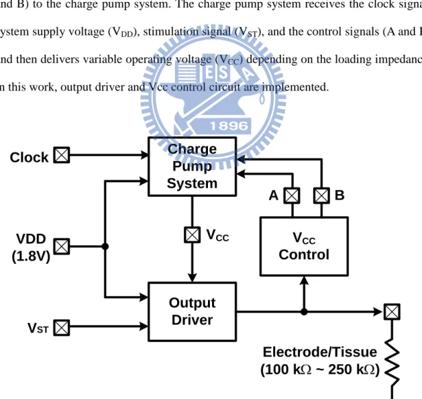
Fig. 3.2 shows the block diagram of proposed stimulus driver, which contains charge pump system, output driver, and Vcc control circuit. The output driver receives the system supply voltage (VDD), stimulation signal (VST), and variable operating
voltage (VCC), and then delivers the stimulus current to the load (electrode/tissue). The
VCC control circuit detects the stimulus current, and then sends the control signals (A
and B) to the charge pump system. The charge pump system receives the clock signal, system supply voltage (VDD), stimulation signal (VST), and the control signals (A and B),
and then delivers variable operating voltage (VCC) depending on the loading impedance.
In this work, output driver and Vcc control circuit are implemented.
Charge
Pump
System
Output
Driver
V
CCControl
Electrode/Tissue
(100 k
W
~ 250 k
W
)
V
CCA
VDD
(1.8V)
V
STB
Clock
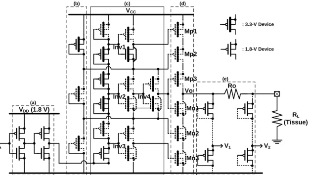
VCC GND RL (Tissue) V2 V1 Ro VDD (1.8 V) Mp1 Vo Mp2 Mp3 Mn3 Mn2 Mn1 Inv1 Inv2 Inv3 Inv4 (a) (b) (c) (d) (e) : 3.3-V Device : 1.8-V Device
Fig. 3.3. Structure of output driver fabricated in 0.18-μm 1.8-V/3.3-V CMOS process. 3.3-V transistors are shown with thick gate oxide, and 1.8-V transistors are shown with thin gate oxide.
The output driver circuit fabricated in 0.18-μm CMOS process is shown in Fig. 3.3. Both 3.3-V transistors (shown with thick gate oxide) and 1.8-V transistors (shown with thin gate oxide) are used. In order to sustain the high voltage (~10V) without gate-oxide overstress, the stacked MOS configuration with 3.3-V transistors between Vcc and ground is used. The output driver can be divided into five parts: input buffer, bias circuit, control circuit, output stage, and detection circuit. The input buffer is used to provide a full-swing of 1.8 V while receiving the stimulation signal (VST). The bias circuit, which
consists of three PMOS diodes, is used to provide the biases of 2Vcc/3 and Vcc/3. The control circuit, which is made up of a PMOS-diode chain and four inverters, plays the role of a level shifter. When VST is high, the voltage at the bottom of the PMOS-diode
chain is 1.8 V. Through the PMOS-diode chain, all the input voltages of the three inverters Inv1, Inv2, and Inv3 equal to logic “1,” and the input voltage of Inv4 equals to logic “0.” In this condition, the output voltages of Inv1, Inv4, and Inv3 are 2Vcc/3, 2Vcc/3, and 0 V, respectively. The gate voltages of Mp1, Mp2, Mp3, Mn1, Mn2, and
Mn3 are 2Vcc/3, 2Vcc/3, 2Vcc/3, 2Vcc/3, Vcc/3, and 0 V, respectively. Mp1, Mp2, and Mp3 are turned on to transfer stimulus current, and all the drain voltages of them almost equal to Vcc. Mn1, Mn2, and Mn3 are turned off, and drain voltages of them are Vcc, 2Vcc/3, and Vcc/3, respectively. When VST is low, the voltage at the bottom of the
PMOS-diode chain is 0 V. Through the PMOS-diode chain, all the input voltages of the three inverters Inv1, Inv2, and Inv3 equal to logic “0,” and the input voltage of Inv4 equals to logic “1.” In this condition, the output voltages of Inv1, Inv4, and Inv3 are Vcc, Vcc/3, and Vcc/3, respectively. The gate voltages of Mp1, Mp2, Mp3, Mn1, Mn2, and Mn3 are Vcc, 2Vcc/3, Vcc/3, Vcc/3, Vcc/3, and Vcc/3, respectively. Mn1, Mn2, and Mn3 are turned on to discharge the output node Vo, and all the drain voltages of them equal to 0 V. Mp1, Mp2, and Mp3 are turned off, and drain voltages of them are 2Vcc/3, Vcc/3, and 0 V, respectively. For both the cases VST is high or low, the max
voltage of |VGS|, |VDS|, and |VGD| is Vcc/3. The max voltage drop across a 3.3-V device
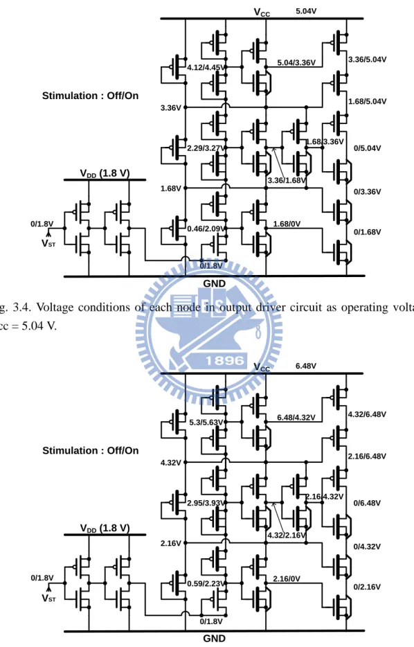
is 3.12V because the max operating voltage Vcc here we use is 9.36 V. So there is no gate-oxide overstress happened. Fig. 3.4 to Fig. 3.7 show the voltage conditions of each node of the output driver in four different operating regions of Vcc = 5.04 V, 6.48 V, 7.92 V, and 9.36 V, respectively. The stimulation is controlled by the 1.8-V signal (VST).
Whether the stimulation is turned off or on, all voltage differences across the MOS transistors are lower than their sustainable voltages (1.8 V or 3.3 V) to prevent reliability issues. The detection circuit is consisted of two PMOS-diode chains and one output resistor. The output resistor (RO = 2 kΩ) is arranged before the electrode and the
tissue. When the stimulus current flows through Ro, a voltage drop across Ro occurs. Two PMOS-diode chains connected to each end of Ro are used to generate biases V1 and V2. As the value of V1 lies in the value of Vcc, the value of V2 lies in both the value of Vcc and the stimulus current (Istim). The voltage difference between V1 and V2
VCC GND VDD (1.8 V) 5.04V 3.36/5.04V 1.68/5.04V 0/5.04V 0/3.36V 0/1.68V 3.36V 1.68V 0/1.8V VST 5.04/3.36V 1.68/3.36V 3.36/1.68V 1.68/0V 0.46/2.09V 2.29/3.27V 4.12/4.45V Stimulation : Off/On 0/1.8V
Fig. 3.4. Voltage conditions of each node in output driver circuit as operating voltage Vcc = 5.04 V. VCC GND VDD (1.8 V) 6.48V 4.32/6.48V 2.16/6.48V 0/6.48V 0/4.32V 0/2.16V 4.32V 2.16V 0/1.8V VST 6.48/4.32V 2.16/4.32V 4.32/2.16V 2.16/0V 0.59/2.23V 2.95/3.93V 5.3/5.63V Stimulation : Off/On 0/1.8V
Fig. 3.5. Voltage conditions of each node in output driver circuit as operating voltage Vcc = 6.48 V.
VCC GND VDD (1.8 V) 7.92V 5.28/7.92V 2.64/7.92V 0/7.92V 0/5.28V 0/2.64V 5.28V 2.64V 0/1.8V VST 7.92/5.28V 2.64/5.28V 5.28/2.64V 2.64/0V 0.72/2.36V 3.6/4.58V 6.48/6.81V Stimulation : Off/On 0/1.8V
Fig. 3.6. Voltage conditions of each node in output driver circuit as operating voltage Vcc = 7.92 V. VCC GND VDD (1.8 V) 9.36V 6.24/9.36V 3.12/9.36V 0/9.36V 0/6.24V 0/3.12V 6.24V 3.12V 0/1.8V VST 9.36/6.24V 3.12/6.24V 6.24/3.12V 3.12/0V 0.85/2.49V 4.25/5.24V 7.66/7.99V Stimulation : Off/On 0/1.8V
Fig. 3.7. Voltage conditions of each node in output driver circuit as operating voltage Vcc = 9.36 V.
The purpose of Vcc control circuit is to generate control signals, so the charge pump system can generate a corresponding value of operating voltage Vcc according to the present control signals. In this work, we desire to generate four levels of Vcc (5.04, 6.48, 7.92, and 9.36 V), so control signals of two bits A/B are required. The Vcc control circuit consists of three comparators (C1, C2, and C3) and logic gates circuit as shown in Fig. 3.8. Here we transfer V1 and V2, which are derived from detection circuit of output driver, to the inputs of these three comparators. Fig. 3.9 shows the structure of the comparators, each of them consists of a differential pair (M1 and M2), a current mirror (M3 and M4), a resistor (Rs), a current source (M5), and an inverter (M6 and M7). + - + - +
-C1
C2
C3
Logic Gates
A
B
V1 V2 X Y ZV1
V2
V
bias
X,Y,Z
Rs
M3
M4
M2
M1
M5
Mp
Mn
GND
V
DDFig. 3.9. Structure of comparator in Vcc control circuit.
If the voltage difference between V1 and V2 is not large enough, VGS of M1 will
be smaller than that of M2 due to the voltage drop across Rs. This causes the current flowing through M3 to be smaller than that of M4, so the drain voltage of M4 tends to be a low level (logic “0”), and the output of the inverter is raised to a high level (logic “1”). On the other hand, the output of the comparator will be a low level (logic “0”) if the voltage difference between V1 and V2 is large enough. To design the Vcc control circuit, we can consider the impedance of the electrode and tissue (RL) changing
gradually from the minimum (100 kΩ) to the maximum (250 kΩ). At the beginning, RL
= 100 kΩ and Vcc = 5.04 V, the current flowing through Ro (~Istim) is large, so the
differential voltage between V1 and V2 is large enough. This causes the output of the comparator to be logic “0.” As RL increases, Istim and differential voltage between V1
specification. At this operating point (here we choose RL = 130 kΩ), Vcc should be
changed to a higher level in order to provide enough stimulus current. By selecting a proper value of Rs, we can make the output of comparator C1 change from logic “0” to “1” when the loading impedance reaches the value RL = 130 kΩ. Consider that when
Vcc changes from 5.04 V to 6.48 V due to the output of C1 changing from “0” to “1,” the stimulus current is raised as well. Raised Istim through Ro makes the voltage
difference between V1 and V2 become larger. If the current flowing through Rs can’t be enlarged simultaneously, the output of C1 will change back to “0,” and then will vary between “0” and “1” repeatedly. In order to avoid this unstable condition, it is necessary to enlarge the current through Rs when Vcc changes to a high level. We notice that not only the differential voltage between V1 and V2 rises with increased Vcc, but also the common-mode voltage does. There are two ways to enlarge the current through Rs as the common-mode voltage is raised: one is to replace M5 by a resistor, and the other is to operate M5 in triode region at the beginning. The second method is adopted here because it occupies less layout area and consumes less power than the first method. The reason why it consumes less power is that when Vcc changes to a higher level again (from 6.48 V to 7.92 V), by using a resistor to replace M5 as the current source, the current flowing through the current source will rise again. If M5 is designed to turn from triode region into saturation region at the first time Vcc increases, then the current through M5 won’t rise obviously at the second time Vcc increases. Hence it has less power consumption than using a resistor. As the comparator C1 is designed to change Vcc from 5.04 V to 6.48 V, C2 and C3 are designed to change Vcc from 6.48 V to 7.92 V and from 7.92 V to 9.36 V, and each M5 of them turns from triode region into saturation region in the meantime Vcc changes. The corresponding operating points to change Vcc from 6.48 V to 7.92 V and from 7.92 V to 9.36 V are RL = 170 kΩ and RL =
comparators X/Y/Z, desired control signals A/B, and corresponding Vcc. According to Table 3.1, The K-map shown in Fig. 3.10 can be drawn. The logic gates circuit to generate control signals A/B can be accomplished by deriving Eq. (3-1) and (3-2) from the K-map.
.
A = Y (3-1) B = XZ’ (3-2)
The logic gates circuit corresponding to Eq. (3-1) and (3-2) are shown in Fig. 3.11.
Table 3.1. Relationship of V1, V2, comparator outputs, control signals, operating voltage, and reference voltage.
X YZ 0 1 0 0 0 1 1 1 1 0 1 1 0 0 X X X X X YZ 0 1 0 0 0 1 1 1 1 0 1 1 0 0 X X X X
A:
B:
X
Z’
B
Y
A
Fig. 3.11. The related logic gates of Eq. (3-1) and (3-2).
The Vcc control circuit behaves like a state machine to send out control signals A/B as 0/0→0/1→1/1→1/0 with corresponding outputs of comparators X/Y/Z as 0/0/0→1/0/0→1/1/0→1/1/1. At the beginning of the stimulation condition, X/Y/Z are 0/0/0, A/B are 0/0, and 5.04-V Vcc is delivered to the output driver initially. If the loading impedance (RL) is within 100 kΩ to 130 kΩ, X/Y/Z, A/B, and Vcc keep their
origin values. If the loading impedance is higher than 130 kΩ, 170 kΩ, and 210 kΩ, the A/B signals become 0/1, 1/1, and 1/0, respectively with corresponding comparators outputs 1/0/0, 1/1/0, and 1/1/1. In the mean time, 6.48-V, 7.92-V, and 9.36-V Vcc are delivered to the output driver. After the stimulation condition, the stimulus driver is turned off, and control signals A/B are reset to 0/0.
The charge pump system is shown in Fig. 3.12 [41], which contains a reference voltage selector (Vref selector) shown in Fig. 3.13. From Table 3.1, the ratio of resistors
in the Vref selector can be derived as shown in Eq. (3-3), and the output voltage of the
Vref selector (Vref) equals 7VDD/15 (0.84V), 9VDD/15 (1.08V), 11VDD/15 (1.32V), or
13VDD/15 (1.56V), according to the control signals A/B = 0/0, 0/1, 1/1, 1/0,
respectively .
Charge Pump Circuit VDD Clock Generator Clkr Vref + -5R R Vcc CL 100 A
Fig. 3.12. The charge pump system.
A A B B VDD Vref r1 r2 r3 r4 r5
Fig. 3.13 Reference voltage selector in the charge pump system. With selected r1 ~ r5, the value of Vref depends on control signals A and B.
Once the control signals are decided, the corresponding Vref is delivered to the
comparator (V+) shown in Fig. 3.12. The other input of the comparator (V-) is Vcc/6. If Vcc/6 is smaller than Vref, the output of comparator is “1,” the clock generator activates
charge pump circuit and Vcc increases. When Vcc/6 becomes slightly larger than Vref,
the charge pump circuit keeps delivering steady VCC by means of the feedback loop in
the charge pump system. Fig. 3.14 shows the operating voltage Vcc of proposed stimulus driver verses tissue impedance. Operating voltage of conventional design is also contained in Fig. 3.14 to be compared. The proposed stimulus driver operates at four different levels of Vcc in accordance of loading impedance while conventional works operating with fixed operating voltage. For the condition of fixed stimulus current and low loading impedance, this work with lower operating voltage is more power efficient than conventional ones, and hence has less power consumption.
In this work, only output driver and Vcc control circuit are implemented. The charge pump system is not contained.
80 100 120 140 160 180 200 220 240 260 3 4 5 6 7 8 9 10 R e q u ir e d O p e ra ti n g V o lt a g e ( V ) Tissue Impedance (kW)
Required Operating Voltage This Work
Conventional Works
Fig. 3.14. Operating voltage of conventional design and that of proposed stimulus driver verses tissue impedance.
3.2.2 Simulation Results
Fig. 3.15 to Fig. 3.18 show how to decide the correct level of Vcc with corresponding tissue impedance by simulation results while simulating, and the upper limit tissue impedance of this design (RL = 250 kΩ) is adopted here. At the beginning,
Vcc is set to be 5.04 V originally, stimulus current Istim = 19.69 μA, and control signals
A/B = 0/1 as shown in Fig. 3.15. With corresponding to A/B = 0/1, Vcc should be set to 6.48 V, and then repeat the simulation. The simulation results for Vcc = 6.48 V are Istim
= 25.42 μA, and control signals A/B = 1/1 as shown in Fig. 3.16. With corresponding to A/B = 1/1, Vcc should be change to 7.92 V, and then repeat the simulation. The simulation results for Vcc = 7.92 V are Istim = 31.12 μA, and control signals A/B = 1/0
as shown in Fig. 3.17. Simulation should be repeat again with Vcc = 9.36 V since A/B = 1/0. The simulation results for Vcc = 9.36 V are Istim = 36.82 μA, and control signals
A/B = 1/0 as shown in Fig. 3.18. From the simulation results, the control signals A/B maintain the same values as that of Vcc = 7.92 V, which means the present value of Vcc is suitable for RL = 250 kΩ, and the stimulus current with sufficient magnitude is
provided by the stimulus driver. The simulation results of stimulus current as loading impedance RL = 100 kΩ and 250 kΩ with their corresponding Vcc are shown in Fig.
3.19.
Fig. 3.15. The simulation results of stimulus current and control signals as loading impedance RL = 250 kΩ and operating voltage Vcc = 5.04 V.
Fig. 3.16. The simulation results of stimulus current and control signals as loading impedance RL = 250 kΩ and operating voltage Vcc = 6.48 V.
Fig. 3.17. The simulation results of stimulus current and control signals as loading impedance RL = 250 kΩ and operating voltage Vcc = 7.92 V.
(d)
Fig. 3.18. The simulation results of stimulus current and control signals as loading impedance RL = 250 kΩ and operating voltage Vcc = 9.36 V.
0.0 0.5 1.0 1.5 2.0 0 10 20 30 40 50 60 S ti m u la ti o n C u r r e n t ( A) Time (ms) 100kW 250kW
Fig. 3.19. Simulation results of stimulus current as loading impedance RL = 100 kΩ and
In this work, tissue impedance is classified into 4 groups as 100 kΩ ~ 130 kΩ, 130 kΩ ~ 170 kΩ, 170 kΩ ~ 210 kΩ, and 210 kΩ ~ 250 kΩ. To satisfy the proposed current range, each group of tissue impedance is designed to provide operating voltage Vcc = 5.04 V, 6.48 V, 7.92 V, and 9.36 V, respectively. The simulation results of stimulus current, operating voltage Vcc, and power consumption as loading impedance changing from RL = 100 kΩ to RL = 250 kΩ are shown in Fig. 3.20, Fig. 3.21, and Fig. 3.22,
respectively. It is obvious that simulation result of power consumption looks like a four-level steps because the four different levels of Vcc are in use.
The proposed high-voltage-tolerant stimulus driver to suppress epileptic seizure with adaptive loading consideration has been fabricated in TSMC 0.18-μm 1.8-V/3.3-V CMOS process. Fig. 3.23 shows the layout and chip photo of the proposed stimulus driver. The chip size of the stimulus driver is 500 340 m2.
100 150 200 250 0 10 20 30 40 50 60 25oC 100oC S ti m u la ti o n C u r r e n t ( A) Loading Impedance (kW)
Fig. 3.20. Simulation results of stimulus current as loading impedance varying from 100 kΩ to 250 kΩ.
100 150 200 250 0 2 4 6 8 10 O p e r a ti n g V o lt a g e ( V ) Loading Impedance (kW)
Fig. 3.21. Simulation results of operating voltage as loading impedance varying from 100 kΩ to 250 kΩ. 100 150 200 250 0.0 0.2 0.4 0.6 0.8 1.0 P o w e r C o n su m p ti o n ( m W ) Loading Impedance (kW)
Fig. 3.22. Simulation results of power consumption as loading impedance varying from 100 kΩ to 250 kΩ.
(a)
(b)
Fig. 3.23. (a) Layout and (b) chip photo of the proposed stimulus driver.
3.2.3 Measurement Results
The measurement setup of proposed design is shown in Fig. 3.24, where two Keithley 2400 source meters, one Hp 33120A function generator, and one TDS 3054B
oscilloscope are in use. One Keithley 2400 is utilized to provide the prototype of proposed design with system supply voltage (VDD) of 1.8 V, and the other is utilized to
replace the charge pump system to provide variable operating voltage Vcc according to observed control signals A/B. Hp 33120A is utilized to provide the stimulation signal (VST) to enable stimulus driver. TDS 3054B is used to observe output voltage of the
stimulus driver and control signals A/B. By dividing the output voltage by the loading impedance, the magnitude of stimulus current can be obtained.
Fig. 3.24. Measurement setup of this work. Two Keithley 2400 source meters are used to provide system supply voltage (VDD) and operating voltage (Vcc). HP 33120A
function generator is utilized to provide the stimulation signal (VST). TDS 3054B is used
to observe output voltage of the stimulus driver and control signals A and B.
To verify the performance of proposed stimulus driver, the process which we use to decide the correct Vcc with corresponding RL while doing simulation is taken. Also, the
Vcc is set to be 5.04 V originally, the observed stimulus current Istim = 19.2 A, and
control signals A/B = 0/1 as shown in Fig. 3.25. With corresponding to A/B = 0/1, Vcc should be set to 6.48 V, and then repeat the measurement. The measurement results for Vcc = 6.48 V are Istim = 24.96 A, and control signals A/B = 1/1 as shown in Fig. 3.26.
With corresponding to A/B = 1/1, Vcc should be change to 7.92 V, and then repeat the measurement. The measurement results for Vcc = 7.92 V are Istim = 31.36 A, and
control signals A/B = 1/0 as shown in Fig. 3.27. Measurement should be repeat again with Vcc = 9.36 V since A/B = 1/0. The measurement results for Vcc = 9.36 V are Istim =
37.2 A, and control signals A/B = 1/0 as shown in Fig. 3.28. According to the above measurement procedure, the function to generate correct control signals A and B is verified. The measurements results as loading impedance RL = 100 kΩ and 250 kΩ with
their corresponding Vcc are shown in Fig. 3.29.
Fig. 3.25. The measurement results of stimulus current and control signals as loading impedance RL = 250 kΩ and operating voltage Vcc = 5.04 V.
Fig. 3.26. The measurement results of stimulus current and control signals as loading impedance RL = 250 kΩ and operating voltage Vcc = 6.48 V.
Fig. 3.27. The measurement results of stimulus current and control signals as loading impedance RL = 250 kΩ and operating voltage Vcc = 7.92 V.
Fig. 3.28. The measurement results of stimulus current and control signals as loading impedance RL = 250 kΩ and operating voltage Vcc = 9.36 V.
0.0 0.5 1.0 1.5 2.0 0 10 20 30 40 50 60 S ti m u la ti o n C u rr e n t ( A) Time (ms) 100k 250k
Fig. 3.29. Measurement results of stimulus current as loading impedance RL = 100 kΩ
Fig. 3.30 shows the measurement result of stimulus current as loading impedance changing from RL = 100 kΩ to RL = 250 kΩ. The measurement result shows that
loading impedance is classified into 4 groups as 100 kΩ ~ 133 kΩ, 133 kΩ ~ 168 kΩ, 168 kΩ ~ 213 kΩ, and 213 kΩ ~ 250 kΩ. The result is close to our design which we classify loading impedance into 4 groups as 100 kΩ ~ 130 kΩ, 130 kΩ ~ 170 kΩ, 170 kΩ ~ 210 kΩ, and 210 kΩ ~ 250 kΩ originally. The stimulus current is in the range of 36.98 A ~ 49.6 A, which fits in the range of 35 A ~ 50 A. The measurement results of operating Vcc and power consumption are shown in Fig. 3.31 and Fig. 3.32. The power consumption is within 0.24 mW to 0.87 mW.
100 150 200 250 0 10 20 30 40 50 60 S ti m u la ti o n C u rr e n t ( A) Loading Impedance (kW) Measurement Simulation
Fig. 3.30. Measurement results of stimulus current as loading impedance varying from 100 kΩ to 250 kΩ.
100 150 200 250 0 2 4 6 8 10 O p e r a ti n g V o lt a g e ( V ) Loading Impedance (kW)
Fig. 3.31. Measurement results of operating voltage as loading impedance varying from 100 kΩ to 250 kΩ. 100 150 200 250 0.2 0.3 0.4 0.5 0.6 0.7 0.8 0.9 1.0 P o w e r C o n s u m p ti o n ( m W ) Loading Impedance (kW) Measurement Simulation
Fig. 3.32. Measurement results of power consumption as loading impedance varying from 100 kΩ to 250 kΩ.
3.2.4 Integration of the Proposed Stimulus Driver and Epileptic Seizure Monitoring
and Controlling System
The animal test experiment is conducted by Neural Computing and Brain Computer Interface Lab of National Cheng-Kung University. In this experiment, the stimulus driver has been integrated into the closed-loop epileptic seizure monitoring and controlling system. Long-evens rats, born with spontaneous absence epileptic seizure, are selected for experiment in this study. The rats of aged 4 - 6 months and weighting 500 - 700 g were anesthetized with sodium pentobarbital (50 mg/kg, i.p.). All surgical and experimental procedures were reviewed and approved by Institutional Animal Care and Use Committee of National Cheng-Kung University.
The closed-loop epileptic seizure monitoring and controlling system consists of data acquisition (EEG detection), wireless transceiver, host computer (signal process), microcontroller (stimulator activation). By analyzing brain activities of Long-evans rats which suffer from spontaneous absence seizure and epileptiform activities induced by pentylenetetrazol (PTZ), the system can detects epileptic seizure simultaneously and stimulates the right-side zona incerta (ZI) (posterior 4.0 mm, lateral 2.5 mm, and depth 6.7-7.2 mm). Stimulus current is conducted by a 4-microwire bundle, each made of Teflon-insulted stainless steel wire while ground electrode was implanted 2 mm caudal to lambda.
Fig. 3.33 shows the measurement setup of integration experiment of proposed stimulus driver and closed-loop epileptic seizure monitoring and controlling system. An additional computer is used to receive and process the EEG signals to decide whether epileptic seizure happens or not, and then sends the control signals back. The chips utilized to detect brain activities of Long-evans rats, send EEG signals to the computer, and receive control signals from the computer to activate the stimulus driver on the rat’s head are shown in Fig. 3.34.
![Fig. 2.1. Nervous system in the human body [9].](https://thumb-ap.123doks.com/thumbv2/9libinfo/8343733.176149/18.892.140.716.218.1075/fig-nervous-human-body.webp)
![Fig. 2.5. Vagus nerve stimulation [18].](https://thumb-ap.123doks.com/thumbv2/9libinfo/8343733.176149/23.892.156.679.123.1109/fig-vagus-nerve-stimulation.webp)
![Fig. 2.7. The closed-loop epileptic seizure monitor and controller system consisted of (a) microcontroller board, (b) signal conditioning board, and (c) stimulator board [28]](https://thumb-ap.123doks.com/thumbv2/9libinfo/8343733.176149/25.892.191.710.482.660/epileptic-seizure-monitor-controller-consisted-microcontroller-conditioning-stimulator.webp)
![Fig. 2.10. Voltage controlled resistor current source of stimulator [34].](https://thumb-ap.123doks.com/thumbv2/9libinfo/8343733.176149/29.892.177.647.134.769/fig-voltage-controlled-resistor-current-source-stimulator.webp)