國 立 交 通 大 學
光 電 工 程 學 系 碩 士 班
碩 士 論 文
利用新穎材料提升氮化鎵太陽能電池的效率
Enhanced Power Conversion Efficiency of GaN-Based Solar Cell
by Novel Materials
研究生:曹庭耀
.指導教授:郭浩中教授
謝嘉民教授
利用新穎材料提升氮化鎵太陽能電池的效率
Enhanced Power Conversion Efficiency of GaN-Based Solar Cell by
Novel Materials
研究生:曹庭耀 Student:Ting-Yao Tsao
指導教授:郭浩中 教授 Advisor:Hao-Chung Kuo
謝嘉民 教授 Jia-Min Shieh
國 立 交 通 大 學
光 電 工 程 學 系 碩 士 班
碩 士 論 文
A Thesis
Submitted to Photonics Institute
College of Electrical Engineering
National Chiao Tung University
in Partial Fulfillment of the Requirements
for the Degree of
Master
In
Photonics
July 2012
Hsinchu, Taiwan, Republic of China
i
利用新穎材料提升氮化鎵太陽能電池的效率
研究生:曹庭耀 指導教授:郭浩中 教授
謝嘉民 教授
國立交通大學光電工程學系碩士班
摘要
在本論文中,我們針對氮化鎵太陽能電池的反射率高於 20%而導致效率不佳的問題 來做一個改良,另一部份是針對氮化鎵太陽能電池短波段的入射光被表面的透明導電層 所吸收而導致短波段光都浪費掉的問題來做一個改善,主要是針對這兩個問題而改進進 而提升我們氮化鎵太陽能電池的效率。 本論文第一部分是在討論如何改善反射率高的問題,很多文獻顯示,我們如果在表 面製作奈米結構可以達到降低反射率的效果。所以我們製作具有奈米結構的 PDMS 模, 這種模製程可以大面積而且便宜方便,不需要像其他做奈米結構要在真空下面進行,而 且我們發現這樣製作出來的 PDMS 模具有很好的抗反射的效果,而且不只這樣,這種模 也具有讓光散射的效果,讓光在電池裡行徑路徑比較長,有利增加我們效率。之後,我 們將此種具有降低反射效果的 PDMS 模應用在我們氮化鎵太陽能電池上,並針對元件之 反射率、外部量子效應、光電轉換效率等來進行分析,並以變角度反射率量測來證明次 波長結構在變角度下仍然有不錯的抗反射效果,因此我們觀察到全波段量子效率的提升, 將此具有 PDMS 模的電池相較於沒有 PDMS 模的電池,提高了 7.2%光電流增加與光電轉換 效率 7.1%的增強,有效驗證了 PDMS 模對於氮化鎵太陽能電池光電轉換效率之提昇是有 幫助的。 本論文第二部分是在針對氮化鎵太陽能電池短波段的入射光被表面的透明導電層ii 所吸收而導致短波段光都浪費掉的問題來做一個改善。因為短波長紫外光區域具有全太 陽頻譜 7%,如果我們可以好好利用這些光會對我們效率有很大的幫助。 所以我用了量子點(quantum dot),我們選用 400nm 的 CdS 量子點,這種量子點會 吸收在 400 以前的光進而再放射出 400nm 左右的可見光,可以被我們氮化鎵太陽能電池 所吸收利用,我們是在做好的元件上面點上我們的量子點讓它在表面是一層膜,他就可 以在 ITO 吸收短波長之前吸收我們的短波長的光,而放射出 ITO 吸不到的波段給我們電 池使用,這樣就不會有之前提到的浪費的能量。之後我們將有點量子點的電池相較於沒 有量子點的,提高了 6.3%光電流增加與光電轉換效率 7.2%的增強,有效驗證了量子點 對於氮化鎵太陽能電池光電轉換效率之提昇是有幫助的。
iii
Enhanced Power Conversion Efficiency of GaN-Based Solar Cell by
Novel Materials
Student:Ting-Yao Tsao Advisors:Hao-Chung Kuo
Jia-Min Shieh
Photonics Institute
National Chiao Tung University
Abstract
The InGaN/GaN multiple quantum well solar cell was considered for future generation
of photovoltaic applications due to the high efficiency. However, due to the high reflectance,
and the high absorption by ITO at short wavelength region. The efficiency is limited. How to
improve light harvesting is a very important issue in high efficiency InGaN/GaN multiple
quantum well solar cell. Antireflection and photo collection are key techniques for efficiently
harvesting solar photon.
For the first problem, Several studies of nanostructure offer ultra-low reflectivity,
another feature of nanostructure is diffraction of light, which get longer optical path length
and then further enhance the light absorption. Here we use textured PDMS film to solve the
problem. The advantages of using PDMS film are the low-cost, non-vacuum system and
simple process (only spin coating and imprinting needed). PDMS film provides a refractive
index gradient to serve as an anti-reflection layer. Extra benefits of light trapping and
scattering can be added when the film is stamped with high texture pattern.
We demonstrated the textured PDMS film is useful in harvesting solar photon and
enhancing the power conversion efficiency of InGaN/GaN multiple quantum well solar cell.
Compared with a flat InGaN/GaN multiple quantum well solar cell, the power conversion
iv
Second part we will solve problem for the high absorption by ITO at short wavelength
region. So the UV region light loss in the process. We use quantum dot(QD) to solve the
problem. This CdS QD layer is capable of converting ultraviolet photons (λ<400nm) to the
visible blue band. So we can spread the quantum dots on the cells, it can absorb the UV
region light before ITO layer and converting to visible region light that ITO can not absorb. In
this way, we can solve the problem mentioned before, just by adding some CdS quantum dots
material.
We demonstrated the quantum dots is serve as the down conversion center of the light in
InGaN/GaN multiple quantum well solar cell. Compared with a InGaN/GaN multiple
quantum well solar cell without quantum dots, the power conversion efficiency achieved
v
Acknowledgements
兩年的碩士班生涯一下子就走到終點了,現在還依稀記得第一次踏進實驗室的感覺, 當初會選擇這間實驗室是因為感覺實驗室氣氛融洽,而且可以學習到很多知識,現在也 驗證當初的選擇是對的。首先,我要感謝郭浩中教授和謝嘉民教授,老師的耐心指導以 及提供寶貴的意見,讓我在碩士班這個階段學習到很多做研究和分析實驗的結果。這些 教授們提供的無價之寶我相信在未來的道路上依舊受用無窮,也謝謝郭老師提供我很好 的研究環境,還有平實的鼓勵與勉勵,讓我在這兩年能夠順順利利在研究上面有成果。 也謝謝賴芳儀老師對我的指導和勉勵。 感謝當初把我拉進實驗室的閔安學長,我在學長身上學習到很多東西。還要感謝信 助學長,幫助我很多,也謝謝平時的鼓勵與勉勵。還要特別謝謝 90 學長,90 對待我們 就像朋友一樣,我在 90 身上學長很多專業和處理事情的態度,真的很敬佩學長,我很 幸運是給 90 學長帶到,也謝謝 90 平時的鼓勵和勉勵。另外我還有感謝肉哥、祐廣、珣 彣、BoBo、蛋黃、國儒、Joseph、李博、David、小見、柏孝等學長對我的指導和照顧。 再來,我也要感謝懷祥施、鈞凱學弟和芸林學妹,感謝你們全力協助讓我可以順利畢業, 希望學弟妹也可以順順利利的準時畢業,真的很感謝你們。 此外,我要感謝讓我在這兩年的研究生涯充滿樂趣的實驗室夥伴們,我永遠都會記 得我們碩一喝酒團,每天做完實驗晚上喝酒的日子,謝謝老瀚、魔王、小蔡、盛雲和阿 賢。有了你們碩班生涯一點都不無聊,很感謝能讓我在交大這個宅宅的環境遇到同好, 我真的太幸運了。相信我們友誼會一直存在,之後就一起賺大錢然後再出來喝掛吧,再 來看小蔡把酒倒掉的樣子。也謝謝雨婷、Bush、炫庭、球男、萬海、家銘、國軒、宇志, 因為有你們使我碩班增添很多美好的回憶,以後有時間大家一定要再出來聚聚。 最後我要感謝我阿婆還有我爸媽、媽咪、弟弟妹妹們,因為有你們的支持我才可以 再撐過這兩年,謝謝你們總在我心情不好給我鼓勵。感謝臭米摸一直陪在我身邊,陪我 度過最艱難的時光,在你身邊很幸福,我愛你。 這本論文能夠產出真的很謝謝各位幫忙,沒有你們我不可能順順利利,希望大家在 未來道路上能夠心想事成,期待再次相逢的日子。vi
Content
摘要 ... i Abstract ... iii Acknowledgements ... v Content ... viList of Tables ... viii
List of Figures ... ix
Chapter1. Introduction
……….…11.1 Brief development of the solar cell...2
1.2 Introduction of GaN-Based solar cells……….…5
1.2.1 The characteristics of InGaN ... 5
1.2.2 The advantages and the challenge of GaN-Based solar cells ... 6
1.3 Motivation...10
Chapter2. Basic Theories of Solar Cell
………112.1 The fundamental structure of solar cell ... 11
2.2 The physics of solar cells ... 12
2.3 The parameter of solar cells... 14
Chapter3. Experimental Instruments and Measuring Instruments
.20 3.1 Scanning Electron Microsope (SEM) ... 203.2 Plasma-enhanced chemical vapor deposition (PECVD) ... 22
3.3 Inductively-Coupled Plasma (ICP)………...23
3.4 Current-voltage measurement (J-V curve) ... 24
3.5 External quantum efficiency measurement (EQE) ... 25
vii
Chapter4. Device fabrication and characteristics analysis
…..………294.1 The fabrication of GaN/InGaN multiple quantum well solar cells……… .29
4.2 Polydimethylsiloxane (PDMS)……….…31
4.2.1 Fabrication process of textured PDMS film..………31
4.2.2 The optical properties analysis of PDMS film……….……..33
4.2.3 Reflectance spectrum………36
4.2.4 Angular reflectivity………37
4.2.5 The current-voltage (I–V) characteristics……….…40
4.2.6 External quantum efficiency………..…42
4.2.7 Nano scale PDMS film………..…43
4.3 Quantum dots (QDs)………47
4.3.1 Reflectance property.………49
4.3.2 The current-voltage (I–V) characteristics.………...52
4.3.3 External quantum efficiency……….…53
4.3.4 DBR effect……….54
Chapter 5. Conclusion
………...…59viii
List of Tables
Table 4.1-1 The content and the thickness of our GaN/InGaN multiple quantum well solar cells……….29
Table 4.1-2 The content and the thickness of i-layer...30
Table 4.2-1 The measured angular reflectance spectra for the reference cell, cell with flat
PDMS and cell with rough PDMS………39
Table 4.2-2 The details of measured current-voltage characteristics of reference cell, cell
with flat PDMS and cell with rough PDMS……….41
Table 4.2-3 The details of measured current-voltage characteristics of reference cell and cell
with nano-sclae rough PDMS………45
Table 4.3-1 The measured angular reflectance spectra for the reference cell and cell with
QDs………51
Table 4.3-2 The details of measured current-voltage characteristics of reference cell and cell
with QDs………53
Table 4.3-3 The details of measured current-voltage characteristics of reference cell, cell
ix
List of Figures
Figure 1-1 The energy usage trends in 2000 to 2100. The primary energy is the currently used energy by humans including coals and oils. But in the future, as the reduction of the stock of primary energy is bound to be replaced by green energy. The solar energy used in electricity generation in 2100 will be on the
leading energy demand...2
Figure 1.1-1 This is the classification of various materials and the efficiency of solar cells under the standard solar simulator irradiation measurement...4
Figure 1.2-1 The band gap and lattice constant of several semi-materials...6
Figure 1.2-2 The relationship between critical thickness and indium content ratio...8
Figure 2.1-1 Illustrations of the fundamental structure of solar cell...12
Figure 2.2-1 Illustrations of the carrier generation, carrier diffusion and carrier drift in solar cell...14
Figure 2.3-1 The diagram of solar cell equivalent circuit...14
Figure 2.3-2 The I-V characteristics with and without illumination...15
Figure 2.3-3 Effect of increasing series and reducing parallel resistances. In each case the outer curve has Rs = 0 and Rsh = ∞. In each case the effect of the resistances is to reduce the area of the maximum power rectangle compared to Jsc × Voc...19
Figure 3.1-1 Schematic diagram of a scanning electron microscope...21
Figure 3.3-1 The plasma-assisted etching process proceeds...23
Figure 3.4-1 The schematic of Current-voltage measurement system...24
Figure 3.5-1 The schematic of grating quantum efficiency measurement system...26
Figure 3.6-1 (a) Schematic diagram of conventional reflectivity measurements. (b) Schematic diagram of Integrating sphere reflectance measurements...27
Figure 3.6-2 Schematic diagram of integrating sphere in our laboratory...28
Figure 4.1-1 The fabrication flows of GaN/InGaN multiple quantum well solar cells...30
Figure 4.2.1-1 The fabrication flows of rough PDMS film. Figure (a) is the textured substrate. Figure(b) is the PDMS spread on the substrate. Figure (c) is the rough PDMS film...32
Figure 4.2.1-2 The textured substrate is prepared as (a). And the textured pattern is transformed by PDMS film as (b)...32 Figure 4.2.1-3 The cell was shown in (a). And the textured PDMS film was put on cell as
x
(b)……….…………32 Figure 4.2.2-1 The transmittance of flat PDMS and rough PDMS...33 Figure 4.2.2-2 The haze of flat PDMS and rough PDMS...34 Figure 4.2.2-3 The chart of the bidirectional transmittance distribution function (BTDF)
system...35 Figure 4.2.2-4 The intensity and the corresponding angle of flat and rough PDMS...35 Figure 4.2.3-1 The measured reflectance of the reference cell, cell with flat PDMS and cell
with rough PDMS……….37 Figure 4.2.5-1 The measured current-voltage characteristics of Reference cell, cell with flat
PDMS and cell with rough PDMS...40 Figure 4.2.6-1 The measured external quantum efficiency of reference cell, cell with flat
PDMS and cell with rough PDMS...42 Figure 4.2.7-1 The SEM images of the nano-scale textured substrate(a); and the transformed
nano-scale PDMS film(b)……….44 Figure 4.2.7-2 The measured current-voltage characteristics of Reference cell and cell with
nano-scale rough PDMS………...45 Figure 4.2.7-3 The measured external quantum efficiency of reference cell and cell with
nano-scale rough PDMS………..…46 Figure 4.3-1 The absorption and EQE of the GaN/InGaN solar cell...48 Figure 4.3-2 The absorption of Front ITO layer...48 Figure 4.3-3 The absorbance and photoluminescence spectrums of CdS QDs in
toluene...49 Figure 4.3.1-1 The chart of the reference cell and cell with QDs………50 Figure 4.3.1-2 The measured reflectance of the reference cell and cell with QDs………50 Figure 4.3.2-1 The measured current-voltage characteristics of Reference cell and cell with
QDs………..52 Figure 4.3.3-1 The measured external quantum efficiency of reference cell and cell with
QDs………..54 Figure 4.3.4-1 The measured transmittance of reference cell and cell with QDs…………55 Figure 4.3.4-2 The measured reflectance of DBR………55 Figure 4.3.4-3 The absorption spectrum of reference, cell with QDs, cell with DBR and cell
with both QDS and DBR………..56 Figure 4.3.4-4 The measured current-voltage characteristics of reference cell, cell with QDs
xi
and cell with both QDs and DBR……….57 Figure 4.3.4-5 The measured external quantum efficiency of reference cell, cell with QDs
1
Chaper 1. Introduction
Since the development of the global environment has passed hundreds of thousands of
years, as technology advances and the development of capacity and population growth,
growing demand for expansion of the Earth's resources. IEA (International Energy Agency,
IEA) mentioned in 2007 and 2030 global energy demand will grow by 1.5% at World Energy
Outlook 2009, while after 2030 the world's electricity demand is expected to increase the rate
of 2.5% per year [1]. Coal is still the main fuel of power generation industry. However, the
one of main cause is derived from the carbon dioxide caused by continued growth in global
carbon dioxide emission. This will certainly lead to a long large-scale climate change. It will
give the irreparable harm to the earth. So, how to effectively reduce carbon dioxide emission
is the common face of the issue.
In this regard, an energy revolution can be expected, and the rise of green energy will
play a big lead of the energy revolution. The green energy is a reusable and less polluting
energy sources, such as wind, solar, geothermal, tidal, hydropower, only solar cells is a
one-step conversion process which directly convert sunlight into electricity. Solar energy is
also a very environmental protection renewable energy, the process converting sunlight to
electricity does not produce waste and exhaust emissions, so it will not produce any pollution
to water, air, and soil.Solar energy has a very large number of sources of supply. Because the
sun produces about 1.76 × 10⁵ MW energy per year, of which 600 MW irradiation on the
surface of the earth are available. Its energy is 100,000 times than the global average power. If
we can use the solar energy effectively, we can not only solve the threat of energy depletion,
but also solve the environmental problems caused by the greenhouse effect. Therefore solar
2
Figure 1-1 The amount of energy usage in next 100 years (German Advisory Council on Global Change WBGU Berlin 2003)
1.1 Brief development of the solar cell
The development of the solar cell stems from the work of the French physicist Antoine-César Becquerel in 1839. Becquerel discovered the photovoltaic effect while
experimenting with a solid electrode in an electrolyte solution; he observed that voltage
developed when light fell upon the electrode. About 50 years later, Charles Fritts constructed
the first true solar cells using junctions formed by coating the semiconductor selenium with an
ultrathin, nearly transparent layer of gold. Fritts's devices were very inefficient, transforming
less than 1 percent of the absorbed light into electrical energy.
By 1927 another metal-semiconductor-junction solar cell, in this case made of copper
and the semiconductor copper oxide, had been demonstrated. By the 1930s both the selenium
cell and the copper oxide cell were being employed in light-sensitive devices, such as
3
energy-conversion efficiencies of less than 1 percent. This impasse was finally overcome with
the development of the silicon solar cell by Russell Ohl in 1941. In 1954, three other
American researchers, G.L. Pearson, Daryl Chapin, and Calvin Fuller, demonstrated a silicon
solar cell capable of a 6-percent energy-conversion efficiency when used in direct sunlight.
By the late 1980s silicon cells, as well as those made of gallium arsenide, with efficiencies of
more than 20 percent had been fabricated. In 1989 a concentrator solar cell, a type of device
in which sunlight is concentrated onto the cell surface by means of lenses, achieved an
efficiency of 37 percent due to the increased intensity of the collected energy.
Generally there are two major types of solar cell, the first one is organic solar cell and
the second one is inorganic solar cell. Due to the short lifetime and low conversion efficiency,
the development of organic solar cell was limited. There are many types of inorganic solar
cells, the main solar cells materials are compound semiconductor materials which include Ⅱ
- Ⅵ(CdS / CdTe) and Ⅲ - Ⅴ, silicon (crystalline, poly-crystalline, amorphous)[2-4]. Figure
1.1-1 shows the highest conversion efficiency of various solar cells. CdS / CdTe solar cell is
not a wise choice due to cadmium inhalation or ingestion will accumulate in the human liver
and cause kidney poisoning, therefore the manufacturing processes waste which will cause
environmental issues. The advantage of Ⅲ - Ⅴ compound solar cells is ultrahigh power
conversion efficiency, the power conversion efficiency of single-junction GaAs solar cell is
about 18% [5] and the efficiency of the three junction of Ⅲ - Ⅴ solar cells can up to 30%
[6], furthermore it has a good anti-radiation property so it is very suitable for the satellites or
space application. However, the cost of Ⅲ - Ⅴ compound wafer is very high, such as
GaAs , InP, etc., and it is a complex epitaxial technology, so it is not suitable for universal
power applied to the people's livelihood. The way to reduce the cost of Ⅲ - Ⅴ solar cells is
using concentrating system, which can greatly reduce the usage of Ⅲ - Ⅴ material
4
Silicon base material which include single crystalline silicon, polycrystalline silicon
and amorphous silicon, because of the mature process technology of single crystalline silicon
and poly crystalline silicon materials, so the earliest solar cell was the crystalline silicon solar
cells and the power conversion efficiency of single crystalline silicon solar cell is around 20%,
so the market share of crystalline silicon solar cells is nearly 90%. But the efficiency of
silicon base solar cell is only16~17%. If we need about 1GW electrical power, we need about
hundred million of 12 inch silicon high quality wafer to achieve. This make it impossible, so
the high efficiency Ⅲ - Ⅴ solar cells will replace silicon base solar cell is a tendency in the
future.
Figure 1.1-1 The highest conversion efficiency of various solar cells (Res. Appl.17, 85-94 2009)
5
1.2 Introduction of GaN-Based solar cells
III-nitrides are ideally suited to the fabrication of optoelectronics devices such as lasers
and light-emitting diodes, due to their high efficiency and wide applicability. The properties
of III-nitrides include large carrier mobility, high drift velocity, strong optical absorption, and
resistance to radiation, making them ideal for the development of photovoltaics.
1.2.1 The characteristics of InGaN
GaN-based photovoltaics with an InxGa1-xN absorption layer are promising these years.
InGaN alloys have been widely exploited as active materials for light-emitting diodes and
laser diodes with emission wavelengths covering from near UV to green spectral regions.
InGaN alloys recently emerge as a new solar cell materials system due to their tunable energy
band gaps (varying from 0.7 eV for InN to 3.4 eV for GaN), covering almost the whole solar
spectrum and superior photovoltaic characteristics such as direct energy band gap in the entire
alloy range and high carrier mobility, drift velocity, radiation resistance, and optical
absorption of ~105 cm−1 near the band edge.
InGaN alloys have been shown to have superior high energy radiation resistance for
space based PV applications. The band gap of InN was recently discovered to be 0.7 eV as
opposed to the previously believed 1.3 eV. The importance of this discovery is that the band
gap of the InGaN material system spans nearly the entire solar spectrum (0.7~3.4 eV), thus
enabling design of multijunction solar cell structures with near ideal band gaps for maximum
efficiency.
The figure shows the bang gap of several materials. For InxGa1-xN material, the ratio of
InN is x, and the ratio of GaN is 1-x( x = 0~1 ). Since it’s a direct bandgap material, the
bandgap of In InxGa1-xN obey the following formula (1-1):
6
Figure 1.2-1 The bandgap and lattice constant of several materials.
1.2.2 The advantages and the challenge of GaN-Based solar cells
III-nitrides are ideally suited to the fabrication of optoelectronics devices such as lasers
and light-emitting diodes, due to their high efficiency and wide applicability. The properties
of III-nitrides include large carrier mobility, high drift velocity, strong optical absorption, and
resistance to radiation, making them ideal for the development of photovoltaics.
Nowadays the p-GaN/i-InGaN/n-GaN heterojunction solar cells gets lots of attention
because of some main advantages such as :
1. Direct band gap : Unlike Si-based solar cells, the band gap of GaN/InGaN is direct
band gap. It means during the energy conversion, it won’t loss some energy like heat. This point enhances the use of sunlight.
7
2. Tunable band gap : By mixing the different ratio of GaN/InGaN, we can have the
band gap different from 0.7eV~3.4eV. The range is just overlap the solar spectrum.
It means we can make the band gap just what we need.
This direct and wide band gap range makes the InGaN material system useful for
photovoltaic applications due to the possibility of fabricating not only high-efficiency
multijunction solar cells but also third-generation devices such as intermediate-band solar
cells based solely on the nitride material system.
Despite the tremendous advantages and potential applications provided by GaN/InGaN
solar cells, there still some challenges such as :
1. Growth of InGaN : The most important challenging task for high efficiency
III-nitride solar cell is to grow high quality InxGa1-xN materials with high In content.
GaN is the most extensively studied material and comparatively has matured among
the III-nitrides, while the lower band gap InGaN, which is more useful for
photovoltaic application, is still a topic of fundamental research. High quality
InxGa1-xN layers with an In content from around 25 to 100% is required to obtain
high-efficiency multijunction solar cells. Presently this becomes difficult with more
than 20% content of Indium. Increasing the In content in InGaN during growth
poses many challenges in controlling phase separation and defect density which
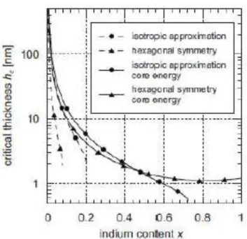
results poor performances in the InGaN solar cells [7], [8], [9]. Growing an InGaN layer (>100 nm) with high crystal quality remains a challenge (Figure 1.2-2) and
has severely limited the number of studies on p-GaN/i-InGaN/n-GaN heterojunction
8
Figure 1.2-2 The relationship between critical thickness and indium content ratio.
2. Lattice mismatch and defects : The III-nitride solar cells face important challenges
in lattice mismatch issue. The large difference in interatomic spacing between InN
and GaN results poor quality growth of InGaN, especially in the intermediate range
of In content . In general, a large lattice mismatch between InN and GaN and the
low temperature growth of InGaN detracts from the crystalline quality in epitaxial
layers and induces defects due to threading dislocation (TD), thereby generating
nonradiative recombination centers (NRCs) in the light absorbing layer.[14]
Furthermore, these defect centers trap and interact with photogenerated carriers,
thereby reducing the carrier lifetime and short-circuit current carrier of the solar
cells.[15]
3. Phase separation and In fluctuation and carrierdynamics : There are many
roadblocks to achieving efficient III-nitride PV devices. Foremost, growing high
quality InGaN layers with high indium compositions and the required thickness is
difficult, which is already discussed. Phase separation in InGaN layer is also among
9
formation of microscopic or macroscopic domains of variable constituent
composition in a material. Phase separation incorporates lower band gap domains
within the material that absorbs corresponding low energy light, its effect is
opposite to that of intermediate bands or quantum dots. As the size and distribution
of the lower bandgap phase-separated domains are not optimal, they act as
recombination centers decreasing the short circuit current of the solar cell. It is also
evident from the theory of quantum well solar cells [16] that the lower bandgap
material tends to dominate by pinning down the open circuit voltage of the device.
When the thickness and/or mole fraction of InxGa1−xN materials increase, In-rich
clusters in InGaN films easily induce phase separation. This leads to lower Voc
compared with theoretical values, low FFs, and large recombination rate by defect
states that degrade the Jsc of InGaN-based PV devices.
Although InGaN based solar cells offer tremendous potential for terrestrial as well as
space photovoltaic applications, there are only a few reports on InGaN based solar cells.
Furthermore, most reported InGaN solar cells have In contents lower than 15% and band gaps
near 3 eV, or larger, and therefore deliver diminishing quantum efficiency at wavelengths
longer than 420 nm.[17]-[21] An earlier theoretical material system to obtain solar cells
having a solar energy conversion efficiency greater than 50% can be fulfilled by InGaN alloys
with In content of about 40%.[22] Additionally, III-nitride multijunction solar cells with near
ideal band gaps for maximum solar energy conversion efficiency must incorporate InGaN
layers with higher In contents or lower energy band gaps. However, the realization of high
crystalline quality In- GaN films in the entire composition range is highly challenging. One of
the biggest problems is attributed to the large lattice mismatch between InN and GaN,
resulting in low solubility and phase separation.[23]-[24]
InGaN/GaN multiple quantum well solar cells is one way to improve lattice mismatch
10
order to enhance the absorption of the incident light.
1.3 Motivation
The high efficiency solar cells has become more and more important in the future.
Compared to Silicon-based solar cell, the GaN solar cell has higher efficiency and is
considered for future generation of photovoltaics applications. But due to the absorption range
of GaN/InGaN solar cells is short, otherwise the reflectance of GaN is over 20% without any
antireflection coating layer. So how to achieve the most use of the light will be an important
issue in GaN/InGaN solar cells.
So antireflection is a key technique for efficiently harvesting solar photon. Several
studies of nanostructure demonstrate it offer ultra-low reflectivity.
As mentioned before, the absorption range for GaN/InGaN solar cells is short. So how to
use the short wavelength region is an important thing to enhance the efficiency of InGaN/GaN
multiple quantum well solar cells. We observe the ITO will absorb the the light before 380nm.
That will cause a big loss.
In this study we will compare the flat InGaN/GaN multiple quantum well solar cells to
the nanostructured ones. We used textured PDMS film to reduce the reflectance without
making electricity property poor. We use a material called quantum dots (QDs) to solve the
problem of high absorption of front ITO layer. QDs will absorb the short wavelength light
11
Chaper 2. Basic Theories of Solar Cell
2.1 The fundamental structure of solar cell
A complete solar cell structure design was shown in Figure 2.1-1 [25]-[26], there is a
glass protective layer (cover glass) and a transparent adhesive layer outside, which play the
role of fixed and the protection of the internal components of solar cells are not damage by
the environment water vapor and other material. According to their function the internal
components of solar cell, they can be divided into three parts, the first one is the
anti-reflective layer (antireflection coating), which improve the light harvesting in solar cell
by the optical design further to reduce optical losses due to the reflection; The second one is
the semiconductor pn junction (active layer), the pn junction can absorb the light and
generate the electron-hole pair and then separate the electron and hole which diffuse to the
electric field the between the pn junction. The third one is electrode, which extract the carrier.
The front electrode which allows light to pass through so it will be designed into different
spacing and the rate of metal shielding finger patterns according to different cells, back
electrode which with the whole plane structure, and reflect the light which one is incomplete
absorbed at once optical path back to the active layer and increase the power conversion
efficiency. By using the load of outside circuit, the photocurrent can change into to an output
power. For enhancing the power efficiency of solar cell, there are three keys can be
improved.
(i) Enhancing the photon collection, the implementation is an anti-reflective layer, an
effective anti-reflective layer in solar cells which should have features of broadband
and omnidirectional anti-reflective characteristics, and increase the photo collection
per unit area of solar cells.
(ii) Enhancing the internal quantum efficiency (IQE), the implementation is
12
material defect at manufacturing process or reducing opportunity of the carrier
recombines by defect. Developing high-quality solar material or by epitaxial process
to create the most suitable structure for photovoltaic which improve the solar energy
conversion efficiency and has a broadband absorption spectrum.
(iii) Enhancing the electron extraction (Carrier collection), the implementation is to
develop a high-quality electrodes. The front electrode which allows light to pass
through, it will be designed into different spacing and the rate of metal shielding
finger patterns according to different cells further to enhance the electron extraction.
Another key point of electrode design is reducing the series resistance and forms an
ohmic contact to reduce the loss of carrier.
Figure 2.1-1 Illustrations of the fundamental structure of solar cell
2.2 The physics of solar cells
Typically, solar cell was formed as a diode, and there is a pn junction between the
n-type and p-type semiconductor, due to the different concentration of electron and hole,
carrier diffusion will occur and result in diffusion current. In the vicinity of the junction, the
electron concentration of n-type is higher than the electron concentration in p-type, so the
13
higher than the hole concentration in n-type, so the hole will diffuse form p-type to n-type, so
the neutral will be broken. The junction at the n-type side will exist the positive charges which
were caused by the donor, and the junction at the p-type side will exist the negative charges
which were caused by the acceptor. The region with n-type positive charges and p-type
negative charges which we called space charge region, and there is an electrical field in the
space charge region and the direction is from n-type side to p-type side.
When the light with the energy higher than the band gap of the semiconductor was
incident, the light will be absorbed then transfer the energy to electrons, and then the electron
are excited to a higher energy state which resulting in an electron - hole pairs. Due to the
built-in electrical fields the electrons will move to the n-type region and the holes will move
to the p-type region. The electron hole pairs move by the built-in electrical fields will result in
drift current.
The basic working principle of solar cells is separate the electron hole pairs by using the
built-in electrical field in the space charge region before they recombine. Figure2.2-1 shows
the diffusion mechanism and drift mechanism when the light incident into the solar cell, the
photocurrent is the sum of diffusion current and drift current [27]-[28]. If we make a contact
with two terminals in a diode, it is called short circuit and the current was called short circuit
current which equal to photocurrent. If there is no contact with two terminals in a diode, it is
called open circuit, when the light incident, the electron will accumulate at n-type side and the
hole will accumulate at p-type side which results in a photo-voltage or called open circuit
14
Figure 2.2-1 Illustrations of the carrier generation, carrier diffusion and carrier drift in solar cell
2.3 The parameter of solar cells
Figure 2.3-1 The diagram of solar cell equivalent circuit.
Figure 2.3-1 illustrates the equivalent circuit of solar cell. From this diagram, one could
find the photo-generated current (I) as follows[29]:
{ [
( )
] }
(2-1)
where Isc is the short-circuit current (also called light-generated current, IL), I0 is the reverse
15
degrees Kelvin, n is the ideality factor of diode (1<n<2, n=1 for the Shockley equation), Rs
is the equivalent series resistance and Rsh is the equivalent shunt resistance of the solar cell.
An idealized solar cell, the series resistance Rs is close to infinity and treats as open in the
equivalent circuit. Therefore, the Eq.(2-1) can simplified as:
[ (
) ]
(2-2)In Figure 2.3-1, when the intensity of solar radiation is weak, the current of diode is
approximately the leakage current (
), therefore, Rs can be ignore and Rsh effect is
important, then Eq. (2-1) can be rewritten as:
[ (
)]
(2-3)When the intensity of solar radiation is great, the light-generated current is great and
diode is on condition. Therefore, the current of diode is greater than the leakage current
(
), and the Rsh can be ignore and the Rs effect is important. Then the Eq. (2-1) can
be rewritten as:
[ (
) ]
(2-4)16
The I-V characteristics of solar cell in dark condition and under illumination were shown
in Figure 2.3-2 [30]. Four parameters are usually used to characterize the solar cell output
performances and shown in this figure. The parameters used to describe the solar cell
performances are indicated as follows [31]:
(1) Short-Circuit Current, Isc
Isc is a current when the solar cells were under illumination, and with a zero external load,
it means the solar cell circuit is short circuit. It is determined on the voltage (V) equal to zero
by Eq. (2-2). This is equal to the light-generated current IL ideally. As V=0, the Eq. (2-2) can
be written as:
(2-5)
(2) Open-Circuit Voltage, Voc
The open-circuit voltage is is a voltage when the solar cells were under illumination, and
with an infinite external load, it means the solar cell circuit is open circuit, at this time the
output current is zero. Voc can be solved in I=0 and V=Voc from Eq. (2-2), which is expressed
as:
(
)
(2-6)Voc is determined by the properties of the semiconductor by virtue of its dependence on
I0.
(3) Fill Factor, FF
Which is defined as the maximum ratio of the output power to the product on the
short-circuit current and open-circuit voltage, which can be expressed as:
(
)
(2-7)17
It is measure of how squareness the output characteristics are. For cell of reasonably efficiency, it has a value in the range 0.7 to 0.85.
(4) Conversion Efficiency, η
The conversion efficiency of solar cell is defined as the maximum ratio of the output
power to the input power, which can be expressed as
[ ( ) ] (2-8)
where Pin is the total power under the light incident to the cell.
The solar cell parameters such as open-circuit voltage Voc, short-circuit current Isc and
fill factor FF can provide the information about designing and improving the photodiode due
to their characteristics depended on the properties of the semiconductor materials and the
structure of device.
(5) Quantum Efficiency
Quantum efficiency (QE) is the ratio of the number of charge carriers collected by the
solar cell to the number of photons of a given energy shining on the solar cell. QE therefore
relates to the response of a solar cell to the various wavelengths in the spectrum of light
shining on the cell. The QE is given as a function of either wavelength or energy. If all the
photons of a certain wavelength are absorbed and we collect the resulting minority carriers
(for example, electrons in a p-type material), and then the QE at that particular wavelength
has a value of one. The QE for photons with energy below the band gap is zero.
The quantum efficiency ideally has a square shape, where the QE value is fairly constant
across the entire spectrum of wavelengths measured. However, the QE for most solar cells is
reduced because of the effects of recombination, where charge carriers are not able to move
18
the QE. For example, modifying the front surface can affect carriers generated near the
surface. And because high-energy (blue) light is absorbed very close to the surface,
considerable recombination at the front surface will affect the "blue" portion of the QE.
Similarly, lower energy (green) light is absorbed in the bulk of a solar cell, and a low
diffusion length will affect the collection probability from the solar cell bulk, reducing the QE
in the green portion of the spectrum. In somewhat technical terms, the quantum efficiency can
be viewed as the collection probability due to the generation profile of a single wavelength,
integrated over the device thickness and normalized to the number of incident photons.
"Quantum efficiency" is also sometimes called IPCE, which stands for
Incident-Photon-to-electron Conversion Efficiency.
Two types of quantum efficiency (QE) of a solar cell are often considered:
External Quantum Efficiency (EQE) is the ratio of the number of charge carriers collected by the solar cell to the number of photons of a given energy shining on the solar cell from
outside (incident photons).
Internal Quantum Efficiency (IQE) is the ratio of the number of charge carriers collected by the solar cell to the number of photons of a given energy that shine on the solar cell
from outside and are absorbed by the cell.
The IQE is always larger than the EQE. A low IQE indicates that the active layer of the
solar cell is unable to make good use of the photons. A low EQE can indicate that, but it can
also, instead, indicate that a lot of the light was reflected.
To measure the IQE, one first measures the EQE of the solar device, then measures its
transmission and reflection, and combines these data to infer the IQE.
19
In real cells power is dissipated through the resistance of the contacts and through
leakage currents around the sides of the device. These effects are equivalent electrically to
two parasitic resistances in series (Rs) and in parallel (Rsh) with the cell (Figure 2.3.3).
The series resistance arises from the resistance of the cell material to current flow,
particularly through the front surface to the contacts, and from resistive contacts. Series
resistance is a particular problem at high current densities, for instance under concentrated
light. The parallel or shunt resistance arise from leakage of current through the cell, around
the edges of the device and between contacts of different polarity. It is a problem in poorly
rectifying devices.
Series and parallel resistance reduce the fill factor as shown in Figure 2.3-3. For an
efficient cell we want Rs to be as small and Rsh to be as large as possible.
Figure 2.3-3 Effect of increasing series and reducing parallel resistances. In each
case the outer curve has Rs = 0 and Rsh = ∞. In each case the effect of the
resistances is to reduce the area of the maximum power rectangle compared to Jsc ×
20
Chaper 3.
Experimental Instruments and Measuring Instruments
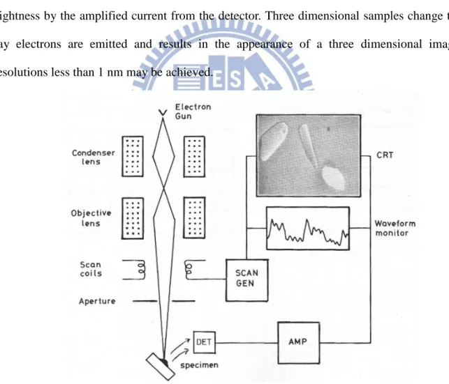
3.1 Scanning Electron Microsope (SEM)
A scanning electron microscope (SEM) is a type of electron microscope that images a
sample by scanning it with a high-energy beam of electrons in a raster scan pattern. The
electrons interact with the atoms that make up the sample producing signals that contain
information about the sample's surface topography, composition, and other properties such as
electrical conductivity.
The types of signals produced by an SEM include secondary electrons, back-scattered
electrons (BSE), characteristic X-rays, light (cathodoluminescence), specimen current and
transmitted electrons. Secondary electron detectors are common in all SEMs, but it is rare that
a single machine would have detectors for all possible signals. The signals result from
interactions of the electron beam with atoms at or near the surface of the sample. In the most
common or standard detection mode, secondary electron imaging or SEI, the SEM can
produce very high-resolution images of a sample surface, revealing details less than 1 nm in
size. Due to the very narrow electron beam, SEM micrographs have a large depth of field
yielding a characteristic three-dimensional appearance useful for understanding the surface
structure of a sample. This is exemplified by the micrograph of pollen shown to the right. A
wide range of magnifications is possible, from about 10 times (about equivalent to that of a
powerful hand-lens) to more than 500,000 times, about 250 times the magnification limit of
the best light microscopes. Back-scattered electrons (BSE) are beam electrons that are
reflected from the sample by elastic scattering. BSE are often used in analytical SEM along
with the spectra made from the characteristic X-rays. Because the intensity of the BSE signal
is strongly related to the atomic number (Z) of the specimen, BSE images can provide
information about the distribution of different elements in the sample. For the same reason,
21
otherwise be difficult or impossible to detect in secondary electron images in biological
specimens. Characteristic X-rays are emitted when the electron beam removes an inner shell
electron from the sample, causing a higher energy electron to fill the shell and release energy.
These characteristic X-rays are used to identify the composition and measure the abundance
of elements in the sample [32].
As the sample is scanned by the electron beam as shown in figure 3.1-1, it emits
electrons and electromagnetic radiation. A detector counts the low energy secondary electrons
(< 50 eV) or other radiation emitted. The image is produced by two dimensional intensity
distributions by scanning a cathode ray tube (CRT) spot onto a screen and modulating the
brightness by the amplified current from the detector. Three dimensional samples change the
way electrons are emitted and results in the appearance of a three dimensional image.
Resolutions less than 1 nm may be achieved.
22
3.2 Plasma-enhanced chemical vapor deposition (PECVD)
Plasma-enhanced chemical vapor deposition (PECVD) is a process used to deposit thin
films from a gas state (vapor) to a solid state on a substrate. Chemical reactions are involved
in the process, which occur after creation of a plasma of the reacting gases. The plasma is
generally created by RF (AC) frequency or DC discharge between two electrodes, the space
between which is filled with the reacting gases.
Plasma deposition is often used in semiconductor manufacturing to deposit films onto
wafers containing metal layers or other temperature-sensitive structures. Silicon dioxide can
be deposited from dichlorosilane or silane and oxygen, typically at pressures from a few
hundred millitorr to a few torr. Plasma-deposited silicon nitride, formed from silane and
ammonia or nitrogen, is also widely used, although it is important to note that it is not
possible to deposit a pure nitride in this fashion. Plasma nitrides always contain a large
amount of hydrogen, which can be bonded to silicon (Si-H) or nitrogen (Si-NH); this
hydrogen has an important influence on UV absorption, stability, mechanical stress, and
electrical conductivity.
Silicon Dioxide can also be deposited from tetraethoxysilane (TEOS) in an oxygen or
oxygen-argon plasma. These films can be contaminated with significant carbon and hydrogen
as silanol, and can be unstable in air. Pressures of a few torr and small electrode spacings,
and/or dual frequency deposition, are helpful to achieve high deposition rates with good film
stability.
High-density plasma deposition of silicon dioxide from silane and oxygen/argon has
been widely used to create a nearly hydrogen-free film with good conformality over complex
surfaces, the latter resulting from intense ion bombardment and consequent sputtering of the
23
3.3 Inductively-Coupled Plasma (ICP)
ICP etching system is dry etching system. The plasma region was crylindrical. This low
aspect ratio contributes to the high plasma production efficiency in that it reduced the ratio of
the plasma flux hitting the walls to the plasma flux hitting to the wafer. A circular array of
magnetic line cusps was used to aid in plasma confinement and improve uniformity. The
plasma was driven by a coil, separated from the plasma by a dielectric window.
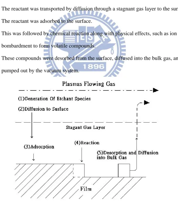
The plasma-assisted etching process proceeds in five steps as illustrated in Figure3.3-1.
1. The process began with the generation of the etchant species in the plasma.
2. The reactant was transported by diffusion through a stagnant gas layer to the surface.
3. The reactant was adsorbed to the surface.
4. This was followed by chemical reaction along with physical effects, such as ion
bombardment to form volatile compounds.
5. These compounds were desorbed from the surface, diffused into the bulk gas, and
pumped out by the vacuum system.
24
Here we use nanosphere spreaded on GaN to be mask etching by ICP-RIE to form some
nanostructure. We use Cl2/Ar to be the etching gas. By adding different ratio of the gas, we
can achieve different kinds of the nanoscale shape.
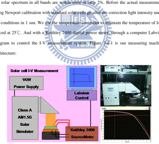
3.4 Current-voltage measurement (J-V curve)
Solar cell device characteristics measurement and analysis in the laboratory, set up by
self-complete measure machine architecture to achieve. We use the U.S. company
manufacturing Newport's AM1.5G 1000W Class A standard solar simulator, the United States
National Renewable Energy Laboratory (NREL) calibrated with international standards set by
the solar spectrum in all bands are within error of only 2%. Before the actual measurement,
using Newport calibration with standard solar cells go after the correction light intensity under
the conditions in 1 sun. We use the temperature controller to maintain the temperature of load
placed at 25℃. And with a Keithley 2400 digital power meter, through a computer Labview
program to control the I-V measurement system. Figure 3.4-1 is our measuring machine
architecture:
25
Energy conversion efficiency of solar cells is measured the I-V characteristics under
simulated sunlight illumination conditions (AM1.5G). We can learn about the important
parameters through the conversion efficiency of solar cells, including short-circuit current (Isc),
open-circuit voltage (Voc), fill factor (FF), power conversion efficiency (η), Maxima power
voltage (Vmax), Maxima power current (Imax), series resistance (Rs), and shunt resistance (Rsh).
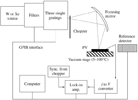
3.5 External quantum efficiency measurement (EQE)
Measuring the external quantum efficiency (QE (λ)), also known as spectral response (SR (λ)) is very important for understanding the carrier generation and the diffusion mechanism of photovoltaic device. The unit of spectral is the amperage of current generate
from per wattage of incident light (A / W). Formula 3-1 shows the mathematical formula of
external quantum efficiency, which indicate the probability of incident photon transform to
electron-hole pairs. hc qSR QE
) ( ) ( (3-1) We assume that the operating point of maximum power output and short-circuit arethe same, so usually the spectral response is the short circuit current. During solar cell
research there are several systems of external quantum efficiency measurement, such as
interference filter, grating spectrometer etc... For single-junction solar cells we use the
periodic single-frequency light to irradiate solar cell and measure the photocurrent then using
lock-in amplifier to transfer the signal into AC signal. In our experiment we use a grating
spectrometer system for broadband spectral measurements (400-3200 nm) and for high
spectral resolution, the setup is as figure 3.5-1[34]. Xenon lamp with wide spectrum when the
wide spectrum light pass through a grating it will become a single frequency light and then
focus on the solar cell. The aberration can be solved by using a spherical mirror or a parabolic
26
Figure 3.5-1 The schematic of grating quantum efficiency measurement system
3.6 Angle resolved Integrating sphere reflectance measurements
Figure 3.6-1(a) is a traditional reflectivity measurements diagram. When we want to
measure the reflectance of the smooth surface, the laser light is incident to the sample surface
by a specific angle. As the sample itself is a smooth surface, and the incident light is single
wavelength, we can obtain the reflected light at corresponding angle by the Snell’s law. At
this point we just put on a light detector on the path of the reflected light, and we can collect
the reflected light from the sample surface effectively. Thus it can measure the reflectance
27
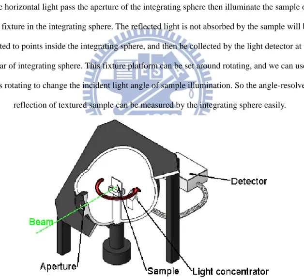
Figure 3.6-1 (a) Schematic diagram of conventional reflectivity measurements. (b) Schematic diagram of Integrating sphere reflectance measurements.
For the particles surface or rough samples, we also want to understand the different
wavelengths light reflectivity, so we change the incident light source to the Xe lamp light with
broadband spectrum. Figure 3.6-1(b) shows, when we made the surface of the textured
structure which the dimension size is closed to the wavelength of incident light, the different
wavelengths of light on the structure surface produce different levels of splitting, and at the
same time with a large number of light diffraction and scattering phenomenon, which will
make the direction of reflected light is no longer regularly, but from different angles toward
the divergent out. In such condition, if we still use previously measurement way which placed
a light detector in a particular direction, we will only receive a small portion of the reflected
light, so that out of the reflectance measurement is not an objective value. For rough surface
samples, in order to improve the problem of not only received light at a specific point, Fig.
3.6-1(b), our approach is coupled with an integrating sphere to collect the complete angle
28
sphere and were eventually collected by the light detector. And in order to analyze the
reflectivity of different wavelengths, we require a light detector which can detect wide
spectrum of light. By this way we obtained an objective of the reflectivity data, which
compared to the previous method of measuring reflectivity will be more realistic and accurate.
Figure 3.6-2 you can see the whole device roughly, we use Xe lamp as the light source to
simulate a wide spectrum of solar incident light, then light pass a convex lens by a guiding
fiber, this allows light to show about horizontal to pass the aperture of the integrating sphere.
The horizontal light pass the aperture of the integrating sphere then illuminate the sample on
the fixture in the integrating sphere. The reflected light is not absorbed by the sample will be
limited to points inside the integrating sphere, and then be collected by the light detector at the
rear of integrating sphere. This fixture platform can be set around rotating, and we can use
this rotating to change the incident light angle of sample illumination. So the angle-resolved
reflection of textured sample can be measured by the integrating sphere easily.
29
Chaper 4. Device fabrication and characteristics analysis
4.1 The fabrication of GaN/InGaN multiple quantum well solar cells
Figure 4.1-1 shows the fabrication flows of GaN/InGaN multiple quantum well solar
cells. As mentioned before, GaN/InGaN multiple quantum well solar cells is better than bulk
i-layer because we can grow higher content indium with thin thickness. So we decide to use
this type to grow our solar cell. The p-GaN 、 i-layer (GaN/InGaN multiple quantum well)、
n-GaN was deposited by Metal-organic Chemical Vapor Deposition (MOCVD) on sapphire
substrate. Then we use Plasma-enhanced chemical vapor deposition (PECVD) to grow
SiNx(Figure 4.1-1 (a)). After that, we use mask aligner and exposure system to define mesa
pattern and the Photo Resistor (PR) was used as mask immersed in Buffered Oxide Etch
(BOE) to remove some SiNx. Then we remove the rest PR by Acetone. The sample was
etching by Inductively-Coupled Plasma (ICP) with SiNx as mask. The p-n junction was
defined as figure 4.1-1(b). Then we use sputter to grow Indium tin oxide(ITO). After that, we
use mask aligner and exposure system to define ITO pattern and the PR was used as mask
immersed in aqua regia to remove some ITO(figure 4.1-1(c)). And the ITO on p-GaN was
used as Transparent conductive layer. Then we use mask aligner and exposure system to
define electrode pattern. We use E-gun to deposit our electrode. After that, we remove the PR
in acetone. Finally, the GaN/InGaN multiple quantum well solar cells is achieved. (figure
4.1-1(d)) The material and the thickness are in following tables.
Substrate p-type Active layer n-type Conducting
layer
electrode
sapphire p-GaN i-GaN/InGaN n-GaN ITO Cr
430um 200nm 112nm 1.5um 110nm 50nm
Table 4.1-1 The content and the thickness of our GaN/InGaN multiple quantum well solar cells
30
i-layer content thickness In (%)
Quantum well 14pair GaN/InGaN 5nm/3nm 16%
Table 4.1-2 The content and the thickness of i-layer.
Figure 4.1-1 The fabrication flows of GaN/InGaN multiple quantum well solar cells.
SiNx
p-GaN
i-layer
n-GaN
sapphire
ITO
electrode
31
4.2 Polydimethylsiloxane (PDMS)
Due to lots of defects caused by the dry etching process mentioned before, the electricity
properties must be poor. These defects will trap the electron-hole and decrease the efficiency.
So we found another material to reduce the Fresnel reflection which called
Polydimethylsiloxane (PDMS). The advantages of using PDMS film are the low-cost,
non-vacuum system and simple process (only spin coating and imprinting needed). Other than
ease of fabrication, PDMS film provides a refractive index gradient to serve as an
anti-reflection layer. Extra benefits of light trapping and scattering can be added when the film
is stamped with high texture pattern.
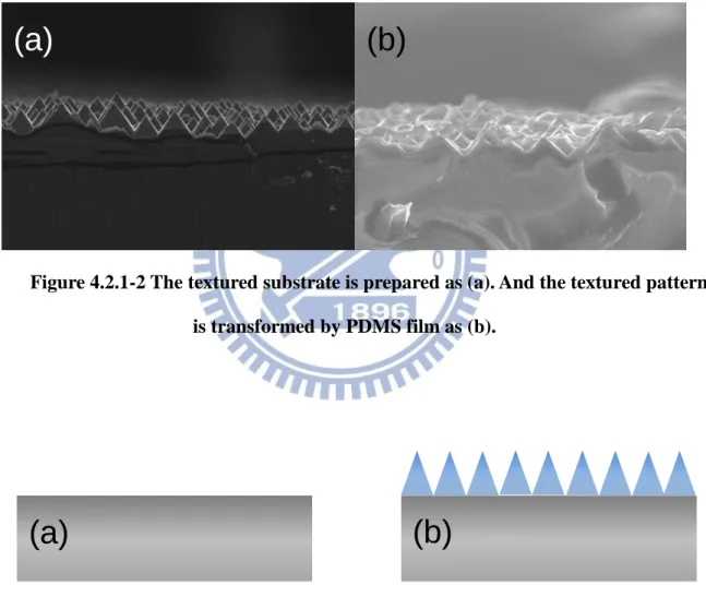
4.2.1 Fabrication process of textured PDMS film
To prepare a flexible textured PDMS film, a randomly textured crystalline silicon (c-Si)
mold-pattern was prepared by wet-etching with potassium hydroxide (KOH) [35]-[36], which
was used to imprint PDMS film(figure 4.2.1-1(a)), and the cross-sectional scanning electron
microscope (SEM) image of the randomly textured silicon substrate with a height of about 6
µm was shown Fig. 4.2.1-2(a). Second, the PDMS pre-polymer solution (in the form of a
viscous liquid) was dropped on randomly textured c-Si mold-pattern surface. Then, the spin
coating method was employed to form a uniformly PDMS polymer layer which can cover
over the c-Si mold-pattern(figure 4.2.1-1(b)), and then the substrate was baked at 70 ℃ for
half hour. After detaching from the c-Si mold, a flexible textured PDMS film was successfully
obtained(figure 4.2.1-1(c)) and the height of the textured structure was about 3 µm, as shown
32
(a) (b) (c)
Figure 4.2.1-1 The fabrication flows of rough PDMS film. Figure (a) is the textured substrate. Figure(b) is the PDMS spread on the substrate. Figure (c) is the rough PDMS
film.
Figure 4.2.1-2 The textured substrate is prepared as (a). And the textured pattern is transformed by PDMS film as (b).
Figure 4.2.1-3 The cell was shown in (a). And the textured PDMS film was put on cell as (b).
(a)
(b)
33
4.2.2 The optical properties analysis of PDMS film
We measure the optics properties of flat PDMS and textured PDMS. From the results,
the transmittance of both the flat and textured ones are very high(Figure 4.2.2-1). So it won’t
loss much energy. After that, we measure the Haze of both ones(Figure 4.2.2-2) , and the
definition formula is below(4-1). It means the ratio with transmittance of scattering light by
the total transmittance. From the figure, the haze of flat one is almost 0%, it means the light
go out from the flat PDMS in straight. Otherwise, the Haze of textured one is very high, it
means the light will scatter after go through the texture PDMS. And the optical path length is
getting longer, which is benefit for solar cell to absorb more light.
Figure 4.2.2-1 The transmittance of flat PDMS and rough PDMS.
300 400 500 600 700 800 900 1000 1100
0
20
40
60
80
100
Tr
a
nsistance
(%)
Wavelength (nm)
Flat PDMS
Rough PDMS
34
Figure 4.2.2-2 The haze of flat PDMS and rough PDMS.
(4-1)
In order to understand how the scattering light capability of the flexible textured and
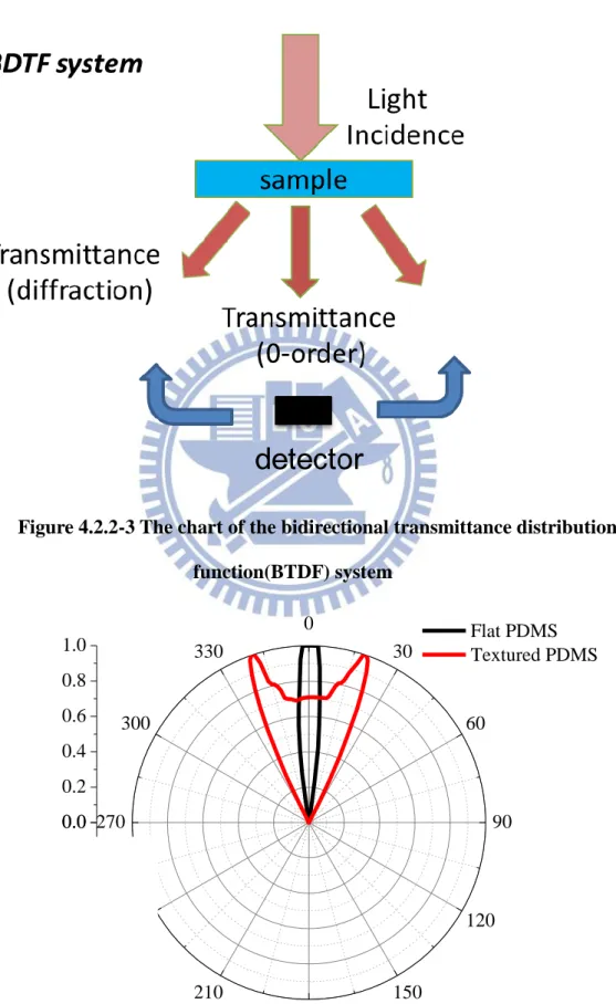
flat PDMS films, we first measured the angle-dependent intensity of transmittance by
bidirectional transmittance distribution function (BTDF) system with an incident light of 380
nm and ultraviolet-visible spectrophotometer. The system setup is shown in below(Figure
4.2.2-3). The light will go through the sample and scatter. And there is a detector moving as a
circle to receive the light. So we will know the intensity of the scattered light with the angle.
The results is shown in figure 4.2.2-4. The view angle of the flexible textured PDMS film at
the full-width at half-maximum was enlarged from 12° to 48° compared with the flat PDMS
film, which could be attributed to the increased light scattering by the textured structure as
shown in Fig. 4.2.2-4. As the results, the introduction of the flexible textured PDMS film can
𝐻𝑎𝑧𝑒(%)
𝑇
𝑑𝑖𝑓𝑓
𝑇
𝑡𝑜𝑡𝑎𝑙
500
1000
1500
2000
2500
0
20
40
60
80
100
Haz
e
(%)
Wavelength (nm)
Textured PDMS film
Flat PDMS film
35
deflect the photons in much wider angle and lengthen the traveling distance in the cell, which
implies higher possibility of getting absorbed.
Figure 4.2.2-3 The chart of the bidirectional transmittance distribution function(BTDF) system
Figure 4.2.2-4 The intensity and the corresponding angle of flat and rough PDMS.
0.0 0.2 0.4 0.6 0.8 1.0 0 30 60 90 120 150 180 210 240 270 300 330 0.0 0.2 0.4 0.6 0.8 1.0 Flat PDMS Textured PDMS