全電性自旋流量測的研究
96
0
0
全文
(2) 全電性自旋流量測. A STUDY ON AN ALL-ELECTRIC DETECTION OF SPIN CURRENT. 研 究 生:周昆宜. Student:Kun-Yi Chou. 指導教授:朱仲夏教授. Advisor:Prof. Chon Saar Chu. 國 立 交 通 大 學 電 子 物 理 研 究 所 碩 士 論 文 A Thesis Submitted to Department of Electrophysics College of Science National Chiao Tung University in Partial Fulfillment of the Requirements for the Degree of Master in Electrophysics. October 2009 Hsinchu, Taiwan, Republic of China. 中華民國九十八年十月.
(3) 全電性自旋流量測的研究 研究生:周昆宜. 指導教授:朱仲夏教授. 國立交通大學 電子物理研究所. 摘要. 我們提出了一種全電性量測交流自旋流(alternating spin current)的方法並且 理論計算出交流自旋流所產生的電信號。我們的系統主要利用半導體中的自旋軌 道交互作用,以平面二維電子氣(two-dimension electron gas)夾在兩個金屬閘極中 間作為測量裝置,在這樣結構中的電磁波為波導的模態。我們研究在自旋極化方 向與流動方向相互垂直並且躺在二維電子氣平面中的自旋流,這樣的交流自旋流 會激發出光子,只有對應於橫向磁場的波導模式(transverse magnetic modes)的光 子才被激發。光子在兩個閘極之間產生交替的電位差,而此電位差是可以用實驗 去量測的。. i.
(4) A STUDY ON AN ALL-ELECTRIC DETECTION OF SPIN CURRENT. Student: Kun-Yi Chou. Advisor:Prof. Chon Saar Chu. Department of Electrophysics National Chiao Tung University. Abstract We propose a pure electrical means of detecting an alternating (ac) spin current, and we perform theoretical calculations on the order of magnitude of the expected electrical signal. Our proposed scheme has employed the spin-orbit interaction in semiconductors. The proposed measurement device consists of a two-dimensional electron gas (2DEG) sandwiched between two metallic gates such that the electromagnetic waves in between the gates are waveguide modes. An ac in-plane spin current, with both spin and flow direction orthogonal to each other and in the plane of the 2DEG, passes through the structure is found to excite photons. Only photons corresponding to the transverse magnetic (TM) waveguide modes are excited. These excitations give rise to an ac electrical potential difference between the two metal gates. The potential difference is found to be measurable by present day experimental capability.. ii.
(5) 致謝 能夠完成碩士學位,我特別感謝朱老師兩年多來的諄諄教誨,不只是在知識上的 傳授,更重要的是處事的態度,以及學習的方法。也同樣感謝唐志雄學長、王律 堯學長、張榮興學長、江吉偉學長、邱志宣學長,幾位學長都曾多次幫我解答課 業與研究上的困難,還有謝謝小明和阿杜兩位同學,我們一起讀書相互勉勵。除 此之外更要謝謝爸爸、媽媽、哥哥和朋友的支持與鼓勵。. iii.
(6) Contents Abstract in Chinese. i. Abstract in English. ii. Acknowledgement. iii. 1 Introduction. 1. 1.1. Introductory touring to this thesis . . . . . . . . . . . . . . . . . . . . . . .. 1. 1.2. Background and Review . . . . . . . . . . . . . . . . . . . . . . . . . . . .. 2. 1.3. Motivation . . . . . . . . . . . . . . . . . . . . . . . . . . . . . . . . . . . .. 6. 1.4. Introduction to calculation method . . . . . . . . . . . . . . . . . . . . . .. 7. 2 Geometric structure of the system we consider. 10. 2.1. Structure of our system . . . . . . . . . . . . . . . . . . . . . . . . . . . . . 10. 2.2. Quantization of electromagnetic wave in waveguide . . . . . . . . . . . . . 12. 2.3. Brief summary . . . . . . . . . . . . . . . . . . . . . . . . . . . . . . . . . 20. 3 Examination of the calculation method we consider. 21. 3.1. Charge oscillation in free space . . . . . . . . . . . . . . . . . . . . . . . . 21. 3.2. EM wave generated by oscillating line charge current in waveguide . . . . . 27. 3.3. Brief summary . . . . . . . . . . . . . . . . . . . . . . . . . . . . . . . . . 37. 4 The electric field induced by ac spin current 4.1. 38. Effective Hamiltonian for photon . . . . . . . . . . . . . . . . . . . . . . . 38 iv.
(7) CONTENTS 4.2. The new photon state in the waveguide . . . . . . . . . . . . . . . . . . . . 43. 4.3. The expectation value of the vector potential in our system . . . . . . . . . 44. 4.4. Brief summary . . . . . . . . . . . . . . . . . . . . . . . . . . . . . . . . . 49. 5 Result and discussion. 50. 5.1. Discussion . . . . . . . . . . . . . . . . . . . . . . . . . . . . . . . . . . . . 50. 5.2. Injection of in-plane AC spin current . . . . . . . . . . . . . . . . . . . . . 53. 5.3. Conclusion . . . . . . . . . . . . . . . . . . . . . . . . . . . . . . . . . . . . 57. A Average over direction. 58. B The complex integral I. 62. C Approximation between wave function of current and vector potential 65 D The complex integral II. 68. E The derivation of electric field induced by ac line current in classical calculation. 74. F The complex integral III. 77. v.
(8) List of Figures 2.1. An illustration of the geometry of the two parallel-planes waveguide. The 2DEG which is formed at the intersection of two kind of semiconductor with different band gap energies is at the middle of the waveguide. . . . . . 11. 2.2. If the ac in-plane spin current oscillates toward x-direction on 2DEG and the spin polarized direction toward negative y-direction, it will generate ac electrical potential difference between the two metal gates. . . . . . . . . . 11. 2.3. The two parallel-planes waveguide consists of a dielectric material with permeability µ and primitivity ε sandwiched by two parallel metal gates with conductivity σ (σ → ∞). . . . . . . . . . . . . . . . . . . . . . . . . . 14. 2.4. ˆ The picture shows the relation between zˆ, xˆ0 , yˆ0 , and k.(We set a reference coordinate, xˆ0 -ˆ y 0 coordinate, which is in the x-y plane.) . . . . . . . . . . . 14. 3.1. The particle carrying electric charge q with is deposited at the origin, and it acts as simple harmonic oscillation with frequancy Ω and amplitude a. . 22. 3.2. An infinite long wire is located at the middle of the waveguide and towards the x-direction. . . . . . . . . . . . . . . . . . . . . . . . . . . . . . . . . . 28. 3.3. The side view of the waveguide structure and the wire. The waveguide is the same as one we discussed in 2.2 which has permeability µ and primitivity ε. The up and down electrode slabs are made of perfect conductor. . . . . 28. 3.4. ˆ and zˆ × k. ˆ . . . . . . . 31 The illustration shows the relation between φk , k,. 4.1. The figure shows the relationship between φk , k, and xˆ. . . . . . . . . . . . 40 vi.
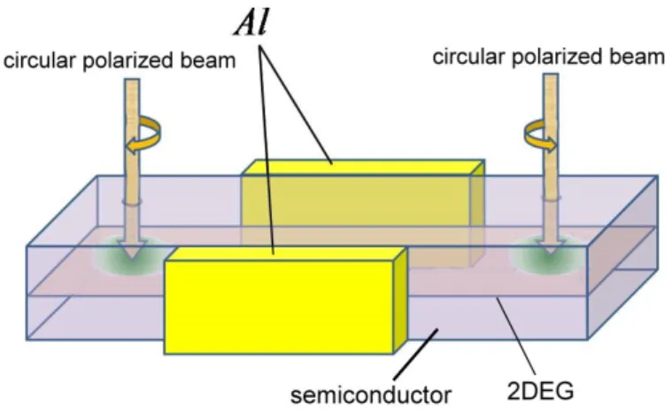
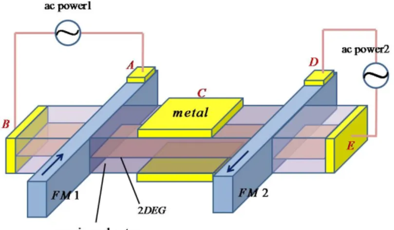
(9) LIST OF FIGURES 5.1. The spin current is injected from the both sides of the waveguide. We apply an external electronic filter with high quality vector Q to increase the output signal by several order.. 5.2. . . . . . . . . . . . . . . . . . . . . . . 53. The illustration of the optical spin injection for our system. Right- or left-hand circular polarized electromagnetic wave to illuminate the 2DEG normally and then generate spin accumulation.Spins will diffuse away due to concentration imbalance and cause spin current. Right- and left-hand alternating circular can drive ac spin current diffusing away. The metal gates of waveguide are deposited at both side of the device and detect the electrical potential difference. The two beams with opponent right- and left-hand alternating circular polarization on the left and right side of the system can enhance the spin current. . . . . . . . . . . . . . . . . . . . . . 54. 5.3. The ac charge current is injected from the both terminals, and the charge current with spin-polarization flows through the waveguide. These spinpolarized electrons originate from the ferromagnetic probes.. 5.4. . . . . . . . . 55. When we drive charge current between A,B and D,E, it will resulting in nonequilibrium spin accumulation in the ferromagnets that diffused away from the injection point. If we drive ac charge current, it will drive ac spin current into the waveguide structure. . . . . . . . . . . . . . . . . . . . . . 56. ˆ zˆ00 , xˆ00 , yˆ00 , zˆ. kˆ = zˆ00 , and the λ is A.1 The figure shows the relationship of k, in the xˆ00 -ˆ y 00 plane. yˆ00 is normal to the xˆ00 -ˆ z 00 plane. . . . . . . . . . . . . . 59 A.2 The figure shown the relation of yˆ0 , xˆ0 , zˆ0 , and rˆ. The zˆ direction is in the yˆ0 -ˆ z 0 plane and θ is the angle between rˆ and zˆ.. . . . . . . . . . . . . . . . 60. B.1 The counter-clockwise contour we choose closes the upper half plane and has one pole at (−Ω, iη) in it. . . . . . . . . . . . . . . . . . . . . . . . . . 64 D.1 The contour we separate into five section closes the upper-half plane except the branch point at z 0 = ikz and the branch cut (red arrow). . . . . . . . . 69 vii.
(10) LIST OF FIGURES F.1 The illustration shows the contour we choose in Eq. (F.1) on the complex plane of z 0 . The contour can be separated with five sections, Γ1 , Γ2 , Γ3 , Cr , CR . z0 q z 0 2 +kz 2. exp[iΩt]. has two branch points located at z 0 = ikz and )−iη+Ω ( z 0 = −ikz respectively on the complex plane. The red allows are the branch 1 µε. z 0 2 +kz 2. cuts we choose. . . . . . . . . . . . . . . . . . . . . . . . . . . . . . . . . . 78 q F.2 There are still two poles at ± µε (Ω2 + i2ηΩ) − kz 2 which we do not show here. The section of integral Γ1 is the integral from negative infinity to infinity x. The two red arrows are the cut lines which are from the points ikz and − ikz respectively to infinity and negative infinity. . . . . . . . . . 81. viii.
(11) Chapter 1 Introduction To start this first chapter of this thesis, we provide in Sec. 1-1, a general guide to the structure of the thesis. The next two sections of this introductory chapter cover the background and motivation of this thesis. The last section describes our calculation method in this thesis.. 1.1. Introductory touring to this thesis. In the first chapter, we introduce the background of spintronics as well as spin-orbit interaction, and we propose the motivation of this issue and the calculation method in this thesis. Chapter 2 describes the geometric structure of our system and the quantization of electromagnetic wave confined by the waveguide. In Chapter 3, we solve two traditional electrodynamics problems with our calculation method, for checking if our method is practical. In Chapter 4, we solve the electric field induced by ac in-plane polarized spin current. Chapter 5 reports that the signal generated by ac in-plane polarized spin current is measurable. Finally, we discuss and take conclusions in this thesis.. 1.
(12) CHAPTER 1. INTRODUCTION. 1.2. Background and Review. In this review section, we present a brief background on spintronics, on spin current, on spin-orbit interaction, and on the progress in the research on the measurement of spin current. Spintronics Spintronics is an area of intense current scientific interests[1]. It is important for information storage and quantum computing. Fundamental studies of spintronics include investigations of spin transport in materials, as well as measurement of spin accumulation, spin relaxation, and spin current. Especially, spin current plays an important role in an spintronic devices. Our work in this thesis focus on measurenent of spin current. We must understand the definition of spin current before our work. Spin current In this paragraph, we explain the definition of spin current. An electron carries both charge and spin which may have two components: up and down. In the semi-classical picture, spin can be described by a unit vector. Traditional charge current is a flow of electron which is the sum of flows of up- and down-spin electrons. The spin information may be neglected in charge current. A spin current differs from a charge current. For a simple description, spin current can be recognized as the difference between the flows of up and down spin electrons. A pure spin current means that equivalent up and down spin flows in the opposite direction. There is no net particle transfer across any cross section of the channel. Measuring spin current in solid state systems provides a new tool to investigate the mesoscopic system, and it also give us hopes that it could be applied in spintronics and quantum information processing in the future. We can say that measurement of spin current is an indispensable part in field of spintronics. It has been found that spin-orbit interaction can be a nice tool to measure spin current all. 2.
(13) CHAPTER 1. INTRODUCTION electrically. In the following two subsections we will introduce spin-orbit interaction in an atom and in semiconductor respectively. Spin-orbit interaction in an atom Spin-orbit interaction is a well-known phenomenon which is caused from the interaction of a particle’s spin with its own motion. A particle in an electric field experiences an effective magnetic field in its co-moving frame. For electrons, it brings about lifting of the degeneracy of energy levels of electrons according to their spin states. In atomic physics, this interaction comes from the electron spin magnetic moment interacting with the magnetic moment due to the orbit motion of the electron. In nonrelativistic approximation to Dirac equation, the form of the spin-orbit interaction term in an atom is given by:. HSO,vac = −. e~ σ · (p × E) , 4m0 2 c2. (1.1). where e is the magnitude of electron charge(e > 0), ~ is the Plank’s constant, m0 is the mass of a free electron, c is the light speed in vacuum, σ = (σx , σy , σz ) are the Pauli matrices , p is the momentum of the spin, and E is the electric field that the electron travels through in the atom[2]. When the electron velocity is far less than the speed of light and a small electric field is quite small, the Dirac gap 2m0 c2 ≈ 1M eV in the denominator of Eq. (1.1) is too large that the spin-orbit interaction in a single atom is quite week. We may rewrite equation Eq. (1.1) as HSO,vac = −e Λvac σ·(p × E) , where Λvac = ~. ~2 4m0 2 c2. is the spin-orbit coupling constant in vacuum. Actually, spin-orbit interaction in vacuum or in a single atom has the same coupling constant, but the electric field comes from different sources. In a atom, electric field comes from the atomic nucleus. In vacuum, the electric field comes from the divergence of the potential in space. Even though the spin-orbit coupling in a single atom or in vacuum is very week, it will be magnified in. 3.
(14) CHAPTER 1. INTRODUCTION semiconductor. Spin-orbit interaction in semiconductor Spin-orbit interaction in solid state physics have the same form as Eq. (1.1) but difference in the spin-orbit coupling due to the energy gap difference. In semiconductor, spin-orbit coupling may be enhanced with several orders. The coupling strength is mostly derived from the electrons with high velocity under the strong electric field near the core of the atoms, rather than the weak velocity movement. Due to the periodicity of crystal, the electron energy spectrum form energy band structure in the reciprocal vector space. If the crystal system does not have the space inversion symmetry, the band gap will be narrower which result in stronger spin orbit coupling. In GaAs, the spin-orbit coupling constant 2 Λ is about 82.5 ˚ A which is seven order magnitude greater than Λvac . The perturbing. spin-orbit coupling Hamiltonian in GaAs may be written as: Λ HSO,sc = e σ · (p × E) , ~. (1.2). where Λ is the spin-orbit coupling constant in GaAs. The strength of spin-orbit interaction un semiconductor is manifestly seven order higher in magnitude than that in vacuum such that it becomes a nice tool to detect spin current electrically. Next, we will introduce kinds of principle means of detection of spin current. Review of measurement of spin current Generally, there are three kinds of principle means of detection of spin current. Here, we review some of them. The first method is mechanical measurement[3, 4]. In 2007, E. B. Sonin demonstrates that an equilibrium spin current in two-dimension electron gas (2DEG) with Rashba interaction which is one kind of spin-orbit interaction will lead to a mechanical torque on a substrate near an edge of the Rashba medium[4]. If the substrate is flexible enough. 4.
(15) CHAPTER 1. INTRODUCTION that the torques would distort it, it is a method to detect equilibrium spin currents experimentally that he measure the degree of contortion. Optical detection is also a general way to measure spin current[5–7]. In 2008, J. Wang, B. F. Zhu, and R. B. Liu described the first non-invasive method of measure pure spin current directly by a polarized light beam [7]. The polarized light beam which act as a ’photon spin current’ will interact with spin current due to the spin-orbit coupling without the Rashba or the Dresselhaus effect. The interaction result in linear and circular optical birefringence. They utilized the birefringence effects to measure to pure spin currents. The third one is electrical detection[8–12]. In 1985, Mark Johnson and R. H. Silsbee performed the experiment in non-magnetic aluminum strip contacted to two ferromagnetic electrodes[11]. They reported that injecting charge current from one of ferromagnetic electrodes into aluminum strip results in non-equilibrium spin accumulation at the interface of aluminum strip and the source ferromagnetic electrode. The spin accumulation defuses away from the interface and forms spin current. If there is a non-equilibrium spin accumulation in the vicinity of the detector, an open-circuit voltage will be developed across the interface. In 2006, S. O. Valenzuela and M. Tinkham demonstrate electrical detection of spin currents in metallic nanostructures. They apply reciprocal spin Hall effect in a diffusive metallic conductor and obtain its spin Hall conductivity. Finally they measure the laterally induced voltage which results from the conversion of the injected spin current into charge imbalance owing to the spin-orbit coupling. There are still Some other means of electrical detection of spin current proposed in resent years including theoretical and experimental proposition. It is worth to mention that in 2004, Qing-feng Sun et al. propose a journal named ”spin-current induced electric field” [12]. In that article, the authors investigate properties of the induced electric field of a steady-state spin-current without charge current. They regard one electron spin as a magnetic dipole. Such magnetic dipole current will generate electric field in space. They claim that a spin current with drift velocity 10−2 m/s flowing in an infinitely long wire with cross section area of 2 mm × 2 mm and the magnetic moment is perpendicular to the current direction. 5.
(16) CHAPTER 1. INTRODUCTION The spin current causes the potential difference∼ 12 µV at distance -1.1 mm and 1.1 mm on either side of the wire. It is a novel method to measure spin current by measuring the voltage directly induced by spin current. Even though the potential difference their report is measurable, the spin current is up to 640.82 Ampere. That is very giant magnitude of spin current. It is extremely difficult to generate such strong current in the thin wire.. 1.3. Motivation. In Sec. 1-2, we mentioned the paper which is proposed by Sun et al.[12] and based on the calculation of electrodynamics and relativity. They utilized the potential difference induced by magnetic dipole current to detect spin current. The spin-orbit interaction strength can be enhanced up to six orders of magnitude in semiconductor rather than in vacuum. We think that if spin current flows in semiconductor, we may think that it could induce more strongly electric field than in vacuum. It may be a power tool to measure spin current by detecting the potential difference induced by spin current. But it is very hard both to take the advantages of spin-orbit interaction in semiconductor and to use the calculation method of electrodynamics simultaneous. We can not find any equation corresponding to the enhanced strength of spin-orbit interaction in electrodynamics. However from the hamiltonian Eq. (1.2), we may take the advantages of spin-orbit interaction in semiconductor and calculate the potential difference induced by ac spin current in semiconductor from the viewpoint of photons. In addition, from equation Eq. (1.2), we support that the spin polarized direction, the direction of spin flow, and electric field induced by ac spin-polarized current are perpendicular to each other. Therefore, we want to design a device which can detect the ac electrical potential difference generate by ac spin polarized current, and two parallelplanes waveguide is the best choose. The two parallel-planes waveguide is not only easyfabricated but also measures the electrical potential difference easily. If the spin polarized direction and the ac in-plane spin flow is parallel to the metal gates of waveguide and they. 6.
(17) CHAPTER 1. INTRODUCTION are perpendicular to each other, it will generate electric field which is perpendicular to the metal gates of the waveguide. In this thesis, we propose that the ac spin current which flowing in 2DEG which is at the middle of the two metal gates of a two parallel-planes waveguide can induced electrical signal. This signal is measurable if we add appropriate external circuit.. 1.4. Introduction to calculation method. Our calculation is based on non-degenerate perturbation theorem. The calculation starts from the perturbing spin-orbit interaction term of the Hamiltonian. Λ H 0 = e σ · (p × E) , ~. (1.3). where e is the magnitude of electron charge (e > 0), Λ is the spin-orbit interaction constant in semiconductor, ~ is the Plank constant, σ = (σx , σy , σz ) are the Pauli matrices , and E is the electric field in the waveguide. While we consider that the second quantization procedure is applied to quantum field theory, the classical field variables become quantum operators [13]. In classical mechanics, the coordinates and momenta of a classical system can specify its state. In ordinary quantum mechanics, the position and the momentum of a single particle promoted to operators because the observables of position and the momentum can be quantized. The ordinary quantum mechanics can only deal with the number of conserved particle systems. However, in relativistic quantum mechanics, particles can be generated and annihilated. The mathematical formulations of ordinary quantum mechanics no longer apply. We must dealing with the creation and annihilation of particles with second quantization which is the establishment of relativistic quantum mechanics and quantum field theory. Second quantization method can deal with natural and simple symmetry of identical particles and anti-symmetry. Essentially, if we can stand in the viewpoint of electron to solve the problem with electromagnetic methods, but it is difficult to calculate. That is why we 7.
(18) CHAPTER 1. INTRODUCTION solve the problem with second quantization method. When we sandwich the perturbing Hamiltonian H 0 with the states of the oscillating spin polarized electron state |ψi, we can obtain the equivalent perturbing Hamiltonian H 0 ef f for the photons which emitted by the oscillating spin current between the parallel slabs. The effective Hamiltonian is given by: Λ H 0 ef f = hψ| e σ · (p × E) |ψi . ~. (1.4). Because the momentum p is an operator for electron, it act on the photon state. And the ”E” in Eq. (1.4) is the operator for photons and it does not act on the electron state. Applying time-dependent perturbation theory, we will obtain the first order perturbation coefficient. That is (1) fnkλ. −i = ~. Z. t. h{0, 0, ..., 0, 1nkλ , 0, ..., 0}| H 0 ef f |{0}idt0 ,. (1.5). −∞. where the subscript nkλ indicate the mode number. And we get the eigenstate state of first order approximation of the photons. It is given by:. |Ψi = |Ψ0 i +. X. (1). fnkλ |{0, 0, ..., 0, 1nkλ , 0, ..., 0}i ,. (1.6). nkλ. where |Ψ0 i is the initial photon state which is one of the eigenststes of unperturbed Hamiltonian. |Ψi is the new state after the H 0 is added to our system. It means that the photon state changes from |Ψ0 i to |Ψi when the ac spin current is applied. The photon eigetstate tells us all information of the photons of our system which we want to know. Then we sandwich the vector potential in the parallel plate capacitor with the the photon state |Ψi. A (r, t) = hΨ| A(op) |Ψi. (1.7). 8.
(19) CHAPTER 1. INTRODUCTION The result A (r, t) is the expectation value of vector potential in the parallel-plates waveguide in the photon state |Ψi. If we choose the transverse gauge, by taking A (r, t) partial derivative with respect to t, the electric field between the two parallel slabs could be obtained easily. By integrating the electric field, what we obtain is the ac electrical potential difference between the two metal gates. The potential difference is induced by ac spin current and is also what we want to know.. 9.
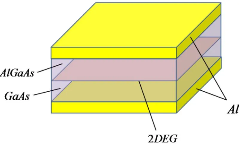
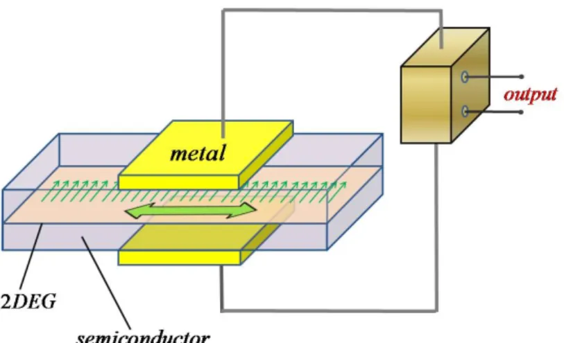
(20) Chapter 2 Geometric structure of the system we consider In this chapter, we will introduce the geometric structure of our system and derive the quantized electromagnetic wave in waveguide.. 2.1. Structure of our system. In this section, we show the geometric structure of our system. The model of our system is shown as Fig. 2.1. In chapter 5, we will demonstrate that this device can detect electric potential difference induced by ac in-plane polarized spin current by adding appropriate external electric circuit. At the middle of the device there is an extremely thin layer of 2DEG which is formed at the intersection of two kind of semiconductor with different band gap energies. Two pieces of metal gates sandwich the semiconductor structure and are parallel to the 2DEG. These two metal gates are used to detect the electrical potential difference and they construct a two-parallel-planes waveguide. We can apply two layers with two different ratios of Al to Ga of aluminum gallium arsenide (AlGaAs) as dielectric material between the two metal slabs to form 2DEG, and use aluminum slabs as gate to detect the electrical potential. 10.
(21) CHAPTER 2. GEOMETRIC STRUCTURE OF THE SYSTEM WE CONSIDER. Figure 2.1: An illustration of the geometry of the two parallel-planes waveguide. The 2DEG which is formed at the intersection of two kind of semiconductor with different band gap energies is at the middle of the waveguide.. Figure 2.2: If the ac in-plane spin current oscillates toward x-direction on 2DEG and the spin polarized direction toward negative y-direction, it will generate ac electrical potential difference between the two metal gates.. difference. We had discussed that electric field induced by ac spin-polarized current is perpendicular to the spin polarized direction and the oscillation direction of ac spin current. If we can generate pure ac in-plane polarized spin current on the 2DEG, which the spin 11.
(22) CHAPTER 2. GEOMETRIC STRUCTURE OF THE SYSTEM WE CONSIDER polarized direction is towards the negative y-direction, oscillating in x-direction shown as Fig. 2.2, we may measure the ac electrical potential difference between two metallic slabs. The waveguide structure can lead the far field to near field if the thickness of waveguide is comparable with the wave length of field. In our problem here, the propagating direction of the field radiated by ac spin current happens to be parallel to the field direction, because the electric field, spin polarized direction and current direction are perpendicular to each other. Thus we need to use a description different from that for the oscillating electric dipole because near field near field behavior is important. The waveguide modes provide us a naturel and appropriate scheme to describe the near field, which is very important for our case. Furthermore its upper and lower metal gates can also be electrodes to measure the ac electrical potential difference induced by the ac spin current. If we can figure out the correlation between the electrical potential difference and the magnitude of spin current, we may declare that we can detect ac in-plane polarized spin current by electric means.. 2.2. Quantization of electromagnetic wave in waveguide. Electromagnetic wave confined by a waveguide is different from that in vacuum. In this section we will deduce the quantization of electromagnetic wave in the waveguide. Quantization of electromagnetic wave in free space In chapter1, we discussed why we utilize the second quantization manner to deal with the field induced by ac spin current. The quantization of radiation field in free space is described in many textbooks [14]. The free radiation field is the quantized electromagnetic field inside an optical cavity with dimension L (L → ∞). If we want obtain the mathematics form of vector potential, in an intuitive picture, we can start from Maxwell’s equations in the absence of currents and charges. Then we can 12.
(23) CHAPTER 2. GEOMETRIC STRUCTURE OF THE SYSTEM WE CONSIDER obtain the vector potential in free space in transverse gauge in which the electric scalar potential is equal to zero and the vector potential A (r, t) is divergence-free. One way to obtain the quantized radiation field in free space is to identify the amplitudes of the vector potential A (r, t) with the annihilation or creation operators of harmonic oscillators. In interaction representation A(op) (r, t) develops in time by: A(op) (r, t) =. X kλ. (op). Akλ λ. exp (−ik · r + iωkλ t) exp (ik · r − iωkλ t) (op) + √ √ + Akλ λ∗ , V V. (2.1). where V = L3 is the free space volume and the vector λ is the polarization of the plane (op). (op) +. wave. k is the wave vector of the radiation field. Akλ and Akλ. are corresponding. to creation and annihilation (raising and lowering) operators respectively. The subscript (op). λ (λ = 1 or 2) of Akλ denotes two orthogonal polarization. When they act on eigenstate of photon, we can write down the relations: r (op) Akλ. |Nk1 λ1 , Nk2 λ2 , ...., Nkλ , ...i =. ~ p Nkλ |Nk1 λ1 , Nk2 λ2 , ...., Nkλ − 1, ...i , (2.2) 2ε0 ωkλ. r (op) + Akλ. |Nk1 λ1 , Nk2 λ2 , ...., Nkλ , ...i =. ~ p Nkλ + 1 |Nk1 λ1 , Nk2 λ2 , ...., Nkλ + 1, ...i , 2ε0 ωkλ (2.3). where Nkλ is the number of photons in the mode k, λ and ε0 is the permittivity in vacuum. (op). When Akλ applies on photon state , it reduces the number of photons in the mode kλ (op) +. by one. Akλ. applies on photon state , it increase the number of photons in the mode. kλ by one. Quantization of electromagnetic wave in waveguide Now we will derive the electromagnetic wave in the waveguide which is constructed with two metal plates , and a thick dielectric slab with thickness d and its dielectric constant. 13.
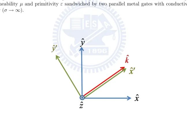
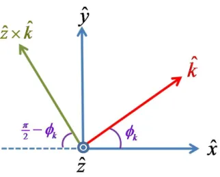
(24) CHAPTER 2. GEOMETRIC STRUCTURE OF THE SYSTEM WE CONSIDER. Figure 2.3: The two parallel-planes waveguide consists of a dielectric material with permeability µ and primitivity ε sandwiched by two parallel metal gates with conductivity σ (σ → ∞).. ˆ Figure 2.4: The picture shows the relation between zˆ, xˆ0 , yˆ0 , and k.(We set a reference 0 0 coordinate, xˆ -ˆ y coordinate, which is in the x-y plane.). and magnetic permeability are ε and µ respectively. The dielectric slab is sandwiched by the two plates. We assume the metal slabs are perfect conductor. The structure of the waveguide is shown as Fig. 2.3. We assume that the total electromagnetic wave propagate along the k-direction (note. 14.
(25) CHAPTER 2. GEOMETRIC STRUCTURE OF THE SYSTEM WE CONSIDER that kˆ = xˆ0 ) in dielectric layer, and the two metal plates are put z = 0 and z = d. And we assume zˆ × xˆ0 = yˆ0 . The relation between zˆ, xˆ0 , yˆ0 , and kˆ is shown in Fig. 2.4. We just consider about the plane waves, and it means B ∝ e−iωt and E ∝ e−iωt where is the angular frequency of incident wave and. ∂ ∂y 0. → 0. From Faraday’s law, we can get. ∂ B = iωB. We may write down the three components of Faraday’s law as ∇ × E = − ∂t. the following. −. ∂ Ey0 = iωBx0 , ∂z. (2.4). ∂ ∂ Ex0 − 0 Ez = iωBy0 , ∂z ∂x. (2.5). ∂ Ey0 = iωBz , ∂x0. (2.6). ∂ Considering Ampere’s law, we obtain ∇ × B = µε ∂t E = −iωµεE. Then we obtain the. following three differential equations.. −. ∂ By0 = −iωµεEx0 , ∂z. (2.7). ∂ ∂ Bx0 − 0 Bz = −iωµεEy0 , ∂z ∂x. (2.8). ∂ By0 = −iωµεEz . ∂x0. (2.9). Considering Maxwell equations, for two pieces of slab of waveguide which are made of perfect conductor, we have two boundary condition derived by Faraday’s law and divergence free of magnetic field. They are Bz = 0 at z = 0 and z = d Ex0 , Ey0 = 0 at z = 0 and z = d. The Eq. (2.4), Eq. (2.6), Eq. (2.8) only have variables Ey0 , Bx0 , and Bz . They can construct a wave equation called TE wave equation. The name ”TE” means transverse. 15.
(26) CHAPTER 2. GEOMETRIC STRUCTURE OF THE SYSTEM WE CONSIDER electric field. The wave equation is given by: µ. ¶ ∂2 ∂2 2 + + ω µε Ey0 = 0. ∂x0 2 ∂z 2. (2.10). Solving Eq. (2.10) by separation of variables, finally, we have: 0. Ey0 = E0 sin (kz z) eikx0 x , where E0 is the amplitude of the electric field, kx0 is the x0 -component wave number, and kz =. mπ , d. m = 0, 1, 2, 3, .... Magnetic field is transverse or perpendicular to the propagation direction. The fields are calculated to be. −. kz ∂ 0 Ey0 = iωBx0 → Bx0 = i E0 sin (kz z) eikx0 x , ∂z ω. k x0 ∂ 0 Ey0 = iωBz → Bz = E0 sin (kz z) eikx0 x . 0 ∂x ω m is the mode number which starts from one . kz and kx0 are satisfied with the dispersion relation kz 2 + kx0 2 = ω 2 µε. The Eq. (2.5), Eq. (2.7), Eq. (2.9) contain variables Ex0 , Ez , and By0 . The three differential equations can construct a wave equation called TM wave equation (Magnetic field is transverse or perpendicular to the propagation direction.). The wave equation is: µ. ¶ ∂2 ∂2 2 + + ω µε By0 = 0. ∂x0 2 ∂z 2. (2.11). Solving Eq. (2.11), we obtain 0. By0 = B0 cos (kz z) eikx0 x ,. where kz =. nπ , d. n=0,1,2,3, ..., kx0 is the x0 -component wave vector, and B0 is the amplitude. 16.
(27) CHAPTER 2. GEOMETRIC STRUCTURE OF THE SYSTEM WE CONSIDER of the magnetic field. Magnetic field is perpendicular to the electric field, and the fields are calculated to be. −. ∂ kz 0 By0 = −iωµεEx0 → Ex0 = i B0 sin (kz z) eikx0 x , ∂z ωµε. ∂ k x0 0 0 = −iωµεEz → Ez = − B0 cos (kz z) eikx0 x , B y 0 ∂x ωµε and we get the dispersion relationkz 2 + kx0 2 = ω 2 µε. Actually, kz is the transverse wave vector and k is the effectively longitudinal component of the wave vector. We already derived electromagnetic wave modes in parallel-plates waveguide. For real physical quantity, we may add its complex conjugate to the fields. Furthermore, we know that the wave in an arbitrary parallel-plate waveguide is not a plane wave, because a plane wave cannot satisfy the appropriate boundary conditions at the waveguide walls. But the modes can be expressed as a sum of plane waves. In general, we decompose the total electric field in the waveguide for different modes and different k as infinite (Fourier) superposition of all modes as given by For TE modes:. E=−. X m,k. sin. ³ mπ ´ © ´ ª³ z bmk ei(k·ρ−ωmk2 t) + bmk ∗ e−i(k·ρ−ωmk2 t) zˆ × kˆ d. (2.12). ³ mπ ´ ¡ X · 1 ³ mπ ´ ¢ cos z −ibmk ei(k·ρ−ωmk2 t) + ibmk ∗ e−i(k·ρ−ωmk2 t) kˆ B= ωmk2 d d m,k (2.13) ¸ ³ mπ ´ ¡ ¢ k sin z bmk ei(k·ρ−ωmk2 t) + bmk ∗ e−i(k·ρ−ωmk2 t) zˆ − ωmk2 d For TM modes, we have B = By0 yˆ0 = −. X n,k. cos. ³ nπ ´ © ´ ª³ z cnk ei(k·ρ−ωnk1 t) + cnk ∗ e−i(k·ρ−ωnk1 t) zˆ × kˆ , (2.14) d. 17.
(28) CHAPTER 2. GEOMETRIC STRUCTURE OF THE SYSTEM WE CONSIDER ³ nπ ´ ¡ X · 1 1 ³ nπ ´ ¢ sin z −icnk ei(k·ρ−ωnk1 t) + icnk ∗ e−i(k·ρ−ωnk1 t) kˆ E= µε ωnk1 d d n,k . (2.15) ¸ ³ nπ ´ ¡ ¢ 1 k i(k·ρ−ωnk1 t) ∗ −i(k·ρ−ωnk1 t) + zˆ cos z cnk e + cnk e µε ωnk1 d The dispersion relation is kz 2 + k 2 = ω 2 µε. bm (cn ) denotes the amplitude of the electric field for the m-th (n-th) mode. The time-dependence is given by putting in the whole plane wave: eik·ρ → ei(k·ρ−ωt) . The summation k contains all direction as well as all magnitude. ˆ We also change the notation ω into ωmk2 (ωnk1 ), because the frequency depends on kcomponent (kˆ = xˆ0 ) of wave number and mode number m(n). The other subscript of ωmk2 (ωnk1 ), 1 or 2, indicates TM or TE modes respectively. The electric field and vector potential respect to the relationship E = −∇φ −. ∂A ∂t. It’s. easy to derive the vector potential, if we choose the transverse gauge. For TE modes, the vector potential is given by:. A=−. X m,k. 1 iωmk2. ³ mπ ´ © ´ ª³ ∗ −i(k·ρ−ωmk2 t) i(k·ρ−ωmk2 t) ˆ sin z bmk e − bmk e zˆ × k . (2.16) d. For TM modes, we have: ³ nπ ´ ¡ X · 1 1 ³ nπ ´ ¢ i(k·ρ−ωnk1 t) ∗ −i(k·ρ−ωnk1 t) ˆ sin z c e + c e k A= − nk nk 2 µε ω d d nk1 n,k (2.17) ¸ ³ nπ ´ ¡ ¢ 1 k cos z −icnk ei(k·ρ−ωnk1 t) + icnk ∗ e−i(k·ρ−ωnk1 t) zˆ . + µε ωnk1 2 d Canonical quantization (also called second quantization) asks that the classical field variable becomes a quantum operator. The amplitude of vector potential cnk (bmk ) or cnk ∗ (bmk ∗ ) is corresponded to annihilation or creation operator respectively. Because cnk ∗ (bmk ∗ ) becomes operator, it may be wrote as cnk + (bmk + ). When cnk (bmk ) acts on the photon state, it will removes one photon with the mode nk (mk). cnk + (bmk + ) acts on an energy eigenstate, it will increase one photon with the mode nk (mk) ( Here ”n” or ”m” indicates the n-th mode in TM wave or the m-th mode in TE waves respectively.). Using cnk (bmk ) or cnk ∗ (bmk ∗ ) to describe the classical electromagnetic energy in a 18.
(29) CHAPTER 2. GEOMETRIC STRUCTURE OF THE SYSTEM WE CONSIDER volume V , we find the energy for TE modes inside the volume V is given by: Z Eenergy =. ¸ X 1 2 1 2 |bmk |2 V. dr εE + B =ε 2 2µ m=1,2,3,... ·. (2.18). By the same way, for TM modes we have. Eenergy =. 1 X |cnk |2 V. µ n=0,1,2,3,.... (2.19). Actually, in quantum theory the radiation energy is given by:. Eenergy = N ~ω,. (2.20). where N is the number of photons in the volume V, and is the angular frequency of these photons. Combining Eq. (2.18), Eq. (2.19), and Eq. (2.20), we have the dimension of the four coefficients. When they act on the eigenstate of electromagnetic field, we have: r bmk |Nm1 k1 2 , Nm2 k2 2 , ..., Nmk2 , ...i =. ~ωmk2 p Nmk2 |Nm1 k1 2 , Nm2 k2 2 , ..., Nmk2 − 1, ...i , εV (2.21). r bmk + |Nm1 k1 2 , Nm2 k2 2 , ..., Nmk2 , ...i =. ~ωmk2 p Nmk2 + 1 |Nm1 k1 2 , Nm2 k2 2 , ..., Nmk2 + 1, ...i , εV (2.22). r cnk |Nn1 k1 1 , Nn2 k2 1 , ..., Nnk1 , ...i =. µ. ~ωnk1 p Nnk1 |Nn1 k1 1 , Nn2 k2 1 , ..., Nnk1 − 1, ...i , V (2.23). r cnk + |Nn1 k1 1 , Nn2 k2 1 , ..., Nnk1 , ...i =. µ. ~ωnk1 p Nnk1 + 1 |Nn1 k1 1 , Nn2 k2 1 , ..., Nnk1 + 1, ...i , V 19.
(30) CHAPTER 2. GEOMETRIC STRUCTURE OF THE SYSTEM WE CONSIDER (2.24). where Nnκ1 (Nmk2 ) is the number of photons in the TM (TE) mode n (m) , k. We have found out the quantized radiation field in the waveguide. With the result, we can correctly calculate the radiation field generate by spin current or else radiation problem in the waveguide.. 2.3. Brief summary. Our system essentially comprises 2DEG which is formed at the AlGaAs/GaAs heterointerface and sandwiched by two piece of Al electrodes outermost. When ac in-plane spin current flows on the 2DEG, we utilize waveguide structure to detect the potential difference induced by the spin current. The quantized field in two-parallel-planes waveguide can be divided into two kinds of modes , TM modes and TE modes. Electric field in TE modes is perpendicular to the propagation direction of the beam and there is no electric field in the direction of propagation. Electric field in TM modes is perpendicular to the propagation direction.. 20.
(31) Chapter 3 Examination of the calculation method we consider In this chapter, we want to check if our calculation method is practical. We propose two problem of electrodynamics to compare the result which is solved by method of classical electrodynamics and the result solved by our method. The first problem is electromagnetic (EM) wave generated by single charge oscillation in free space. The second one is EM wave induced by oscillating charge current carried by an infinite long wire in waveguide.. 3.1. Charge oscillation in free space. In electrodynamics, the charge oscillation will generate electromagnetic wave in space. Using the method we proposed in Chapter 1, we calculate electric field generated by the charge oscillation in free space. We can also obtain the EM wave with Jefimenko’s equations which describe the behavior of the electric and magnetic fields in terms of the charge and current density at retarded times. Then we compare the result by this method with the result by the method of electrodynamics. If both the results are identical with each other, we confirm that our method is practical. We start from a charge oscillating along the z direction with the frequency Ω and the amplitude ”a” in the Cylindrical. 21.
(32) CHAPTER 3. EXAMINATION OF THE CALCULATION METHOD WE CONSIDER. Figure 3.1: The particle carrying electric charge q with is deposited at the origin, and it acts as simple harmonic oscillation with frequancy Ω and amplitude a.. coordinate. The equilibrium point of the charge is deposited at the origin shown as Fig. 3.1. We can write down the time-dependent position of the charge as the following: rp = a cos (Ωt) zˆ Effective Hamiltonian of photons The perturbation operator of charge-photon interaction is given by H 0 = −qE · r where E is the electric field[14]. If we just consider about the transverse field, the field induced by charge oscillation is the same as dipole oscillation with identical frequency and amplitude. In quantum mechanics, even though we cannot describe both position and momentum of an electron, we still recognize the oscillating charge as a classical particle. If the amplitude ”a” is much smaller than the wavelength of the light, the field can be recognize as far field. For relativity far field, because the oscillator is placed at origin, we can replace E (r, t) by E (0, t) because the charge oscillating at origin. H 0 ef f = −qE (0, t) · rp. (3.1). ∂A (0, t) · rp , =q ∂t 22.
(33) CHAPTER 3. EXAMINATION OF THE CALCULATION METHOD WE CONSIDER where c is the light speed in vacuum , q is the electric charge of the particle, A is the vector potential in transverses gauge . Incorporating Eq. (2.2) into Eq. (3.1) , and then the perturbing Hamiltonian becomes. H. 0. ef f. ¾ X½ exp (+ickkλ t) exp (−ickkλ t) (op) + (op) ∗ √ √ + ckkλ Akλ (λ · rp ) , = iq −ckkλ Akλ (λ · rp ) V V kλ (3.2). where V is the free space volume and λ is the polarization of the plane wave. k is the (op) +. (op). wave vector of the radiation field. Akλ and Akλ. are corresponding to creation and (op). annihilation operators respectively. The subscript λ (λ = 1 or 2) of Akλ denotes two orthogonal polarization. The photon eigenstate For spontaneous emission, the oscillator emits only one photon. The initial state must be |Ψ0 i = |{0k1 λ1 , 0k2 λ2 , ..., 0kλ , .., }i (or we can write as|{0}i) and the final state is |{0, 0, ..., 0, 1kλ , 0, ..., 0}i. The initial state is also one of the unperturbed eigenstates. H 0 ef f is identified as time dependant perturbing Hamiltonian. Applying first-order perturbation theory, the first order perturbation coefficient is given by (1) fkλ. −i = ~. Z. t. h{0, ..., 0, 1kλ , 0, ...}| H 0 ef f |{0}idt,. −∞. where ~ is the Plank constant. Essentially, the strength of perturbing Hamiltonian H 0 is weak enough, so we can apply perturbation theorem. Assuming the limit of a very slow switch on, H 0 ef f eηt with η which is far smaller than 1, so H 0 ef f switched on very gradually in the past. We can then take the initial time to be −∞, and the first order perturbation coefficient becomes: (1) fkλ. −i = ~. Z. t. h{0, ..., 0, 1kλ , 0, ...}| H 0 ef f eηt |{0}idt. −∞. 23. (3.3).
(34) CHAPTER 3. EXAMINATION OF THE CALCULATION METHOD WE CONSIDER We consider one photon emittion. It means the photon state from |{0}i to |{0, ..., 0, 1kλ , 0, ...}i. Substituting equation Eq. (3.2) into Eq. (3.3), we obtain:. (1) fkλ. q = ~. Z. X½. t. h{0, ..., 0, 1kλ , 0, ...}| −∞. (op) + ckk0 λ0 Ak0 λ0. ¡. k0 λ0. ¾ ¢ exp (+ickk0 λ0 t) ηt √ λ · rp e |{0, ..., 0}idt0 . V 0∗. (3.4) (op). Here we used the character of annihilation operator Ak0 λ0 |{0, 0, ..., 0}i = 0. Solving Eq. (3.4), we can rewrite the first order perturbation coefficient is (1) fkλ. q = ~. r. ~ωkλ 1 1 √ a (λ∗ · zˆ) {(η + ickkλ ) cos (Ωt) + Ω sin (Ωt)} 2ε0 V (η + ickkλ )2 + Ω2 (3.5). × exp [(η + ickkλ ) t] The eigenstate of the photon is changed to |Ψi after we consider about the perturbation of the system H 0 ef f . |Ψi is given by:. |Ψi = |{0, 0, ..., 0, ..., 0}i +. X. (1). fkλ |{0, 0, ..., 0, 1kλ , 0, ..., 0}i. (3.6). kλ. The expectation value of vector potential The photon state describes all information about photons in the waveguide including the vector potential in space. The expectation value of the magnetic vector potential in the state |Ψi is given by: A (r, t) = hΨ| A(op) |Ψi ( =. h{0, 0, ..., 0, ..., 0}| +. X k00 λ00. +. X. ) (1). +. f k00 λ00 h{0, 0, ..., 0, 1k00 λ00 , 0, ..., 0}| A(op) {|{0, 0, ..., 0, ..., 0}i ). (1). fk0 λ0 |{0, 0, ..., 0, 1k0 λ0 , 0, ..., 0}i. k0 λ0. (3.7). 24.
(35) CHAPTER 3. EXAMINATION OF THE CALCULATION METHOD WE CONSIDER (op) +. Akλ. is an operator that increases the number of photons in the mode kλ by one. When (op) +. (op). the operators Akλ and Akλ. are applied to the photon state, they obey the Eq. (2.2) and. Eq. (2.3), respectively. And the expectation value of the vector potential of the system becomes. A (r, t) =. X. r. kλ. ¾ ½ + (1) exp (ik · r − iωkλ t) ∗ (1) exp (−ik · r + iωkλ t) √ √ + λ f kλ . (3.8) λfkλ 2ωkλ ε0 V V ~. Putting Eq. (3.5) into Eq. (3.8), the vector potential leads to ¾ exp (iΩt) exp (−iΩt) + exp [ik · r] λz λ A (r, t) = 4V ε0 Ω + ck − iη ck − Ω − iη kλ ½ ¾ X qa (i) exp (−iΩt) exp (+iΩt) ∗ + exp [−ik · r] λz λ + . 4V ε0 Ω + ck + iη ck − Ω + iη kλ X qa (−i). ½. ∗. (3.9). We notice that the second term in above equation is complex conjugate of the first term. Now we take average over polarization. By taking linear polarization, we have λ∗ = λ. Then, we have ¾ n ³ ´ o ½ exp (iΩt) exp (−iΩt) ˆ ˆ A (r, t) = + exp [ik · r] zˆ − k · zˆ k 4V ε Ω + ck − iη ck − Ω − iη 0 k ½ ¾ (3.10) ´ o exp (−iΩt) n ³ X qa (i) exp (+iΩt) ˆ ˆ + exp [−ik · r] zˆ − k · zˆ k + . 4V ε Ω + ck + iη ck − Ω + iη 0 k X qa (−i). The summation over k means summing over arbitrary direction and magnitude of wave number k. k must be continuous, so we may change the representation of the summation to representation of integration. It means X. →. X ∆kx ∆ky ∆kz. ∆kx ∆ky ∆kz Z Z Z 1 1 V 2 → dkx dky dkz = ³ ´ ³ ´ ³ ´ k dkdΩk = k 2 dkdΩk , 3 2π 2π 2π (∆kx ) (∆ky ) (∆kz ) (2π) k. k. Lx. Ly. 25. Lz.
(36) CHAPTER 3. EXAMINATION OF THE CALCULATION METHOD WE CONSIDER where Li (i=x,y,z) is length which an quantum state occupies, and Ωkˆ is the solid angle. Z h ³ ´ i V qa (−i) 2 ˆ exp (ik · r) z ˆ − k · z ˆ kˆ A (r, t) = k dkdΩ k 3 4V ε (2π) 0 ½ ¾ Z exp (iΩt) exp (−iΩt) V qa (i) × + + k 2 dkdΩk 3 Ω + ck − iη ck − Ω − iη 4V ε0 (2π) ¾ h ³ ´ i ½ exp (−iΩt) exp (+iΩt) ˆ ˆ × exp (−ik · r) zˆ − k · zˆ k + . Ω + ck + iη ck − Ω + iη We deal with the angular integral. 1 4π. R. (3.11). dΩk first. The detail of calculation is complex, and. it will save for Appendix A. After average over direction, the vector potential becomes: ´ V qa ³ ˆ θ sin θ A (r, t) = 2π 8V ε ½Z ∞ 0 µ ¶· ¸ − exp [ikr] + exp [−ikr] exp (iΩt) exp (−iΩt) 2 k dk × + (3.12) kr Ω + ck − iη ck − Ω − iη k=0 µ ¶ · ¸¾ Z ∞ exp [ikr] − exp [−ikr] exp (−iΩt) exp (+iΩt) + k 2 dk + . kr Ω + ck + iη ck − Ω + iη k=0 Using the relationship. Ra 0. f (x)dx =. R0 −a. f (−x)dx, and making the change of variables,. u0 = ck we can obtain : " £ ¤ £ 0r¤ ´Z ∞ − exp iu0 rc cqa ³ ˆ exp (iΩt) 0 2 − exp iu c A (r, t) = θ sin θ u + 16π 2 ε0 c4 u0 rc u0 + (Ω − iη) u0 rc u0 =−∞ £ ¤ exp −iu0 rc exp (iΩt) exp (−iΩt) × 0 + r 0 0 u − (Ω + iη) uc u + (Ω − iη) # £ ¤ exp −iu0 rc exp (−iΩt) du0 + r 0 0 uc u − (Ω + iη) (3.13). Using residue integral method , the vector potential can be derived as :. A (r, t) = −. ´ ³ qa Ω ³ ˆ r´ θ sin θ sin Ωt − Ω 4πc2 ε0 r c. (3.14). The detailed complex integral of equation is preserved in Appendix B. It’s easy to obtain the electric field after we get the result of the complex calculation. Because we choose 26.
(37) CHAPTER 3. EXAMINATION OF THE CALCULATION METHOD WE CONSIDER the transverse gauge, the electric scalar potential is equal to zero. ∂ A ∂t ³ qa Ω2 r´ ˆ = (sin θ) cos Ωt − Ω θ 4πc2 ε0 r c. E (r, t) = −∇V −. (3.15). Here, we only consider about the transverse field and neglect Coulomb field. The field is identical with the far electric field induced by dipole antenna. From above equation, we can realize that the frequency of the field is Ω which is the same as the frequency of the oscillating electron. If the charge wiggles back and forth, the higher the frequency, the shorter the waves, because it have less time to get out of the way before the charge changes its direction. This result which we use semi-classical calculation method is the same as the result which we use calculation method of classical electrodynamics. The two results obtained by different calculation methods are the same. It implies our assumption that our oscillating charge radiates light with one photon can match the oscillating charge problem. Also, our method is practical to be use for calculating spin current problem.. 3.2. EM wave generated by oscillating line charge current in waveguide. In the same way, we solve the electric field induced by ac line charge current in waveguide with the method we consider, for checking if our calculation method is practical, again. The calculation also gives us a simpler exercise for solving electric field induced by ac in-plane polarized spin current. When the wave length becomes comparable with the thickness of the waveguide, we should consider the near-field light instead of far-field light. The waveguide structure confines the field and leads far-field into near-field wave. The near-field wave is more complicated than far-field wave. Fortunately, plane wave expansion method is useful method for us to deal with our problem. Therefore, the quantization field in two-parallel-. 27.
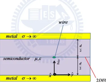
(38) CHAPTER 3. EXAMINATION OF THE CALCULATION METHOD WE CONSIDER. Figure 3.2: An infinite long wire is located at the middle of the waveguide and towards the x-direction.. Figure 3.3: The side view of the waveguide structure and the wire. The waveguide is the same as one we discussed in 2.2 which has permeability µ and primitivity ε. The up and down electrode slabs are made of perfect conductor.. planes waveguide we derived in Chapter 2 can be a complete set. The structure of the waveguide we consider about is the same as we discussed in Chapter 2. An infinite long wire parallel with x-axis is located in the middle of two parallel metal gates as shown the following picture.. 28.
(39) CHAPTER 3. EXAMINATION OF THE CALCULATION METHOD WE CONSIDER Assume that the semiconductor between two metal gates has the permittivity ε and permeability µrespectively. The wire is very thin, comparing with the distance d, and e xˆ where λe is the particle density per this wire carries flow of electron charge I = eλe ~k me. unit length, me is the mass of a free electron, and ke is the electron wave number, where ~ is the Plank constant. The wave function of the electrons is. Ψ (r) = hr|ψi =. p λe exp [ike x] ϕ (y, z) .. (3.16). At the beginning, we do not consider about ac current. We will add the oscillating information in the effective Hamiltonian later. The perturbation operator of oscillating line current in the waveguide is given by: H0 =. e e e (p · A + A · p) = p·A= A · p, 2me me me. (3.17). where e > 0. For the transverse gauge p · A − A · p = −i~∇ · A = 0. We care about only the transverse field without the longitudinal field. It means that we consider about the field induced by ac charge current without the Coulomb field. Therefore, the perturbing Hamiltonian does not include the Coulomb potential. Effective Hamiltonian We sandwich Eq. (3.17) with electron state to get the effective Hamiltonian of the photons in the waveguide which is given by the following: e H 0 ef f = hψ| H 0 |ψi = hψ| A · p |ψi me ½Z Z Z Z Z Z e e = ke ~λe dx dy dzϕ (y, z) Ax ϕ (y, z) − i~λ dx dy dzϕ (y, z) me me ¾ Z Z Z ∂ ∂ × Ay ϕ (y, z) + dx dy dzϕ (y, z) Az ϕ (y, z) , ∂y ∂z (3.18). 29.
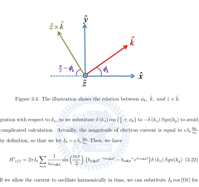
(40) CHAPTER 3. EXAMINATION OF THE CALCULATION METHOD WE CONSIDER where Ax , Ay , Az is the x, y, z-component of vector potential respectively. Vector potential ¢ ¡ near the position x, y = 0, z = d2 changes violently, but the wave function of the electron ϕ (y, z) changes smoothly, so we may take some approximation. Then we have:. H. 0. ef f. e = ~λe me. ¾ ½ Z Z ¢ 1 ¢ ¡ ¡ ∂ d d ke dxAx x, 0, 2 − i dx Ax x, 0, 2 . 2 ∂x. (3.19). The detailed derivation from Eq. (3.18) to Eq. (3.19) is left in the Appendix C. Putting Eq. (2.16) and Eq. (2.17) into Eq. (3.19), we obtain: (. H. 0. ef f. ". Z ³ mπ ´ X½ 1 e 1 −iωmk2 t = ~λe · ke − bmk sin e bmk + dxeikx x − me iωmk2 2 iωmk2 m,k Z ³ ´ ³ nπ ´ ³ mπ ´ 1 1 ³ ³ nπ ´ eiωmk2 t dxe−ikx x } zˆ × kˆ · xˆ − c sin × sin nk 2 µε ωnk1 2 d 2 ¶ ¸ Z Z ³ nπ ´ ³ nπ ´ 1 × e−iωnk2 t dxeikx x +cnk + sin eiωnk2 t dxe−ikx x kx − i [ d 2 2 Z ³ mπ ´ ³ X ½ ikx ikx mπ ´ − bmk sin e−iωmk2 t dxeikx x + bmk + sin iωmk2 2 iωmk2 2 m,k ¾ Z ³ nπ ´ ³ nπ ´ ³ ´ 1 1 ³ iωmk2 t −ikx x ˆ ×e dxe ikx cnk sin e−iωnk2 t zˆ × k · xˆ − 2 µε ωnk1 d 2 ¶ ¸¾ Z Z ³ nπ ´ ³ nπ ´ sin eiωnk2 t dxe−ikx x kx . × dxeikx x −ikx cnk + d 2 (3.20). According to Fourier analyze,. R∞ −∞. eikx x dx = 2πδ (kx ). The terms with kz δ (kz ) in the. equation above will be vanished after integration overkx . We can drop it. Then we have H. 0. ef f. · ³ mπ ´ 1 ~ke X 2π bmk sin e−iωmk2 t δ (kx ) = −eλe me iω 2 mk2 m,k ¸ ³ mπ ´ ³π ´ 1 + iωmk2 t − bmk sin e δ (kx ) cos + φk , iωmk2 2 2. (3.21). where φk is the angle between the k and xˆ. The relationship between φk , k, and xˆ is shown in Fig. 3.4 ¢ ¡ ”δ (kx ) cos π2 + φk ” in equation above will lead to the form ”−Sgn(ky )” after inte-. 30.
(41) CHAPTER 3. EXAMINATION OF THE CALCULATION METHOD WE CONSIDER. ˆ and zˆ × k. ˆ Figure 3.4: The illustration shows the relation between φk , k,. gration with respect to kx , so we substitute δ (kx ) cos. ¡π 2. ¢ + φk to −δ (kx ) Sgn(ky ) to avoid. e complicated calculation. Actually, the magnitude of electron current is equal to eλe ~k me e by definition, so that we let I0 = eλe ~k .Then, we have me. H. 0. ef f. = 2πI0. X. 1. m,κ. iωmk2. sin. ³ mπ ´ © 2. ª bmk2 e−iωmk2 t − bmk2 + eiωmk2 t δ (kx ) Sgn(ky ) (3.22). If we allow the current to oscillate harmonically in time, we can substitute I0 cos (Ωt) for I0 where Ω is the oscillation angular frequency. The perturbation operator becomes: H 0 ef f = 2πI0 cos (Ωt). X. 1. m,κ. iωmk2. sin. ³ mπ ´ © 2. bmk2 e−iωmk2 t − bmk2 + eiωmk2 t. ª (3.23). × δ (kx ) Sgn(ky ) The first order perturbation coefficient Again, we apply time-dependent perturbation theory to solve the new eigenstate of photon, and the first order perturbation coefficient in H 0 ef f is given by: (1) fkλ. −i = ~. Z. t. h{0, 0, ..., 0, 1kλ , 0, ..., 0}| H 0 ef f |{0}idt.. −∞. 31. (3.24).
(42) CHAPTER 3. EXAMINATION OF THE CALCULATION METHOD WE CONSIDER We impose the mechanism of adiabatic turn-on to simulate the more realistic system and simplify calculation. Therefore, we put the term eηt in the integration form. We consider about one photon emission. It means the photon state from |{0}i to |{0, 0, ..., 0, 1kλ , 0, ..., 0}i We add a factor of to describe adiabatic turned on . η is a constant smaller than 1 far, switched on very gradually in the past, and we are looking at times much smaller than η1 . We can then take the initial time to be −∞. For TE modes We have the first order perturbation coefficient by: (1) fm0 κ0 2. Z e −i t h{0, 0, ..., 0, 1mk2 , 0, ..., 0}| A · peηt |{0}idt = ~ −∞ m Z t i = eηt h{0, 0, ..., 0, 1mk2 , 0, ..., 0}| I0 cos (Ωt) 2πi (3.25) ~ −∞ ³ mπ ´ © X 1 ª sin bmk e−iωmk2 t − bmk + eiωmk2 t δ (kx ) Sgn(ky ) |{0}i dt × ωmk2 2 m,k. bmk and bmk2 + in Eq. (3.25) is corresponded to the annihilation operator and the creation operator respectively. We use Eq. (2.21) as well as Eq. (2.22) and Simplify Eq. (3.25), so we have: (1) fmk2. r ³ mπ ´ 1 I0 ~ωmk2 sin = 2π ~ ωmk2 εV 2 (3.26) ½ ¾ 1 exp [i (ωmk2 − iη + Ω) t] exp [i (ωmk2 − iη − Ω) t] × + δ (kx ) Sgn(ky ) 2i ωmk2 − iη + Ω ωmk2 − iη − Ω. For TM modes (1) fn0 k0 1. −i = ~. Z. t. h{0, 0, ..., 0, 1n0 k0 1 , 0, ..., 0}| H 0 ef f |{0}idt = 0.. −∞. The expectation value of vector potential We are interesting the expectation value of vector potential, because the electric field can be obtained easily after knowing it. The time-dependent expectation value of vector. 32.
(43) CHAPTER 3. EXAMINATION OF THE CALCULATION METHOD WE CONSIDER potential in the photon state |Ψi is given by: A (r, t) = hΨ| A(op) |Ψi = {h{0, 0, ..., 0, ...}| + +. X. X. (1) ∗. f mk2 h{0, ..., 0, 1mk2 , 0, ...}|}A(op) {|{0, 0, ..., 0, ...}i. mk (1). fmk2 |{0, ..., 0, 1mk2 , 0, ...}i}.. mk. (3.27) (1). (1). Let’s remember that fnk1 is equal to zero, and we already derived fmk2 in Eq. (3.26). We combine Eq. (2.16), Eq. (3.26) and Eq. (3.27), and we get: A (r, t) ³ mπ ´ ³ mπ ´ ½ X I0 1 ~ωmk2 exp [i (ωmk2 + Ω) t] π 2 sin sin z = ei(k·ρ−ωmk2 t) · ~ ω mk2 εV 2 d ωmκ2 − iη + Ω m,κ i(k·ρ−ωmk2 t) exp [i (ωmk2. exp [−i (ωmk2 + Ω) t] − Ω) t] +e + e−i(k·ρ−ωmk2 t) ωmk2 − iη − Ω ωmk2 + iη + Ω ¾ ³ ´ exp [−i (ωmk2 − Ω) t] +e−i(k·ρ−ωmk2 t) × δ (kx ) Sgn(ky ) zˆ × kˆ ωmk2 + iη − Ω. (3.28). We can find the first two terms in the curve bracket in above equation is the complex conjugate of the last two terms. It is just like that we add the complex conjugate of electric field in equation, and it keeps the physical quantity be real number. The summation over k takes arbitrary directions and arbitrary magnitudes wave number. For arbitrary orientations and magnitudes of k, the summation over k can be generalized to integration over k, just like what we do in Chapter 3. X k. →. X ∆kx ∆ky k. 1 → ∆kx ∆ky (∆kx ) (∆ky ). Z. V dkx dky = d(2π)2. 33. Z dkx dky.
(44) CHAPTER 3. EXAMINATION OF THE CALCULATION METHOD WE CONSIDER Because the z direction is quantized and described by summation over m, it cannot change to representation of integration. The integral only respects to x and y. µ ¶2 X Z ∞ ³ mπ ´ ³ mπ ´ Z ∞ π 1 1 sin sin z A (r, t) = I0 dkx dky εd 2π m=1 2 d ωmk2 −∞ −∞ · ½ ¸ exp [iΩt] exp [−iΩt] × ei(kx x+ky y) + + e−i(kx x+ky y) +ωmk2 − iη + Ω +ωmk2 − iη − Ω ¸¾ · exp [iΩt] exp [−iΩt] + δ (kx ) Sgn(ky ) {− sin φκ xˆ + cos φκ yˆ} × +ωmk2 + iη + Ω +ωmk2 + iη − Ω (3.29) Substituting the dispersion relation kz 2 + k 2 = ωnk1 2 µε into above equation, we have: Z ∞ ³ ´ ei(ky y) mπ I0 X sin sin z exp [iΩt] dky q ¡ A (r, t) = − ¢ 2 2 1 4πεd m=1 2 d −∞ k + k z y µε Z ∞ i(ky y) e 1 dky q ¡ + exp [−iΩt] ×q ¡ ¢ ¢ 1 1 −∞ kz 2 + ky 2 − iη + Ω kz 2 + k y 2 µε µε Z ∞ e−i(ky y) 1 q + exp [−iΩt] dk ×q ¡ y ¢ ¡ 2 ¢ (3.30) 1 1 −∞ kz 2 + ky 2 − iη − Ω kz + ky 2 µε µε Z ∞ 1 e−i(ky y) ×q ¡ + exp [iΩt] dky q ¡ ¢ ¢ 2 2 2 2 1 1 −∞ k + k + iη + Ω k + k z z y y µε µε 1 × q ¡ xˆ ¢ 1 k 2 + k 2 + iη − Ω ³ mπ ´. µε. z. y. Solving these integrals is not easy. Even though we can apply complex integral methods solve these integrals, the branch cuts make the complex integrals complicated. The. 34.
(45) CHAPTER 3. EXAMINATION OF THE CALCULATION METHOD WE CONSIDER detailed derivation is saved for Appendix D. Considering y > 0, we have ·q ¸ 2 2 µε exp i µε (Ω + i2ηΩ) − kz y ³ mπ ´ ³ mπ ´ I0 X −iΩt q sin sin z e 2πi A (r, t) = − 4πεd m=1 2 d µε (Ω2 + i2ηΩ) − kz 2 · q ¸ 2 µε exp −i µε (Ω2 − i2ηΩ) − kz y iΩt q −e 2πi xˆ µε (Ω2 − i2ηΩ) − kz 2 (3.31). By the same way, we can derive the vector potential for y < 0 which is given by: · q ¸ 2 2 µε exp −i µε (Ω + i2ηΩ) − kz y ³ mπ ´ ³ mπ ´ I0 X −iΩt q A (r, t) = − sin sin z e 2πi 4πεd m 2 d µε (Ω2 + i2ηΩ) − kz 2 ·q ¸ 2 2 µε exp i µε (Ω − i2ηΩ) − kz y iΩt q −e 2πi xˆ µε (Ω2 − i2ηΩ) − kz 2 (3.32). From Eq. (3.31) and Eq. (3.32) , we can rewrite the vector potential as following: A (r, t) = A> (r, t) + A< (r, t). (3.33). where A> (r, t) is vector potential for µεΩ2 > kz 2 and A< (r, t) is vector potential for µεΩ2 < kz 2 . A> (r, t) and A< (r, t) can be written as:. A> (r, t) =. µI0 X sin d m. ³ mπ ´ 2. ³ mπ ´ sin sin z d. 35. hp. µεΩ2 p. i − kz |y| − Ωt 2. µεΩ2 − kz 2. xˆ. (3.34).
(46) CHAPTER 3. EXAMINATION OF THE CALCULATION METHOD WE CONSIDER and. A< (r, t) = −. µI0 X sin d m. ³ mπ ´ 2. h p i 2 2 ³ mπ ´ exp − kz − µεΩ |y| p sin z cos (Ωt) xˆ. (3.35) d kz 2 − µεΩ2. µεΩ2 > kz 2 means the frequency of the current oscillation beyond the cutoff frequency of the parallel-plates capacitor. The wave is in propagating modes. µεΩ2 < kz 2 indicates the frequency of the current oscillation above the cutoff frequency of the parallel-plates capacitor. And the corresponding electric field is given by: E (r, t) = E> (r, t) + E< (r, t). (3.36). where E> (r, t) is vector potential for µεΩ2 > kz 2 and E< (r, t) is vector potential for µεΩ2 < kz 2 . They are expressed as: ·q ³ mπ ´ ³ mπ ´ µI0 Ω X E (r, t) = sin sin z d m 2 d >. cos. µεΩ2. −. ¡ mπ ¢2 d. q µεΩ2. −. ¸ |y| − Ωt. ¡ mπ ¢2. xˆ. (3.37). d. and · q ¸ ¡ mπ ¢2 2 exp − − µεΩ |y| ³ mπ ´ ³ mπ ´ d µI0 Ω X < q¡ ¢ sin sin z sin (Ωt) xˆ (3.38) E (r, t) = − d m 2 d mπ 2 2 − µεΩ d The electric field only couples to TM wave and it only has the x-component field, because the line current oscillates in the x-direction. The direction of the electric field ¡ ¢2 , the satisfies the expectations of classical electrodynamics. When µεΩ2 > kz 2 = mπ d ¡ ¢2 situation will insure wave propagation. When µεΩ2 < kz 2 = mπ , the wave becomes d evanescent mode. An evanescent wave is a nearfield standing wave with an intensity that exhibits exponential decay with distance and it does not propagate. We can see this in Eq. (3.38) which has a term exponentially decaying from y = 0. The electric field is the same as the classical expectation. Again, we prove that our 36.
(47) CHAPTER 3. EXAMINATION OF THE CALCULATION METHOD WE CONSIDER calculation method is practical and the quantization wave in the waveguide we deduce is correct. The detailed calculation process of this problem in classical method is left for Appendix E.. 3.3. Brief summary. In previous two sections, we drove the vector potential and electric field induced by oscillating charge in free space and ac line current in waveguide. The electromagnetic wave induced ac line current in waveguide only couples to TM modes. The results of the two different systems solved by our calculation method are identified with the calculation method of classical electrodynamics. We did show that our method is practical.. 37.
(48) Chapter 4 The electric field induced by ac spin current We already know that our calculation method is practical, and we will solve the electric field induced by ac in-plane polarized spin current in the waveguide in this chapter.. 4.1. Effective Hamiltonian for photon. We had discussed the structure of the waveguide of our system previously. 2DEG (two dimensional electron gas) in our system is at the middle of the two parallel metal gates as Fig. 2.2. Ac in-plane polarized spin current will generate out-off-plane electric field and we can use a voltmeter to measure the electrical potential difference between the two metal gates. We will calculate line spin current instead of surface spin current, because the field induced by line spin current is easy to analyze its physical meaning. Moreover, if we directly calculate the field induced by surface current, the field has singularity owing to the waveguide structure. Actually we may decompose the surface spin current into countless line spin currents. We can integrate over the electric field distribution of line spin current into one of surface spin current. Assume that the line spin current flow is. 38.
(49) CHAPTER 4. THE ELECTRIC FIELD INDUCED BY AC SPIN CURRENT parallel to x-axis and this ”line” is located at (x,0,d/2). The spin polarization direction is towards the negative y-axis. We do not let this spin current oscillate at first, and the wave function of the spins is given by: ψ (r) = hr|ψi =. p. √1 2. λs exp [iks x] ϕ (y, z) − √i2. (4.1). · where λs is the line density of the spins and ks is the wave number of the spins.. ¸T √1 2. − √i2. the spin state, whose spin direction always point towards the negative y-axis. In semiconductor, the spin orbit coupling term is given by H 0 = e Λ~ σ ¦ (p × E) , where we discussed in Chapter 1. The effective perturbing Hamiltonian for photons in the system can be obtain by sandwiching H 0 with electron state as given by: H 0 ef f = hψ| H 0 |ψi. ¸¾ 1 p Λ √2 iks x i e σ ¦ (p × E) dr λs e ϕ (y, z) √ 2 2 ~ − √i2 (4.2) ½ ¾ Z © −iks x ª ∂ ∂ ∂ ∂ Λ + i~Ez = −eλs e ϕ (y, z) −i~ Ex + i~ Ez − i~Ex ~ ∂z ∂x ∂z ∂x © iks x ª × e ϕ (y, z) dr, · Z ½p −iks x = λs e ϕ (y, z) √1. where Ex and Ez is the x and z component of the electric field respectively. p is operator for electron, it operate on the electron state. E is classical physical quantity for electron. The Eq. (2.12) and Eq. (2.15) lead us to obtain Ex and Ez by dot product. Hence, the. 39. is.
(50) CHAPTER 4. THE ELECTRIC FIELD INDUCED BY AC SPIN CURRENT. Figure 4.1: The figure shows the relationship between φk , k, and xˆ.. perturbing Hamiltonian becomes: Z. H. 0. ef f. (. ³ nπ ´ £ 1 X 1 ³ nπ ´2 z −cnk ei(kx x+ky y−ωnk1 t) cos = −eλΛ µε n,k ωnk1 d d ³ mπ ´ £ X ³ mπ ´ ¤ + cnk + e−i(kx x+ky y−ωnk1 t) cos φk − i cos z bmk ei(kx x+ky y−ωmk2 t) d d m,k ³ nπ ´ £ ¤ 1 X k cos z −kx cnk ei(kx x+ky y−ωnk1 t) + bmk + e−i(kx x+ky y−ωmk2 t) sin φk + µε n,k ωnk1 d ¾ ¤ ª ∂ ∂ © iks x + −i(kx x+ky y−ωnk1 t) +kx cnk e − iEx + iEz e ϕ (y, z) dr, ∂z ∂x (4.3) ©. ª e−iks x ϕ (y, z). where φk is the angle between the k and xˆ. The relationship between φk , k, and xˆ is shown in Fig. 4.1. Because the cross section of the y-z plane of the line spin current is far smaller than the ¢ ¡ thickness of the waveguide d, and the electric field near the line current x, y = 0, z = d2 change smoothly in the space and the electric field near the line current changes violently. 40.
數據

+7

相關文件
Microphone and 600 ohm line conduits shall be mechanically and electrically connected to receptacle boxes and electrically grounded to the audio system ground point.. Lines in
It is interesting that almost every numbers share a same value in terms of the geometric mean of the coefficients of the continued fraction expansion, and that K 0 itself is
It has been well-known that, if △ABC is a plane triangle, then there exists a unique point P (known as the Fermat point of the triangle △ABC) in the same plane such that it
● Using canonical formalism, we showed how to construct free energy (or partition function) in higher spin theory and verified the black holes and conical surpluses are S-dual.
In conclusion, we have shown that the ISHE is accompanied by the intrinsic orbital- angular-momentum Hall effect so that the total angular momenttum spin current is zero in a
Complete gauge invariant decomposition of the nucleon spin now available in QCD, even at the density level. OAM—Holy grail in
In section29-8,we saw that if we put a closed conducting loop in a B and then send current through the loop, forces due to the magnetic field create a torque to turn the loopÆ
Department of Physics and Taiwan SPIN Research Center, National Changhua University of Education, Changhua, Taiwan. The mixed state is a special phenomenon that the magnetic field
