Characteristics of poly-Si TFT combined with nonvolatile SONOS
memory and nanowire channels structure
Shih-Ching Chen
a, Ting-Chang Chang
b,c,d,⁎
, Po-Tsun Liu
e, Yung-Chun Wu
f, Po-Shun Lin
c,
Shih-Cheng Chen
e, Jing-Yi Chin
b, S.M. Sze
g, Chun-Yen Chang
g, Chen-Hsin Lien
aaInstitute of Electronics Engineering, National Tsing Hua University, 101 Kuang-Fu Rd. Hsin-Chu, 300, Taiwan, ROC bDepartment of Physics, National Sun Yat-Sen University, 70 Lien-hai Rd. Kaohsiung, 804, Taiwan, ROC cInstitute of Electro-Optical Engineering, National Sun Yat-Sen University, 70 Lien-hai Rd. Kaohsiung, 804, Taiwan, ROC dCenter for Nanoscience and Nanotechnology, National Sun Yat-Sen University, 70 Lien-hai Rd. Kaohsiung, 804, Taiwan, ROC e
Department of Photonics & Display Institute, National Chiao Tung University, 1001 Ta-Hseh Rd. Hsin-Chu, 300, Taiwan, ROC
f
Department of Engineering and System Science, National Tsing Hua University, 101 Kuang-Fu Rd. Hsin-Chu, 300, Taiwan, ROC
g
Institute of Electronics, National Chiao Tung University, Taiwan, 1001 Ta-Hseh Rd. Hsin-Chu, 300, Taiwan, ROC Available online 23 August 2007
Abstract
In this work, we study a polycrystalline silicon thin-film transistor (poly-Si TFT) combined with a silicon–oxide–nitride–oxide–silicon (SONOS) stack gate dielectric and nanowire channels structure for the applications of transistor and nonvolatile memory. The proposed device named with NW SONOS-TFT has superior electrical characteristics of transistor and also can exhibit high program/erase (P/E) efficiency under adequate bias operation. The Vthdecreases from 2.45 V to 1.76 V and subthreshold swing reduces from 0.57 V/decade to 0.42 V/decade. The programming Vthshift is improved from 2.2 V to 3.3 V at 14 V for 1 s and the erasing Vthshift is improved from−0.3 V to −1.3 V at −14 V for 1 s. The dramatic improvement can be attributed to the tri-gate structure and corner effect. In addition, the memory device has a promising data retention behavior at 85 °C and a 0.8 V memory window after 5 × 10³P/E cycles operations. Hence, the NW SONOS-TFT is suitable for application in the future system-on-panel display.
© 2007 Elsevier B.V. All rights reserved.
Keywords: Poly-Si; SONOS; Nanowire; Nonvolatile memory; Thin film transistor (TFT)
1. Introduction
Polysilicon thin-film transistors (poly-Si TFTs) have attracted much considerable attention because of their wide application in active matrix liquid-crystal-displays (AMLCD), memory devices such as dynamic random access memories (DRAMs)[1], static random access memories (SRAMs)[2], and electrically erasable programmable read-only memories (EEPROMs)[3]. Especially, the application in AMLCDs is the primary trend, leading to the rapid development of poly-Si TFT technology. Recently, the high performance of poly-Si TFTs were demonstrated to be integrated with peripheral driving circuits[4]. In order to make the display
more compact, reliable and further reduction in the cost, system-on-panel (SOP) integrated with functional devices on the LCD panel, such as controller[5], and memory[6], has been proposed for display technology development. However, high-power dissipation in the TFT-LCD panel is still a problem for the application in portable information devices. Therefore, reducing power consumption is required to maintain a long battery life for portable electronic applications. It is well known that the non-volatile memory is widely utilized for data storage in portable electronics system due to its properties of low-power consump-tion and nonvolatility. The convenconsump-tional nonvolatile memory with floating-gate structure faces a limit due to its complicated fabrication process for integration on a display panel. As a result, the SONOS-type memory has become a promising candidate for SOP application due to its full process compatibility. However, achieving fast programming/erasing efficiency and long retention at the same time remains a challenge for SONOS devices.
Surface & Coatings Technology 202 (2007) 1287–1291
www.elsevier.com/locate/surfcoat
⁎ Corresponding author. Department of Physics, National Sun Yat-Sen University, 70 Lien-hai Rd. Kaohsiung, 804, Taiwan, ROC.
E-mail address:[email protected](T.-C. Chang). 0257-8972/$ - see front matter © 2007 Elsevier B.V. All rights reserved. doi:10.1016/j.surfcoat.2007.07.111
Recently, various approaches have been proposed for improving the SONOS performance and reliability by using dielectric engineering[7–9]. In addition, SONOS-type poly-Si TFT fabricated by sequential lateral solidified (SLS) method is also reported to improve the P/E efficiency by field-enhanced tunneling at Si protrusions regions[10]. However, the variation of the location of Si protrusions by laser recrystallization method may be still a concern. Based on our previous study
[11], the poly-Si TFT with nanowire channels can exhibit good gate control due to its tri-gate structure. Besides, the nonvolatile nanocrystal memory with narrow channel width structure was demonstrated to improve the P/E efficiency[12]. Thus, in this paper, the poly-Si TFT combined with nonvolatile SONOS memory and nanowire channels, named as NW SONOS-TFT, is proposed to obtain high performance transistor and P/E effi-ciency memory device.
2. Experiment
In this study, the SONOS-TFT with a gate length of 5μm and ten strips of 65-nm nanowire channel (NW) was fabricated. The standard device with a single channel structure with W = 1μm (STD) was also prepared for comparison.Fig. 1(a) presents the top view of the device with the NW structure. The schematic plots of TFT with an oxide–nitride–oxide (ONO) is shown in
Fig. 1(b).
The devices were fabricated on 6-in. silicon wafer with a 400-nm thick layer of thermal oxide layer substrate. A thin amorphous
silicon (a-Si) with a thickness of 50-nm was deposited by low-pressure chemical vapor deposition (LPCVD) at 550 °C. The deposited a-Si layer was recrystallized by solid-phase crystalli-zation (SPC) at 600 °C for 24 h in a N2ambient. After electron
beam (ebeam) direct writing and reactive ion etching (RIE), the active region was formed. Then, the 25-nm-thick ONO multilayer gate dielectric of the bottom tetra-ethyl-ortho-silicate (TEOS) oxide (5-nm)/silicon nitride (10-nm)/top TEOS oxide (10-nm) were deposited by LPCVD. Subsequently, a 150-nm-thick in-situ n+ doped poly-Si layer was deposited and transferred to a gate electrode. After gate formation, self-aligned phosphorous
Fig. 1. (a) Schematic plots of poly-Si TFT with multiple nanowire channels structure, and (b) Cross-section view of device with oxide–nitride–oxide gate dielectric.
Fig. 2. Transmission electron microscopy of one of channels in the SONOS-TFT with the NW structure.
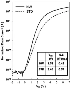
Fig. 3. Typical ID–VGcharacteristics of the STD and the NW SONOS-TFTs. The
parameters of threshold voltage and subthreshold swing are extracted in the insert tables.
implantation was performed with a dose of 5 × 1015cm− 2and the dopant was activated by rapid thermal annealing. Then, a 200-nm TEOS oxide layer was deposited by LPCVD as the passivation layer. Next, the 5 × 5 μm2 contact holes were defined and Al metallization was performed. Finally, the devices were sintered at 400 °C in nitrogen ambient for 30 min.
3. Results and discussion
Fig. 2 shows the TEM photography of a single nanowire channel cross-section. It is clearly observed that the nanowire channel is surrounded by the control gate to form the tri-gate structure. The physical channel width of NW SONOS-TFT is also confirmed 65 nm and the thickness of O/N/O are 5 nm/ 10 nm/10 nm, respectively.Fig. 3presents the normalized ID–
VGcurves of the STD and the proposed NW SONOS-TFTs. The
electrical parameters are also extracted in the insert tables. Comparing the STD device, the NW device has superior electrical performance, such as the higher on-current, smaller threshold voltage (Vth) and subthreshold swing (S.S). Due to the
increase of the effective channel width and the enhancement of the control of the channel region by the tri-gate structure, the drive current and Vth can be improved in NW SONOS-TFT.
Additionally, the drain current at the corner region turns on earlier than that at the surface of the channel due to the crowding of the gate fringing field at the corner edges[13], the additional corner current can increase the drain current as the corner numbers increasing. Therefore, the pronounced enhancement of device with the NW structure is attributed mainly to the good gate control by the tri-gate structure and the larger electrical field induced by its corner effect.
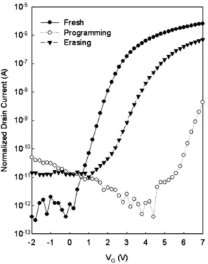
In addition, the SONOS-TFT also can be used as a nonvolatile memory device under adequate gate voltage operation. In this work, the SONOS-TFT memories are programmed and erased by tunneling mechanism.Fig. 4presents the ID–VGcurves of device
before memory operation (Fresh) and after the programming/ erasing operations. During programming operation, electrons
Fig. 5. Self-convergent characteristic of NW SONOS-TFT with a−20 Verasing bias.
Fig. 6. (a) Programming characteristics, and (b) erasing characteristics of memory devices for NW and standard structures.
Fig. 4. The ID–VGcurves of device before memory operation (Fresh) and after
injection form inverted substrate into the nitride layer and be captured by the traps in the nitride layer to increase Vth. If the
programming time is long enough, the Vthwill saturate, and the
saturated Vth value is bias-dependent [14]. Oppositely, during
erasing operation, the captured electrons inject back to substrate form the nitride layer. However, the erased Vthwill also saturate,
and the saturated Vthvalue is determined by the charge balance
between the gate injection into the ONO layer and the de-trapping out of the ONO layer[15]. Therefore, when the SONOS-TFT is functioned as a nonvolatile memory, it has a new reset state threshold voltage different from that in fresh device.
In order to demonstrate the reset state threshold voltage caused by dynamic balance of gate injection and electron de-trapping, the fresh device was erased with a negative bias without any programming operation. As shown inFig. 5, the threshold voltage rises as the erasing time increases and saturates in the end. Com-paring the erasing characteristic of a programmed device with the same negative bias, it is observed that the saturated threshold voltages are self-convergent. Hence, the self-convergent property should be considered as the SONOS-TFT is functioned as a memory device.
Fig. 6(a) and (b) shows the programming and erasing characteristics of NW and standard devices. It can be seen that the memory device with multiple nanowire channels has the superior program/erase (P/E) efficiency and larger memory window shift than STD device. Especially, for the erasing characteristic, it shows that the erasing speed is very slow and the memory window is neatly no shift even at a gate voltage of −12 V in the standard device. The memory characteristics for NW SONOS-TFT improved because the corner effect induced large electrical field at the corners can greatly enhance the programming and erasing performance. Therefore, the P/E efficiency is really improved by the multiple nanowire channels structure.
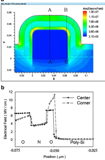
To verify the hypothesis, we performed the simulations of electrical field for single nanowire by ISE-TCAD simulator.
Fig. 7(a) presents the contour plot of electrical field with a gate bias of 14 V. The 2-D simulation shows that maximum electrical field is concentrated near the corners obviously.Fig. 7(b) illus-trates the electrical fields along the AA′ (center) and BB′ (corner) direction, receptively. It can be found that the maximum electrical
Fig. 7. Simulation results of (a) the electrical field contour plot of the nanowire with a gate bias of 14 V, and (b) the electrical fields in ONO gate dielectric at center and corner regions.
Fig. 8. Endurance characteristic of the NW SONOS-TFT. Memory window remains 0.8v after 105P/E cycles without much degradation.
Fig. 9. Data retention characteristics of STD and NW devices at 80 °C. Memory window of both devices are not closure after 10 years.
field is about 11 MV/cm at the corner and 7.5 MV/cm at the center near the SiO2/poly-Si interface. Thus the tunneling current
through the tunneling oxide is larger at the corners than at the center of nanowire. Similarly, the erasing characteristic also can be improved by the corner effect induced large electrical field during erasing operation. Therefore, the pronounced enhance-ment of device with the NW structure is attributed to the large number of corners and their corner effect.
Fig. 8shows the retention characteristics for NW and standard SONOS-TFTs at 80 °C. The devices are programmed and then measured at raised temperature. The results indicate that both devices exhibit large memory windows and neatly no degradation at a 10-year retention time tested at 80 °C. The endurance characteristic of NW SONOS-TFT with 12 V 10 ms and−14 V 1.5 s stress is shown inFig. 9. It can be seen that the programmed/ erased threshold voltage both increase as the number of cycles increases at the beginning and saturates to retain a constant memory window. The increase in threshold voltages could be due to the programming and erasing efficiencies are not compatible. However, the memory window is not closure obviously and the memory window can remain a 0.8 V after 5 × 10³P/E cycles. 4. Conclusions
A novel poly-Si TFT combined with nonvolatile SONOS memory and nanowire structure is demonstrated in this study. The SONOS-TFT can be functioned as a transistor or a nonvolatile memory at the same time. Due to the tri-gate structure and additional corner current induced by corner effect, the NW SONOS-TFT has the superior electrical characteristics than a standard device. Under an adequate gate bias operations, the proposed device exhibits superior memory characteristics with high program/erase efficiency. The simulation of electrical field results verified that the enhancement of P/E efficiency in NW SONOS-TFT is mainly attributed to the large number of corners and their corner effect. In addition, the good retention and endurance are also obtained in this device. The fabrication of SONOS-TFTs with nanowire channels is quite easy and involves
no additional processes. Such a SONOS-TFT is very promising to be used for application in the future system-on-panel display. Acknowledgment
This work was performed at the National Nano Device Laboratory and was supported by the National Science Council of the Republic of China under Contract Nos. NSC-96-2120-M-110-001. Also, this work was partially supported by the MOEA Technology Development for Academia Project # 95-EC-17-A-07-S1-046 and MOE ATU Program #95W803.
Reference
[1] S.D.S. Malhi, H. Shichijo, S.K. Banerjee, R. Sundaresan, M. Elahy, G.P. Polack, W.F. Richardson, A.H. Shah, L.R. Hite, R.H. Womack, P.K. Chatterjee, H.W. Lam, IEEE Trans. Electron Devices 32 (1985) 258. [2] T. Yamanaka, T. Hashimoto, N. Hasegawa, T. Tanaka, N. Hashimoto, A.
Shimizu, N. Ohki, K. Ishibashi, K. Sasaki, T. Nishida, T. Mine, E. Takeda, T. Nagano, IEEE Trans. Electron Devices 42 (1995) 1305.
[3] M. Aoki, T. Hashimoto, T. Yamanaka, T. Nagano, Jpn. J. Appl. Phys. 35 (1996) 838.
[4] T. Aoyama, K. Ogawa, Y. Mochizuki, N. Konishi, IEEE Trans. Electron Devices 43 (1996) 701.
[5] K. Yoneda, R. Yokoyama, T. Yamada, Proc. Symp. VLSI Circuits, 2001, p. 85. [6] H. Tokioka, M. Agari, M. Inoue, T. Yamamoto, H. Murai, H. Nagata, Proc.
SID, 2001, p. 280.
[7] K.H. Wu, H.C. Chien, C.C. Chan, T.S. Chen, C.H. Kao, IEEE Trans. Electron Devices 52 (2005) 987.
[8] X. Wang, D.L. Kwong, IEEE Trans. Electron Devices 53 (2006) 78. [9] Y.H. Lin, C.H. Chien, T.H. Chou, T.S. Chao, C.Y. Chang, T.F. Lei, IEDM
Tech. Dig., 2005.
[10] S.I. Hsieh, H.T. Chen, Y.C. Chen, C.L. Chen, Y.C. King, IEEE Electron Device Lett. 27 (2006) 272.
[11] Y.C. Wu, T.C. Chang, P.T. Liu, C.S. Chen, C.H. Tu, H.S. Zan, Y.H. Tai, C.Y. Chang, IEEE Trans. Electron Devices 52 (2005) 2343.
[12] G. Fiori, G. Iannaccone, G. Molas, B.D. Salvo, IEEE Trans. Nanotechnol. 4 (2005) 326.
[13] B. Doyle, B. Boyanov, S. Datta, M. Doczy, S. Hareland, B. Jin, J. Kavalieros, T. Linton, R. Rios, R. Chau, Proc. VLSI Tech. Symp., 2003, p. 133. [14] S. Manzini, J. Appl. Phys. 62 (8) (1987) 3278.
[15] Y.H. Shih, H.T. Lue, K.Y. Hsieh, R. Liu, C.Y. Lu, IEDM Tech. Dig., 2005, p. 881.