Adjusting optical resonance thickness to increase the conversion efficiency of
polymer solar cells
Yu Sheng Tsai
a, Jian-Shian Lin
b,c, Wei-Ping Chu
a, Po-Hsun Wang
a, Fuh-Shyang Juang
a,*, Ming-Hua Chung
d,
Chin-Ming Chen
d, Mark O. Liu
ea
Institute of Electro-Optical and Materials Science, National Formosa University, Huwei, Yunlin 63208, Taiwan, ROC
bDepartment of Mechanical Engineering, Osaka University, Osaka, Japan Yamadaoka 2-1, Suita, Osaka 565-0871, Japan c
Mechanical and System Research Laboratories, Industrial Technology Research Institute, HsinChu, Taiwan 310, ROC
d
Department of Material Science and Engineering, National Chiao Tung University, Hsinchu, Taiwan 30010, ROC
e
Material and Chemical Research Laboratories, Industrial Technology Research Institute, Hsinchu, Taiwan 300, ROC
a r t i c l e
i n f o
Article history:
Received 2 November 2009
Received in revised form 1 February 2010 Accepted 16 February 2010
Available online 6 March 2010 Keywords: P3HT PCBM Polymer Solar cells Optical resonance
a b s t r a c t
The derivatives of C60, [6,6]-phenyl C61-butyric acid methyl ester (PCBM), and 3-hexylthiophene (P3HT)
were dissolved in DCB solvent, then spin coated into an active layer for polymer solar cells. The experi-mental parameters were studied carefully to obtain the optimum power conversion efficiency (PCE). The primary process for generation of photocurrent in an organic photovoltaic device is the generation of bound electron–hole pairs (excitons) by absorption of energy (photons) from the optical electric field. Modeling was based on the assumption that the photocurrent generation process is the result of the cre-ation and diffusion of photogenerated species (excitons), which are dissociated by charge transfer at the active layer. Improve organic optics absorb by insert organic layer (CuPc or C60) at the active layer/Al
interface. This research is divided into two components. First part, we use n-type C60as transmission
layer. When an optimum thickness of C60is 5 nm, the Jscof polymer solar cell can be increased from
7.26 mA/cm2to 7.7 mA/cm2. The V
ocdecrease is because the energy level of C60LUMO (lowest
unoccu-pied molecular orbital) at 4.5 eV is higher than the 3.7 eV of PCBM. Second part, we use p-type CuPc as transmission layer. When an optimum thickness of CuPc is 3 nm, the short circuit photo-current den-sity (Jsc) and open circuit voltage (Voc) of polymer solar cell can be increased from 7.26 mA/cm2to 8.0 mA/
cm2and 0.56–0.58 V, respectively. The reason is the same as C
60. The Vocincrease is because the energy
level of CuPc LUMO (lowest unoccupied molecular orbital) at 3.1 eV is lower than the 3.7 eV of PCBM. The Jscincrease is because the 3 nm of CuPc leads to a constructive interference happened in the active layer
and thus optical absorption increases. In this study we used 3 nm of CuPc at the active layer/Al interface to enhance the short circuit current density, and the efficiency was increased to 2.94%.
Ó 2010 Elsevier B.V. All rights reserved.
1. Introduction
Poly(3-hexylthiophene) (P3HT) has an excellent nature of film formation and possesses good semiconductor properties. For example its containing a higher carrier mobility rate and therefore can be applied on the production of optoelectronic devices for flex-ible plastic substrates. In 1995 Heeger et al. used a mixture of MEH-PPV and PCBM to form a single-layer heterogeneous struc-ture, in which PCE reached 1.5%[1]. In 2001 Sariciftci et al. used a mixture of MDMO-PPV and PCBM, and also LiF/Al as the cathode to improve the efficiency to 2.1%[2]. In 2005 Yang et al. took use of the self-organization effect and with slow growth treatment to re-duce the resistance of devices connected in series resistance, which enhanced the carrier mobility rate and increased the efficiency to
4.37%[3]. In the same year Heeger et al. produced devices which PCE reached 5%[4]. It was done mainly by the use of P3HT/PCBM [poly(3-hexylthiophene)/[6,6]-phenyl C61-butyric acid methyl es-ter] to create P–N junction structures for solar cell devices[5,6]. In 2008, Chunfu Zhang et al. inserted the donor material, CuPc, be-tween the active layer and anode. They demonstrated a simple tan-dem structure of organic photovoltaic cells for efficient light harvesting[7]. Because organic solar cells have the advantages of low cost, lightweight, deflectable, and can easily produce for large areas[8–10], they are in worth for further research. In this study, we reports effects of organic solar cells with difference organic material (C60or CuPc) and optical resonance thickness.
2. Experimental
The sheet resistance and thickness of the ITO glass substrate were 5X/h and 280 nm respectively. Photo-lithography was used
1567-1739/$ - see front matter Ó 2010 Elsevier B.V. All rights reserved. doi:10.1016/j.cap.2010.02.015
*Corresponding author. Tel.: +886 5 631 5600; fax: +886 5 631 5604. E-mail address:[email protected](F.-S. Juang).
Current Applied Physics 10 (2010) S502–S505
Contents lists available atScienceDirect
Current Applied Physics
to define the anode plot. The glass substrate was then placed with-in an ultrasound washer, with-in sequence uswith-ing acetone, methyl alco-hol and deionized water (DI water) each for 8 min. The glass substrate was then blown dry by nitrogen and placed in an oven for 30 min. The substrate was then placed within a oxygen plasma washing machine. The surface of the ITO glass was cleaned in an oxygen plasma environment of oxygen flow rate 10 sccm, RF power 30 W. The substrate was then removed and spin coated a layer of PEDOT:PSS to repair the ITO surface to assist the holes transfer to the electrode. The substrate was then removed and placed in a N2 glove box. The active layer material
(P3HT:PCBM = 1:1, 1.7 wt%) was then dissolved in o-dichloroben-zene (DCB) and placed on a hot-plate at temperature 40 °C, rota-tion speed 150 rpm for 24 h. The P3HT:PCBM solurota-tion was then spin coated on the PEDOT:PSS layer. After the coating of the organ-ic layer, the devorgan-ice was placed within a Petri dish of diameter 12.9 cm and height 4.5 cm. A vapor chamber was formed by plac-ing the device and solution on a hot-plate, and covered with a Petri dish. Total growth time was 40 min. By slow growth treatment the active layer had a self-organization effect. Because the device was placed within a saturated vapor environment, thus no film forma-tion will occur on the active layer and still in a soluforma-tion state. By the self-organization effect P3HT and PCBM will self-organized. Sample placed on a hot-plate before annealing prior to organic layer evaporation, and placed within an organic evaporation to ap-ply evaporated C60or CuPc, to increase the short circuit
photo-cur-rent density of the polymer solar cells. By vaporization for metal deposition LiF/Al was used as the cathode. The device area size is 0.04 cm2. After the completion of device production, AM 1.5G 100 mW/cm2was used as sunlight simulation. A KEITHLEY 2400
was used for measuring the current–voltage characteristics of the polymer solar cells. The IPCE spectra were recorded by illuminating the sample with 100 W halogen lamp by PV measurement corpora-tion (USA).
3. Results and discussion
3.1. Comparison of different optical resonance thickness of C60
The inserting of the accepting material, C60, between the active
layer and cathode was to mainly change the C60thickness, allowing
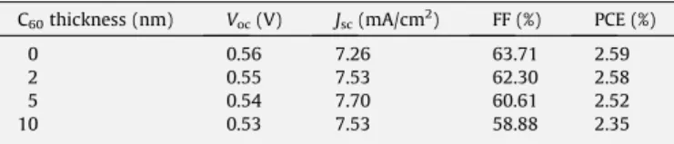
the optical resonance region lie between the active layer and the thin film, allowing the short circuit photo-current density and effi-ciency increase.Table 1andFig. 1are the characteristic curves and J–V curve plots for a device vaporization-coated with C60
thick-nesses of 0 nm, 2 nm, 5 nm and 10 nm, respectively. When the C60 thickness increased to 2 nm, the short circuit photo-current
density of the device increased from 7.26 to 7.53 mA/cm2. From
the literatures[11–13], it is known that the incident light optical resonance region would move between the active layer and thin film thickness. When C60thickness increased to 5 nm, the incident
light optical resonance region would create the maximum short circuit photo-current density for the device of 7.70 mA/cm2
be-tween the thin film thickness of the active layer. As C60thickness
increased to 10 nm, the optical resonance region would deviate from the active layer thin film, and caused the short circuit
photo-current density of the device reduce to 7.53 mA/cm2. In addition, the open circuit voltage was found to decrease as the C60thickness increased. The reason was because the open circuit
voltage of the device was determined by the energy gap of HOMODoner–LUMOAccept[14]. From the energy gap plot for solar
cells in Fig. 2, it could be seen that the energy gap for HOMODoner–LUMOAccept before any vaporization-coating of C60
was 1 eV; once C60was introduced, since the LUMO of C60is higher
than its PCBM, the energy gap of HOMODoner–LUMOAcceptdecreased
to 0.8 eV, and thus the energy gap for HOMODoner–LUMOAccept
reduced 0.2 eV, and causing the open circuit voltage of the device to drop. The curve fill-factor also decreased as the C60thickness
in-creased. There were two main reasons for this phenomenon: first, the total thickness of the device increased, which caused the series resistance to increase and thus the curve fill-factor to slightly de-crease. The second reason was that the created excitons as the polymer solar cell receives sunlight from distributed from the ac-tive layer in all directions. When the excitons distributed to the do-nor–acceptor interface, the existing inside electric field would cause the excitons separate into electrons and electron holes. Valid currents are generated by collecting with electrodes. However, as the excitons move to the interface of the active layer and C60, since
the LUMO of C60when compared with the active layer is higher, it
would cause the excitons move to the C60layer, and resulting with
the loss of the excitons. This causes current leakage of the solar cell, and reduced the curve fill-factor of the device. When the vaporization-coating of C60was 2 nm, the device obtained the
opti-mal characteristics: the open circuit voltage was 0.55 V, the short circuit photo-current density was, 7.53 mA/cm2, the curve
fill-fac-tor was 62.30%, and the efficiency was 2.58%.
3.2. Comparison of different optical resonance thickness of CuPc Since C60 material would cause the open circuit voltage and
curve fill-factor of the device to decrease, and causing the device’s
Table 1
Device characteristics with different thicknesses of C60.
C60thickness (nm) Voc(V) Jsc(mA/cm2) FF (%) PCE (%)
0 0.56 7.26 63.71 2.59 2 0.55 7.53 62.30 2.58 5 0.54 7.70 60.61 2.52 10 0.53 7.53 58.88 2.35 -0.1 0.0 0.1 0.2 0.3 0.4 0.5 0.6 -8 -7 -6 -5 -4 -3 -2 -1 0 1
Current Density (mA/cm
2 )
Voltage (V) Active layer/C60(x nm)/Al
without 2 nm 5 nm 10 nm
Fig. 1. J–V curve plots with different thicknesses of C60.
PEDOT :PSS 5.0 eV 3.5 eV 3.3 eV 4.3 eV 5.3 eV 6.0 eV P3HT PCBM C60 4.5 eV 6.2 eV ITO 4.7 eV Al 4.2 eV LiF For h+transport For e-transport For h+transport For e-transport
Fig. 2. Energy gap between the active layer and cathode with the coating of C60.
efficiency unable to rise, therefore CuPc was used to replacing the coating between the active layer and cathode. As the LUMO of CuPc is higher than C60, the current leakage of the device was reduced
and the open circuit voltage increased, which increased the effi-ciency of the polymer solar cell.Table 2andFig. 3are the charac-teristic curves and J–V curve plots for a device vaporization-coated with CuPc thicknesses of 1 nm, 3 nm and 6 nm respectively. When the CuPc thickness was 1 nm, the incident light optical resonant maximum was adjusted and shifted into the active layer. But due to the LUMO of CuPc is lower than that of PCBM as shown in
Fig. 4, the electrons need to jump over a barrier in order to be transported to the cathode. Therefore, the short circuit current density of the device with 1 nm CuPc decreased to 6.49 mA/cm2. When the CuPc thickness increased to 3 nm, the incident light res-onant maximum was just located in the central region of active layer which resulted in a maximum short circuit current density of 8.00 mA/cm2. When the CuPc thickness increased to thicker than
3 nm, the photo-induced electrons were more difficult to be trans-ported to the cathode and the incident light optical resonant maximum may deviate from the center region in the active layer. Therefore the device with 5 nm CuPc has lower short circuit current density than that with 3 nm CuPc. In addition, with the increasing of the vaporized CuPc thickness, the open circuit voltage of the device was determined by the gap energy of HOMODoner–LUMOAccept. From the energy gap plot for solar cells
in Fig. 3, it could be seen that the original energy gap for HOMODoner–LUMOAccept before any vaporization-coating of CuPc
was 1 eV; once CuPc was introduced, since the LUMO of CuPc is lower than its PCBM, the energy gap for HOMODoner–LUMOAccept
in-creased to 1.8 eV, and thus the open circuit voltage of the device increased (seeFig. 4). The curve fill-factor also slightly decreased as the CuPc thickness increased. The main reason was the total thickness of the device caused the series resistance to increase and thus the curve fill-factor to slightly decrease.Fig. 5displays the IPCE results of photovoltaic cells fabricated with difference or-ganic material. The IPCE maximum of 42.7% at 510 nm was ob-served for ITO/PEDOT:PSS/active layer/LiF/Al. The IPCE of photovoltaic cells was observed to be 48.1% at the same wave-length for ITO/PEDOT:PSS/active layer/C60/LiF/Al, due to the
exci-tons move to the C60 layer, and resulting with the loss of the
excitons. The IPCE of polymer solar cells was increased to 47.3%
at the same wavelength for ITO/PEDOT:PSS/Active layer/CuPc/LiF/ Al, due to two reason: (1) increase in the Incident photon-to-cur-rent conversion efficiency as a result of the optical resonance pres-ent in the active layer, (2) the excitons inability to move to the CuPc layer, resulting in no loss of excitons.Table 3shows the com-parisons of Jsc from I–V curves with those from IPCE
measurements.
When the vaporization-coating of CuPc was 3 nm, the device obtained the optimal characteristics: the open circuit voltage was 0.58 V, the short circuit current density of 8.00 mA/cm2, the curve
fill-factor of 63.36%, and conversion efficiency of 2.94%. 4. Conclusion
In the study, the inserting of an optical resonance thin film be-tween the active layer and cathode could increase the short circuit photo-current density and efficiency of the device. In addition, the LUMO of the optical resonance thin film may not have a large difference with the difference between PCBM and LUMO; as an over-high LUMO would cause the open circuit voltage and curve fill-factor to decrease, and an over-low LUMO would require the created electrons of the polymer solar cell device to jump over a
Table 2
Device characteristics with different thicknesses of CuPc.
CuPc thickness (nm) Voc(V) Jsc(mA/cm2) FF (%) PCE (%)
0 0.56 7.26 63.71 2.59 1 0.57 6.49 63.53 2.35 3 0.58 8.00 63.36 2.94 6 0.58 7.22 62.80 2.63 -0.1 0.0 0.1 0.2 0.3 0.4 0.5 0.6 -8 -7 -6 -5 -4 -3 -2 -1 0 1
Current Density (mA/cm
2 )
Voltage (V) Active layer/CuPc(x nm)/Al
without 1 nm 3 nm 6 nm
Fig. 3. J–V curve plots with different thicknesses of CuPc.
PEDOT :PSS 5.0 eV 3.5 eV 3.3 eV 4.3 eV 5.3 eV 6.0 eV P3HT PCBM 3.5 eV 5.2 eV CuPc ITO 4.7 eV Al 4.2 eV LiF For h+transport For e-transport For h+transport For e-transport
Fig. 4. Energy gap between the active layer and cathode with the coating of CuPc.
400 450 500 550 600 650 700 0 10 20 30 40 50 IPCE (%) Wavelength (nm) Without C60-2nm CuPc-3nm
Fig. 5. Incident photon-to-current conversion efficiency (IPCE) curves for the optical resonance material photovoltaic cells fabricated.
Table 3
The comparisons of Jscfrom I–V curves with those from IPCE measurements.
Jscof I–V(mA/cm2) Jscof IPCE (mA/cm2)
Without 7.26 5.40
C60-2nm 7.53 6.08
CuPc-3nm 8.00 6.16
barrier to reach the cathode. When an optimum thickness of CuPc is 3 nm was chose, the short current (Jsc), open voltage (Voc) and
power conversion efficiency (PCE) of a polymer solar cell can be increased from 7.26 mA/cm2 to 8.00 mA/cm2, and 0.56–0.58 V,
and 2.58–2.94%, respectively.
Acknowledgements
This project was supported by the National Science Council for the funding of this project No. NSC 97-2221-E-150-007. The IPCE measurement was supported by the National Nano Device Laboratory. The authors appreciate Mr. Yuan-Fu Tang, Mr. Hsiang-Sheng Wen and Teh-Chao Liao’s kind help in the device measurement.
References
[1] G. Yu et al., Science 270 (1995) 1789.
[2] S.E. Shaheen et al., Applied Physics Letters 78 (2001) 841. [3] G. Li et al., Nature Materials 4 (2005) 864.
[4] W. Ma et al., Advanced Functional Materials 15 (2005) 1617. [5] T. Yamanari et al., IEEE 1 (2006) 240.
[6] A.J. Chatten et al., IEEE 1 (2005) 31.
[7] Chunfu Zhang, Shi Wun Tong, Changyun Jiang, E.T. Kang, D.S.H. Chan, Chunxiang Zhu, Applied Physics Letters 92 (2008) 083310.
[8] H.J. Lee et al., IEEE 1 (2006) 233.
[9] M. Al-Ibrahima et al., Solar Energy Materials and Solar Cells 85 (2005) 13. [10] S.H. Jin et al., Solar Energy Materials and Solar Cells 91 (2007) 1187. [11] Alan J. Heeger et al., Advanced Materials 18 (2006) 789–794.
[12] L.A.A. Pettersson, L.S. Roman, O. Inganäs, Journal of Applied Physics 86 (1999) 487.
[13] T. Stübinger, W. Brütting, Journal of Applied Physics 90 (2001) 3632. [14] H. Hänsel et al., Advanced Materials 15 (2003) 2056.