Averaging and Cancellation Effect of High-Order
Nonlinearity of a Power Amplifier
Chien-Ping Lee, Fellow, IEEE, Wenlong Ma, and Nanlei Larry Wang
Abstract—Nonlinear distortion of a power amplifier (PA) due to the nonlinear input-output transfer function is studied. The high-order nonlinearity or Fourier components of the output, due to the mixing of input signals, are found to be related to an average integral related to the transfer function, thus giving insight to the cancellation effect of the nonlinearity. A simple formula has been derived to relate the th-order Fourier component of a nonlinear transfer function with a sinusoidal input to an average integral of the th-order derivative of the transfer function. The large signal nonlinear distortion of the th-order can therefore be regarded as a weighted average of the th-order derivative of the transfer function. For PAs, the averaging effect gives rise to local minima in the intermodulation distortion terms during power sweep because of the cancellation of the positive part and the negative part of the derivative during averaging. We have applied the formula to InGaP heterojunction bipolar transistors PAs and are able to explain most of the observed nonlinear phenomena of the amplifiers.
Index Terms—Fourier transforms, heterojunction bipolar tran-sistors (HBT), intermodulation distortion (IMD), nonlinear distor-tion, power amplifiers (PAs).
I. INTRODUCTION
N
ONLINEAR distortion plays a crucial role in the perfor-mance of a power amplifier (PA). For modern communica-tion systems, nonlinear mixing of different carrier frequencies gives rise to undesirable sidebands that are difficult to be filtered out. High-order nonlinearity, however, depends on many factors including the device characteristics, the circuit design, the op-eration environment, etc., making it very difficult to understand analytically [1], [2].Traditional ways using Volterra series together with Taylor expansion provides a simple means to understand the small-signal intermodulation distortion (IMD) and the weakly nonlinear behavior of a device. But it loses its validity at large signal operations. To know the large signal behavior, one is usually forced to use circuit simulations, where true phys-ical meanings are often lost in the complicated calculations. Some have developed computational techniques and approxi-mation schemes to tackle this large signal nonlinear problem [3]–[6]. Others have tried to understand it phenomenologically, usually through small-signal expansion and circuit simulations
Manuscript received August 26, 2006; revised January 22, 2007, and April 18, 2007. This paper was recommended by Associate Editor B. C. Levy.
C.-P. Lee is with W J Communications, Inc., San Jose, CA 95134 USA and also with the Department of Electronics Engineering, National Chiao Tung Uni-versity, Hsin Chu, Taiwan 30010, R.O.C. (e-mail: [email protected]).
W. Ma is with W J Communications, Inc., San Jose, CA 95134 USA. N. L. Wang was with W J Communications, Inc., San Jose, CA 95134 USA. He is now with Palm, Inc., San Jose, CA 94085 USA.
Digital Object Identifier 10.1109/TCSI.2007.905650
[7]–[14]. Although many nonlinear behaviors of various de-vices can be explained successfully, a good physically based mathematical model is lacking.
One of the most interesting and puzzling things in the high-order IMD behavior is the local minima or dips in the power sweeps of the IMD curves. Previous work has tried to link this phenomenon with small-signal sweet spot and/or some other cancellation effects [11], [15]–[23]. However, a sound physical understanding is still needed.
While the small-signal sweet spots are well defined by the zero points of the third derivative of the output transfer function with respect to the input, the dips, or the large signal sweet spots have not been clearly defined mathematically. In this work, we try to provide a mathematical foundation for this large signal phenomenon. A simple formula was derived based on first prin-ciple Fourier analysis. It relates the th-order nonlinearity to an average integral of the th derivative of the output transfer function. The theoretical analysis given in this paper deals di-rectly with the nonlinear – transfer function of a device. The more complicated reactant components which give rise to non-linear dynamic effects are not considered. Although the analysis represents an idealized situation, it provides insight and under-standing to the behavior of large signal nonlinearity of the de-vice. The result explains clearly the cancellation or averaging effect in the IMD behavior.
II. FOURIERCOMPONENTS ANDAVERAGEINTEGRAL
To make the problem simple, we assume in the following analysis that the nonlinearity comes from a memoryless non-linear transfer function, i.e., an – relationship :
(1) Under harmonic modulation
(2)
where and . For a single tone input, the
th-order harmonic of the output is simply the th-order Fourier component
(3)
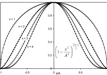
Fig. 1. Weighting functions for the first four harmonic distortion terms. Notice the curve gets narrower as the order of the distortion is higher.
Here HD stands for harmonic distortion. However, it is often difficult to visualize this equation through the integration in the time domain. Since all the information is in the transfer function itself, it is easier to look at the property of the function with the input voltage as the variable. We have derived a very interesting formula, which relates each harmonic term with an average in-tegral with respect to the input voltage. Letting the modulation signal , we can show that (3) is equivalent to (see Appendix A)
(4) The integration is now performed in the domain of the input voltage. We can see that the th-order harmonic is simply an average of the th-order derivative of the transfer func-tion over the input voltage swing with a weighting funcfunc-tion, . It is noticed that this weighting function is symmetrical and centered at the bias point . This property is important because the averaging would not be meaningful if the weighting function is not well behaved. Fig. 1 shows the weighting function for the first four harmonics. We can see that the maximum of the function is at the bias point, , and because of the shape of this function, the center portion of the voltage swing is more important than the edge when the average integration is performed using (4). For higher order harmonics, the weighting function becomes narrower, so the effective average range also becomes smaller.
When the input has two tones, i.e.,
, the nonlinear response of the transfer function gives
(6)
Similar to (4), by letting and , we
can also prove that this integral is the same as shown in (7) at the bottom of the page. The intermodulation component of the ’s order is still an average of the transfer function’s th-order derivative, but it is done in two dimensions. So for large signal modulations, no matter whether it is single tone or multi-tones, we can visualize the nonlinear distortion by looking at the weighted average of certain derivative of the transfer function in the range of the voltage swing.
III. THIRDHARMONICDISTORTION ANDIMD DISTORTION
Now let’s focus on the third-order IMD with two-tone exci-tation. Equation (7) becomes
(8) The average is taken for the third derivative of the transfer func-tion, which is the same as the third-order harmonic for a single tone input. In the small-signal limit, the derivative term can be taken out from the integral and (8) reduces to
(9) This result is the same as that obtained by Volterra expansion using Taylor series. For single tone input, the third-order har-monic distortion, according to (4), is
(10)
Fig. 2. Transfer function and its third derivative as functions ofV . (the transfer function is theI–V of an HBT curve along a load line).
At the small-signal limit, it reduces to
(11) Comparing (9) with (11), we find there is a factor of three difference between the two. At the same input power, however, these two values are about the same because the voltage swing, , for two tone input shown in (9) is times that of the swing for a single tone input in (11). At large signals, because the weighting functions are different, the single tone will be different from the two-tone IMD3. However, because both nonlinear distortions ((8) and (10)) are based on some kind of averaging effect of the third-order derivative of the transfer func-tion, the physics of the two is basically the same.
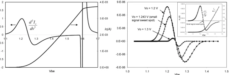
For simplicity, we use shown in (10) to illustrate the averaging effect of the third-order nonlinear distortion in the following. InGaP/GaAs HBT PAs are used here as examples. These amplifiers are designed for high power and high linearity applications [25]. By examining the third derivative of the – relationship, we know that the nonlinearity of a bipolar tran-sistor mainly comes from two parts of the – curve. One is from where the device is turned on, the other is from where the device reaches saturation [7]. Fig. 2 shows the transfer function and its third derivative of an InGaP HBT when the device op-erates along a certain load line. The emitter size of the device is 24 m and the emitter resistance, which includes a ballast resistor, is 80 . From the exponential – relationship of a bipolar transistor (before saturation)
(12) the third derivative is
(13) where . This function goes to zero when the cur-rent is both very low and very high, and is significant when is close to . It goes from positive to negative when
Fig. 3. Integrand of (10) for an input voltage swing of 0.1 V at several bias voltages.V o = 1:2 V is below, 1.3 V above and 1.243 V at the small-signal sweet spot.
crosses . This zero crossing point corresponds to the small-signal IMD sweet spot according to (9) and (11). This point also corresponds approximately to the point where the de-vice is turned on.
Because the third derivative of the transfer function can be either positive or negative, the average integrals shown in (8) and (10) give a cancellation effect as the voltage swings across the positive and the negative regions. To illustrate such effect, we show in Fig. 3 the integrand of (10) for a voltage swing of
V at several different bias voltages. The collector current and its third derivative are shown in the inset. When the bias point (at 1.2 V) is below the small-signal sweet spot, the positive portion of the integrand is larger than the negative portion, so the net integral yields some HD or IMD with a positive sign. When the bias point (at 1.3 V) is above the sweet spot, the negative portion is larger than the positive portion. The integral in (10) gives a net negative value, also contributing to HD or IMD. When the bias point is at the sweet spot, V, the positive part of the integrand is close to the negative part. So the resulting integral becomes very small and it results in a very small HD or IMD value. It should be noticed, because the third derivative of the current is not symmetrical with respect to the sweet spot, the cancellation effect would not be very good if the voltage swing is large. In other words, the small-signal sweet spot does not corresponds to a null IMD or HD for large signal operations.
Let’s now pick a bias point above the small-signal sweet spot but not too much away, say V, corresponding to a typical class AB operation. The integrands of (10) at different voltage swings are shown in Fig. 4. When the voltage swing is small ( V, 0.1 V), the negative part of the integrand is larger than the positive part. When the voltage swing is large ( V), the positive part becomes dominant. When the swing is at 0.2 V, the area of the positive portion is close to that of the negative portion. So the average integral of (10) gives rise to a dip in the third-order distortion in a power sweep.
The output of the fundamental frequency can be also calcu-lated using (4) by taking the first-order term, i.e., . In this way most of the characteristics of the amplifier can be cal-culated. Fig. 5 shows the calculated and the component
Fig. 4. Integrand of (10) atV o = 1:26 V but with different input voltage swings.
Fig. 5. Calculated fundamental output and the third-order harmonic distortion versus input power atV o = 1:26 V. Several input voltage swings are marked on the curve.
for the fundamental frequency (FD) versus the input power at a bias V. A clear dip in this distortion curve is clearly seen. The four points corresponding to the four different input voltage swings shown in Fig. 4 are marked on the curve. The dip position corresponds to approximately an input swing of 0.2 V, which is the input swing that gives a very small average integral mentioned above.
It is also noticed that besides the dip caused by the device turn-on, there is another dip, which is much sharper and nar-rower, at high power levels. This is due to the large swing in the third derivative when the device is close to saturation (see Fig. 2). We can show from (10) that at the limit of very large voltage swing, the ratio of (FD being the fundamental frequency amplitude) tends to an asymptotic value of (see Appendix B). This is the same as what Pedro has derived [7]. There is a 180 phase difference between the term and the FD term. So for any input power level that gives a positive av-erage integral, there will be a dip in the distortion curve before the device goes to saturation, because it has to go negative at full saturation.
The behavior of the third-order distortion versus power de-pends on the bias point very much. If the bias point is at or below the small-signal sweet spot, corresponding to class B or class C
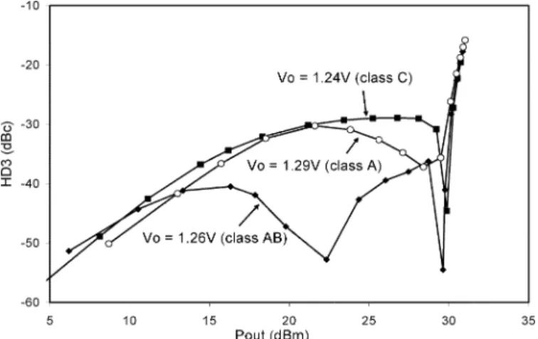
Fig. 6. Calculated third-order harmonic distortion versus the output power of the fundamental frequency.V o =1.24, 1.26, and 1.29 V.
Fig. 7. Calculated third-order harmonic distortion versus the output power of the fundamental frequency.V o =1.25, 1.26, and 1.27 V.
operation, the average integral will always be positive before saturation (see Fig. 3). In these situations, the dip at low powers will no longer be visible. On the other hand, if the bias point moves way above the small-signal sweet spot, high class AB or class A operations, the average integral will always be negative as power increases. In this case, not only the first dip disappears, the second dip at high powers also becomes not clear. When is biased with a value slightly higher than the small-signal sweet spot, a dip associated with the device turn-on at mid power levels appears. In this situation, one can take advantage of the distor-tion dip to design a high linearity amplifier. The effect of the bias point on the overall third-order linearity is shown in Fig. 6, where the third-order distortion is shown as a function of output power. Three bias points corresponding to the three situations described above were chosen to show the effect.
For class AB amplifiers, where most PAs operate, the dip position can be changed by the bias point. It moves to higher power levels as the bias increases. This effect is shown in Fig. 7. We have compared the experimentally measured results with the calculated results based on the simple formula pre-sented in this paper. Fig. 8(a) shows the measured IMD3 as a function of output power (at 2.14 GHz) of a PA based on the 28 V InGaP/GaAs HBT technology [25]. The power sweep
Fig. 8. (a) Measured IMD3 of a 28 V InGaP/GaAs HBT PA at different quies-cent currents. (b) Calculated curves based on the formula presented in this work.
was made for four different quiescent currents. The quiescent current is directly related to the Vbe bias point, which is used in the calculation. The corresponding calculated curves are shown in Fig. 8(b). It should be mentioned that the calculation was based on an ideal bipolar transfer function and the simple formula presented in this paper. Very reasonable agreement was obtained. The reason that the measured curves show sharper and deeper dips than those in the measured curves is due to the device’s reactant components, which tend to damp out the sharp dips and are not considered in our formula.
The cancellation of IMD described above depends on the third derivative of the transfer function. Although an InGaP HBT is used here as an example, the turn on characteristic is similar to those of many other devices. Fager et al. have studied the bias dependent nonlinearity of an LDMOS [26]. Their ex-perimental results on the appearance of the dips and how they change with bias point agree well with what described in Figs. 6 and 7. The qualitative explanation given by [26] also agrees with the theory presented here.
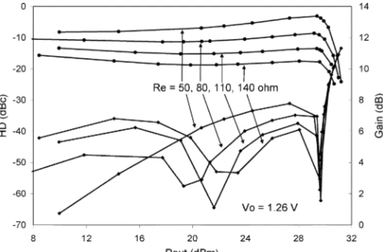
The ideal bias point depends on the emitter resistance because the small-signal sweet spot position is a function of ((13)). A higher requires a lower quiescent bias current or a lower . If we fix the bias point, a higher will in general move the dip to a higher power level. Fig. 9 shows the calculated results for devices with different ’s. We may notice that besides the move of the dip position, the low power nonlinearity is also different for different ’s. Contrary to what one would expect, a high value gives a worse distortion. This is due to the fact that for class AB operation, the small-signal sweet spot moves further away from the bias point (1.26 V in this case) as is increased. So the magnitude of the third derivative seen at the bias point and therefore the nonlinearity are increased when is higher. Notice the gain changes with , so the value cannot be arbitrarily changed.
For two-tone inputs, besides IMD3 corresponding to -other higher odd-order terms can also contribute to distortions close to the fundamental frequency. From (4) and (7), we can see that the averaging effect is different for IMDs with different orders because of the different weighting functions. As men-tioned earlier, the weighting function is narrower for higher
Fig. 9. Effect ofRe on the third-order harmonic distortion. V o is 1.26 V and Re’s are 50, 80, 110, and 140 .
Fig. 10. IMDs corresponding to thirdf2; 01g, fifth f3; 02g, and seventh f4; 03g orders as functions of the input power. The dip position shifts to higher power as the order is higher.
order terms. So the averaging effect will not be as effective as that in the lower order terms. This phenomenon can be seen clearly in Fig. 10, where the output power of the fundamental mode, the third-order mode ( - ), the fifth-order mode ( – and the seventh-order mode ( – ) of a PA are shown as functions of the input power. The simulation was done by harmonic balance and the bias point was chosen for class AB operation. It can be seen that the dip position for the IMD terms shifts to higher power levels as the order of IMD increases. From the average integrals described above, we can see that a larger voltage swing or a higher input power is needed to cancel the positive and the negative parts of the derivative when the IMD order is high. While for lower order terms, because of the wider weighting function, a smaller input
nonlinear device, to understand some of the most important phenomena in the large signal nonlinearity.
IV. CONCLUSION
In conclusion, we have derived a very useful formula, which relates the th-order Fourier component of a transfer function with sinusoidal input to an average integral of the th-order derivative of the transfer function. The average integral is done in the span of the input swing with a symmetrical weighting function that depends on the order of the effect considered. This formula is useful for understanding the cancellation effect of the high-order nonlinear distortion of a nonlinear system under large signal operations. It is particularly useful for under-standing the dip of the IMDs of PAs. Using an InGaP HBT PA as an example, we have successfully explained how the IMD dips change with the bias point and the emitter resistance.
APPENDIXA Derivation of (4)
APPENDIXB
At the limit of very large voltage swing, HD3 becomes
Since both and go to zero at , when is
very large, using integration by parts, we obtain
The output at the fundamental frequency is
So at the limit of the very large input power
ACKNOWLEDGMENT
The authors would like to thank Z. Tang and W. Strifler for helpful discussions. C. P. Lee would also like to thank the sup-port of the Naional Science Council.
REFERENCES
[1] L. Chua, “Nonlinear circuits,” IEEE Trans. Circuits Syst., vol. CAS-31, no. 1, pp. 69–79, Jan. 1984.
[2] S. C. Cripps, RF Power Amplifiers For Wireless Communications. Norwood, MA: Artech House, 2006.
[3] X. D. Zhang, X. N. Hong, and B. X. Gao, “An accurate Fourier trans-form method for nonlinear circuits analysis with multi-tone driven,”
IEEE Trans. Circuits Syst., vol. 37, no. 6, p. 668, Jun. 1990.
[4] A. Buonomo and A. L. Schiavo, “Perturbation analysis of nonlinear distortion in analog integrated circuits,” IEEE Trans Circuits Syst I,
Reg. Papers, vol. 52, no. 8, pp. 1620–1631, Aug. 2005.
[5] L. Chua and A. Ushida, “Algorithms for computing almost periodic steady-state response of nonlinear systems to multiple input frequen-cies,” IEEE Trans Circuits Syst, vol. CAS-28, no. 10, pp. 953–971, Oct. 1981.
[6] E. Van Den Eijnde and J. Schoukens, “Steady state analysis of a pe-riodically excited nonlinear systems,” IEEE Trans. Circuits Syst., vol. 37, no. 2, pp. 232–242, Feb. 1990.
[7] J. C. Pedro and N. B. Carvalho, Intermodulation Distortion in
Mi-crowave and Wireless Circuits. Norwood, MA: Artech House, 2003. [8] J. Vuolevi and T. Rahkonen, Distortion in RF Power Amplifiers.
Nor-wood, MA: Artech House, 2003.
[9] J. Lee, W. Kim, T. Rho, and B. Kim, “Intermodulation mechanism and linearization of ALGAAS/GAAS HBTS,” IEEE Trans. Microwav.
Theory Tech., vol. 45, no. 12, pp. 2065–2072, Dec. 1997.
[10] S. Maas, B. L. Nelson, and D. L. Tait, “Intermodulation in heterojunc-tion bipolar transistors,” IEEE Trans. Microw. Theory Tech., vol. 40, no. 3, pp. 442–447, Mar. 1992.
[11] P. D. Tseng and M. F. Chang, “Operation theory for high linearity and high efficiency wireless power amplifiers,” presented at the IEEE Top-ical Workshop Power Amplifiers For Wireless Commun., Sep. 2001. [12] M. Vaidyanathan, M. Iwamoto, L. E. Larson, P. S. Gudem, and P. M.
Asbeck, “A theory of high-frequency distortion in bipolar transistors,”
IEEE Trans. Microw. Theory Tech., vol. 51, no. 2, pp. 448–461, Feb.
2003.
[13] G. Niu, Q. Liang, J. D. Cressler, C. S. Webster, and D. L. Harame, “RF linearity characteristics of sige hbts,” IEEE. Trans. Microw. Theory
Tech., vol. 49, no. 9, pp. 1558–1565, Sep. 2001.
[14] E. Ballesteros, F. Perez, and J. Perez, “Analysis and design of mi-crowave linearized amplifiers using active feedback,” IEEE Trans.
Mi-crow. Theory Tech., vol. 36, no. 3, pp. 499–504, Mar. 1988.
[15] E. Malaver, J. A. Garcia, A. Tazon, and A. Mediavilla, “Characterizing the linearity sweet spot evolution in FET devices,” in Proc. 11th GaAs
Symp., Munich, Germany, 2003.
[16] J. A. Garcia, E. Malaver, L. Cabria, C. Gomez, A. Mediavilla, and A. Tazon, “Device level intermodulation distortion control on III-V fets,” in Proc. 11th GaAs Symp., Munich, Germany, 2003.
[17] A. E. Parker and G. Qu, “Intermodulation nulling in HEMT common source amplifiers,” IEEE Microw. Wireless Compon. Lett., vol. 11, no. 3, pp. 109–111, Mar. 2001.
[18] E. Mensink, E. A. M. Klumperink, and B. Nauta, “Distortion cancella-tion via polyphase multipath circuits,” in Proc. 2004 Int. Symp. Circuits
Systems, ISCAS’04.
[19] D. R. Webster, A. Rezazadeh, M. Sotoodeh, A. Khalid, Z. Hu, M. T. Hutabarat, G. R. Ataei, and D. G. Haigh, “Observations on the non-linear behavior of single and double ingap/gaas hbts,” in Proc. Symp.
High Performance Electron Devices For Microwave Optelectronic Ap-pications, London, U.K., 1999.
[20] B. Toole, C. Plett, and M. Cloutier, “RF circuit implications of mod-erate inversion enhanced linear region in mosfets,” IEEE Trans.
Cir-cuits Syst. I, Reg. Papers, vol. 51, no. 2, pp. 319–328, Feb. 2004.
[21] S. Y. Lee, K. I. Jeon, Y. S. Lee, K. S. Lee, and Y. H. Jeong, “The IMD sweet spot varied with gate bias voltages and input powers in RF LDMOS power amplifiers,” in Proc. 33rd Eur. Microwave Conf., 2003, pp. 1353–1356.
[22] N. B. de Carvalho and J. C. Pedro, “Large and small-signal IMD be-havior of microwave power amplifiers,” IEEE Trans. Microw. Theory
Tech., vol. 47, no. 12, pp. 2364–2374, Dec. 1999.
[23] C. Fager, J. C. Pedro, N. B. de Carvalho, H. Zirath, F. Fortes, and M. J. Rosario, “A comprehensive analysis of IMD behavior in RF CMOS power amplifiers,” IEEE J. Solid-State Circuits, vol. 39, no. 1, pp. 24–33, Jan. 2004.
[24] A. Gelb and W. Vander Velde, Multiple-Input Describing Functions
and Nonlinear System Design. New York: McGraw-Hill, 1968. [25] N. L. Wang, W. Ma, S. Xu, E. Carmargo, X. Sun, Z. Tang, H. Chau, A.
Chen, and C. P. Lee, “28 V high linearity and rugged ingap/gaas power HBT,” in Proc. IEEE MTT-S 2006 Int. Microwave Symp..
[26] C. Fager, J. C. Pedro, N. B. De Carvalho, and H. Zirath, “Prediction of IMD in LDMOS transistor amplifiers using a new large-signal model,”
IEEE Trans. Microw. Theory Tech., vol. 50, no. 12, pp. 2834–2842,
Dec. 2002.
Chien-Ping Lee (F’00) received the B.S. degree in
physics from National Taiwan University, Taipei, R.O.C., in 1971 and the Ph.D degree in applied physics from the California Institute of Technology, Pasadena, in 1978.
After graduation, he worked for Bell Laboratories and then Rockwell International until 1987. While at Rockwell, he was Department Manager in charge of developing high-speed semiconductor devices. He became Professor of National Chiao-Tung Univer-sity, Hsinchu, Taiwan, R.O.C., in 1987. He was also appointed Director of the Semiconductor Research Center and later the first Director of the National Nano Device Laboratory. Currently he is the Director of the Center for Nano Science and Technology in National Chiao-Tung University. He is also a Technical Advisor for WJ communications, San Jose, CA, providing consultations in the area of wireless communication devices and circuits. He has worked and contributed in many areas in semiconductor device research, including optoelectronic integrated circuits (OEICs), high-electron mobility transistors (HEMTs) and ion-implanted MESFETs. His current interest includes semiconductor nanostructures, quantum devices, spintronics and heterjunction bipolar transistors. He has graduated 30 Ph.D. students and more than 60 master degree students.
Prof. Lee was the Founding Chair of the IEEE LEOS Taipei chapter and also served in EDS Taipei chapter. He served in the editorial board of the IEEE TRANSACTIONS ONELECTRONDEVICESfrom 2002 to 2005. He was awarded the Engineer of the Year award from Rockwell in 1982, the Best Teacher Award from the Ministry of Education in 1993, the Outstanding Engineering Professor Award from the Chinese Institute of Engineers in 2000, the Outstanding Re-search Award from the National Science Council in 1993, 1995, and 1997, the Outstanding Scholar Award from the Foundation for the Advancement of Out-standing Scholarship in 2000, and the Academic Achievement Award from the Ministry of Education in 2001.
In 2006 he joined Palm, San Jose, CA, and is in charge of hardware device integration and delivery.