0040-6090/04/$ - see front matter䊚 2003 Elsevier Science B.V. All rights reserved. doi:10.1016/j.tsf.2003.09.053
Investigation of the electrical properties and reliability of amorphous
SiCN
C.W. Chen , T.C. Chang
a b,c,*, P.T. Liu , T.M. Tsai , H.C. Huang , J.M. Chen , C.H. Tseng , C.C. Liu ,
d a e e e eT.Y. Tseng
aInstitute of Electronics, National Chiao Tung University, Hsin-Chu, Taiwan, ROC a
Department of Physics, National Sun Yat-Sen University, 70 Lien-hai Rd., Kaohsiung, Taiwan, ROC b
Center for Nanoscience and Nanotechnology, National Sun Yat-Sen University, 70 Lien-hai Rd., Kaohsiung, Taiwan, ROC c
National Nano Device Laboratory, 1001-1 Ta-Hsueh Road, Hsin-Chu 300, Taiwan, ROC d
UMC No.3, Li-Hsin Rd.II, Science-Based Industrial Park, Hsin-Chu 30077, Taiwan, ROC e
Abstract
Amorphous SiCN (a-SiCN) is a candidate for barrier dielectric and has lower dielectric constant (k;5) relative to the
commonly used barrier SiN (k;7). In this study, we investigate the leaky behavior and barrier characteristics of a-SiCN (k:
4;5) doped with different nitrogen concentration. The leaky behavior of a-SiCN is Poole–Frenkel at high electric field. This is
similar to SiN. Thermal stability of a-SiCN films is good enough to meet the prescription in back-end-of-line fabrication process. The bias-temperature stress(BTS) test has been conducted on a-SiCN to investigate the barrier ability against copper 7penetration.
We find that a-SiCN could sustain the stress of electric field up to 4 mVycm at 150 8C. In addition, a-SiCN films with higher
nitrogen concentration exhibit better barrier property against copper penetration. The SIMS spectra also have been used to monitor the distributions of copper after different BTS conditions, confirming our inference on leakage mechanism.
䊚 2003 Elsevier Science B.V. All rights reserved.
Keywords: Barrier dielectric; a-SiC; BTS; Cu penetration; Low-k
1. Introduction
Copper wiring is currently used in ultra large scale integrated circuits to reduce the signal delay w1x. Com-pared to Al wiring, Cu has better resistivity toward electromigration. However, one of the reliabilities in Cu metallization is dielectric degradation caused by Cu ion drift. Copper could rapidly drift in silica-based low-k
during bias-temperature stressing w2x. Therefore, it is necessary to introduce a barrier dielectric between Cu wiring and dielectric insulators to prevent the Cu ion driftydiffusion w3,4x. The typically used barrier dielectric
is SiN, which could efficiently prevent the Cu drift w5x. However, the dielectric constant of SiN is lager(approx.
7). To reduce the effective dielectric constant of
intra-metal and intralayer dielectrics, SiN must be substituted *Corresponding author. Tel.: 3-5726100x7710; fax: q886-3-572271.
E-mail address: [email protected](T.C. Chang).
w6x. Studies on barrier dielectrics which have lower
dielectric constants related to SiN would be attractive
w7,8x. In this study, we demonstrate the SiC-based
dielectric films with various nitrogen concentrations. Electrical characteristics and material analysis will be used to explore leakage behaviors of barrier dielectrics.
2. Experimental
The silicon carbide films with various concentrations of nitrogen were deposited with tri-methyl-silane source using plasma-enhance chemical vapor deposition sys-tem. The deposition temperature was 350 8C. Various concentrations of nitrogen in the films were obtained by controlling by NH gas flow rate during deposition. The3 pressure in the chamber is kept at 3 Torr during the deposition. The silicon carbide film was deposited on p-type silicon wafer with a resistivity of 15–25 V cm. The code name of the pure silicon carbide film in this
Fig. 1. FTIR spectrum of silicon carbide with or without NH gas3 flow during deposition process.
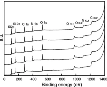
Fig. 2. XPS (X-ray photoelectron spectra) spectra for all the
specimens. study is ‘SiC’; besides the code names of silicon carbide
films with various flow rate of NH gas are ‘SiC–N1’,3 ‘SiC–N2’, ‘SiC–N3’ and ‘SiC–N4’. The flow rate of NH gas for SiC–N1, SiC–N2, SiC–N3 and SiC–N43 were increasing from 250 to 500 sccm. X-Ray photo-electron spectra (XPS) were recorded by a VG Escalab
MKII spectrometer using Al Ka (1253.6 eV) radiation for measuring the composition of silicon carbide films. The infrared spectrometry was performed from 4000 to 400 cmy1 using a Fourier transform infrared (FTIR)
spectrometer calibrated to an unprocessed bare wafer, for determining the chemical structure of the silicon carbide film. The refractive index and thickness of the silicon carbide with or without nitrogen were measured with an n and k analyzer and SORRA ellipsometer. Metal-insulator-semiconductor (MIS) structures of Cuy
silicon carbideysilicon as well as Alysilicon carbidey
silicon were used to investigate the behavior of basic electrical characteristics.
The dielectric constants and leakage current of the SiC films were investigated using capacitance–voltage
(C–V) and current–voltage (I–V) characteristics
meas-urement on MIS capacitor structure. A Keithley Model 82 CV meter at 1 MHz was used to measure the dielectric constant of the film with a gate electrode area of 0.0053 cm . The current–voltage2 (I–V)
characteris-tics of SiC films were measured by an HP4156. The gate-electrode area of the MIS structure was 0.00133 cm for2 I–V measurement.
The completed Al and Cu gated MIS capacitors were then bias-temperature-stressed (BTS) at 150 8C with
gate electrode biases (Vgate). The stress time was 1000
s, which is long enough for the mobile charges to drift
across the stacked insulator layer. The bias was provided by an HP4156Bsemiconductor parameter analyzer.
3. Results and discussions
Fig. 1 shows FTIR spectrum of silicon carbide films with and without the various flow rate of NH3 gas during the deposition process, and the important regions of silicon carbide film were labeled in the figure and indicated as follows. The peak at 780 cmy1is identified as Si–C stretching bond. In addition, Si–CH –Si rock2 and C–H wag peak are near 990 cmy1, C–F bending peak is at 1100 cmy1, Si–CH bending peak is at 1245
3
cmy1, Si–H stretching peak is near 2100 cmy1and C–H stretching peak is near 2960 cmy1. All of these bonds make the surface of the silicon carbide film hydrophobic. From the figure, there were not any nitride derivatives or nitride in any of the samples, and it was obvious that SiC–N1;SiC–N4 have stronger Si–C stretching bonds than the pure silicon carbide, SiC.
XPS spectra for all of the specimens are shown in Fig. 2, and the major peak for Si2p (;100 eV), Si2s
(;155 eV) and C (;285 eV) of every specimens are1s clearly evident in it. The peak of N1s (; 398 eV)
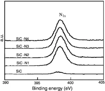
appears in SiC–N1–SiC–N4, but was absent in pure silicon carbide SiC. The enlargements of N1s for all the specimens are shown in Fig. 3. It certificates the exis-tence of SiN bonding in SiCN samples. The peak heights of SiC–N1;SiC–N4 are higher than that of SiC. On the contrary, the carbon contents of the sample SiC–N1;SiC–N4 is smaller than that of SiC. Moreover, the content of silicon remains constant for all the specimens. The atom percentage of nitrogen content for SiC–N1, SiC–N2, SiC–N3 and SiC–N4 is 14.37%,
Fig. 3. Enlargement of XPS spectra of N1Speaks in Fig. 2. The atom percentage of nitrogen content for SiC–N1, SiC–N2, SiC–N3 and SiC–N4 is 14.37%, 15.62%, 16.31% and 16.64%, respectively.
Table 1
The dielectric constant(k) values for all the specimens
SiC SiC–N1 SiC–N2 SiC–N3 SiC–N4
Dielectric 3.83 4.50 4.47 4.34 4.40 constant(k)
Fig. 4. J–E curve on a log (JyE) vs. E1y2 plot of sample SiC–N4 showing Poole–Fenkel conduction at high electric field region. 15.62%, 16.31% and 16.64%, respectively. Although the
change is not significant, the nitrogen content certainly increases with increasing ammonia flow rate during the deposition.
The dielectric constant (k) values for all the
speci-mens were demonstrated in Table 1. The pure silicon carbide film had a dielectric constant approximately 3.8 and the dielectric constants of nitrogen-containing films, SiCN, were higher from 4.3 to 4.5. The increase of dielectric constant is due to the appearance of SiN bonds in a-SiC films. The tetrahedral structure of SiC is distorted with additive of SiN bonds and then polariza-tion chemical structure is raised w9x.
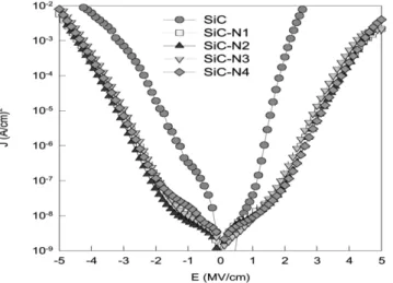
The leakage current densities for all the films are sketched in Fig. 5. It shows clearly that the leakage current of pure silicon carbide(SiC) is much larger than
the doped films. The samples we study are not crystal-lized SiC film but amorphous ones. Nitrogen is not an active dopant without activation process. On the con-trary, a large amount of SiN bonds, which exist randomly in a-SiC films make the structure of a-SiC film more disorderly. In addition, the bonding energy of SiN is higher than SiC bond. The carrier would transport through the SiCN films difficultly. As a result, the leakage currents of a-SiCN films are smaller than a-SiC ones. The curves of SiC–N1–SiCN4 are almost similar so that we can put them on a par. Increasing the temperature increases the leakage current density. Furthermore, the J–E curves are symmetric both in
positive and negatives bias, and the mechanism of leakage current is Poole–Frenkel(P–F) emission as the
electrical field is above 2.5 mVycm. Poole–Frenkel w10x
emission is due to field-enhanced thermal excitation of
trapped electrons in the insulator into the conduction band. The current density is given by:
1y2
BbPFE yfPFE
C F
JsJ exp0
D k TB G
where b s(e y43 p´ ´) ,1y2 f is the contact potential
PF 0 PF
barrier, kB the Boltzmann constant, e the electronic
charge, E the applied electric field, ´0 the dielectric constant of free space, and ´ the relative dielectric constant. Poole–Frenkel mechanism can be identified by comparing the theoretical value of bPF with the experimental value of bexp obtained by calculating the slope of the curve ln (JyE)yE1y2. Fig. 4 shows that the logarithm of leakage current of samples SiC–N4 is linearly related to the square root of the applied electric field, which is closed to Poole–Frenkel emission. The value ofb s5.8=10y23 (Jm yV ) which is close1y2 1y2
exp
to the theoretical value of b s5.72=10y23 (Jm y1y2
PF V1y2) as the dielectric constant is 4.4.
We investigated the impact of thermal annealing on the silicon carbide film. A silicon carbide film, SiC–N4 was annealed at temperature from 400 to 550 8C for more than 1 h in N ambient. Fig. 6 shows the2 J–E
Fig. 5.J–E curves for all the samples. The area of electrodes we used is 0.00133 cm . The leakage current of SiCN based films are lower2
than the a-SiC films. Fig. 7. The relationship of leakage current and stress time for SiCN1 films with Cu and Al gates during BTS test. BTS tests were conducted at 150 8C with electric fields of 4.5 mV and 5.5 mVycm. Dielectric
breakdown is easily occurred at Cu electrode samples at critical BTS condition()4.5 mVycm).
Fig. 6.J–E curves of SiC–N4 samples after thermal annealing at 400, 450, 500 and 550 8C for 1 h. Dielectric properties of SiC–N4 film remain stable up to 550 8C.
Fig. 8. Leakage current–stress time curves of SiC–N4 with CuyAl
gates during BTS at 150 8C. annealing. There is not much change in the leakage
current after thermal annealing. Also, the FTIR spectrum does not vary after thermal treatment. Hence, the thermal treatment at temperature up to 550 8C does not have significant effect on the silicon carbide film. Conse-quently, the thermal stability of silicon carbide film is good enough to meet the prescription in back-end-of-line(BEOL) fabrication process.
The effect of NH flow rate on the barrier ability of3 the prepared samples was also investigated, the flow rate of NH used for the preparation of sample SiC–N43 being twice as high as the one used for preparing SiC–N1. Although the leaky behaviors of both samples are similar, as shown in Fig. 5, we performed the
bias-temperature stress measurement on them(Fig. 6). Bias-temperature stressing (BTS) is a typical manner to estimate the barrier ability against the Cu penetration. We find that SiC–N1 and SiC–N4 exhibit excellent electrical stability even after BTS (3 mVycm, 150 8C, 1000 s). Figs. 7 and 8 exhibit the Igate–tstress curves of SiC–N1 and SiC–N4 with either Al or Cu gate during BTS measurement in high electric field. It is evident that the leakage current of SiC–N1 was almost one order of magnitude larger than that of SiC–N4. It is
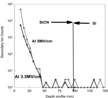
Fig. 9. SIMS depth profile of SiCN4 with Al gate after BTS meas-urement(3.5y5 mVycm, 150 8C, 1000 s). The counts of Al remain
at the same magnitude even after BTS with 5 mVycm for 1000 s at
150 8C.
Fig. 10. SIMS depth profile of SiCN4 with Cu gate after BTS meas-urement (3.5y5 mVycm, 150 8C, 1000 s). The Cu ions obviously
penetrate through the SiCN4 film after BTS with 5 mVycm.
worthy to mention that the leakage current is lower and becomes steady in the electric field below 3.50 mVycm
with increasing stress periods. However, it goes up for electric field greater than 3.75 mVycm as shown in
Figs. 7 and 8. The difference between Cu and Al curves is mainly due to the Cu penetration w11x. When Cu ions were drifted in high electrical field at high temperature, the moving Cu ions would produce the ion current. In addition, the Cu ions are regarded as trap centers in dielectrics, which could assist the carrier to transport
w12x. The leakage currents increase abruptly at 4.5 mVy
cm for SiC–N1 and 5.0 mVycm for SiC–N4 indicating
breakdown.
The difference between the increasing and decreasing behaviors of leakage currents can be explained by material analysis. Figs. 9 and 10 illustrate the secondary ions mass spectra(SIMS) of SiC–N4 with either Cu or
Al electrode after BTS measurement in the condition of 3.5 and 5.0 mVycm for 1000 s at 150 8C. It is clear
that the copper counts in the SiC–N4 layer of the MIS structure after BTS with 5 mVycm are much larger than
that after BTS with 3.5 mVycm, which almost remains
zero. Furthermore, the Al counts remain the same in the silicon carbide layer of the MIS structure after 3.5 mVy
cm BTS and 5.0 mVycm BTS. 4. Conclusions
We have investigated the leaky behavior and barrier characteristics of a-SiCN containing different nitrogen concentrations. The leaky behavior of a-SiCN is Pool– Frenkel in high electric field region. Thermal stabilities of a-SiCN films are good enough to meet the prescrip-tion in BOEL fabricaprescrip-tion process. We performed the bias-temperature stress (BTS) on a-SiCN films to test
the barrier ability against Cu penetration. Experimental results indicate that a-SiCN films containing higher nitrogen concentration exhibited better barrier ability. The dielectric breakdown is due to the penetration of Cu.
References
w1x T. Sakurai, Closed-form expressions for interconnection delay,
coupling and crosstalk in VLSI’s, IEEE Trans. Electron Dev. 40(1993) 118.
w2x A. Mallikarjunan, S.P. Murarka, T.-M. Lu, Metal drift behavior
in low dielectric constant organosiloxane polymer, Appl. Phys. Lett. 79(2001) 1855.
w3x M. Vogt, M. Kachel, K. Drescher, Dielectric barrier for Cu
metallization system, Mater. Adv. Metallization(1997) 51. w4x S.G. Lee, Y.J. Kim, S.P. Lee, H.-S. Oh, S.J. Lee, M. Kim,
I.-G. Kim, J. Kim, H.-J. Shin, J.-I.-G. Hong, H.-D. Lee, H.-K. Kang, Low dielectric constant 3MS a-SiC:H as Cu diffusion barrier layer in Cu dual damascene process, Jpn. J. Appl. Phys. 40(2001) 2663–2668, Part.1, No.4B.
w5x M. Tanaka, S. Saida, T. Lijima, Y. Tsunashima, Low-k SiN
films for Cu interconnects integration fabricated by ultra low temperature thermal CVD, Symposium on VLSI Technology Digest of Technical Papers, 1999, pp. 47–48.
w6x M. Tada, Y. Harada, K. Hijioka, H. Ohtake, T. Takeuchi, S.
Saito, T. Onodera, M. Hiroi, N. Furutake, Y. Hayashi, Cu Dual Damascene Interconnects in Porous Organosilica film with organic Hand-mask and Etch-stop layers For 70 nm-node ULSIs, Proc. IITC2002(2002) 12–14.
w7x M. Foyolle, J. Torres, G. Passemard, F. Fusalba, G. Fanget, D.
O. Louveau, T. Mourier, L. Broussous, Proc. 2002 IEEE IITC
(2002) 39–41.
w8x Z.C. Wu, Y.C. Lu, C.C. Chiang, M.C. Chen, B.T. Chen, G.J.
Wang, Y.T. Chen, J.L. Huang, S.M. Jang, M.S. Liang, Proc. 2002 IEEE IEDM(2002) 595–598.
w9x B.-Y. Tsui, K.-l. Fang, S.-D. Lee, IEEE Trans. Electron Dev.
48(2001) 2375.
w10x S.M. Sze, Physics of Semiconductor Devices, Wiley, New
York, 1981, p. 402, Chapter 7.
w11x A.L.S. Loke, J.T. Wetzel, P.H. Townsend, T. Tanabe, R.N.
Vrtis, M.P. Zussman, D. Kumar, C. Ryu, S.S. Wong, IEEE Trans. Electron Dev. 11(1999) 2178.
w12x P.T. Liu, T.C. Chang, Y.L. Yang, Y.F. Chen, S.M. Sze, IEEE