161R IEEE TRANSACTIONS O N ELECTRON DEVICES, VOL. 41, YO. 9. SEPTEMBER 1994
Effects of Hot Carrier Induced Interface State
Generation in
Submicron LDD MOSFET’s
Tahui Wang, Chimoon Huang,
P.
C. Chou,
SteveS.-S. Chung,
Member, IEEE,and Tse-En Chang
Abstract-A two-dimensional numerical simulation including
a new interface state generation model has been developed to study the performance variation of a LDD MOSFET after a dc voltage stress. The spatial distribution of hot carrier induced interface states is calculated with a breaking silicon-hydrogen bond model. Mobility degradation and reduction of conduction charge due to interface traps are considered. A O.G/tm LDD MOSFET was fabricated. The drain current degradation and the substrate current variation after a stress were characterized to compare the simulation. A reduction of the substrate current at 1; N 0.57;r in a stressed device was observed from both
the measurement and the simulation. Our study reveals that the reduction is attributed to a distance between a maximum channel electric field and generated interface states.
I. INTRODUCTION
S the Si MOSFET technology is moving rapidly into
A
deep submicron domain, hot carrier induced phenomena have spurred great research interest because of their important role in device reliability and characterization [l]-(3].
Recently, it has been recognized that a drain current degradation due to interface state generation is a dominant factor in determination of the device lifetime [ 2 ] , [4]. Extensive studies have been conducted not only on the degradation of device characteristics in the presence of interface states, but also on the physical mechanisms that lie behind the interface state generation [5]-[7]. Among these studies, much effort has been devoted to the experimental characterization of the interface state effects. Numerical analysis of interface state generation and its significance to the device characteristics are rarely reported in the literature.Currently, the lucky electron model and the electron tem- perature model are two commonly used methods to simulate hot electron induced degradation in submicron MOSFET’s. However, the validity of these two model, which are based on assumptions of either a constant mean free path or a Maxwellian type distribution function, is often questioned especially in the simulation of the degradation mechanisms involving extremely high electron energy. Despite the validity of the basic assumptions, a threshold energy of 8.7 eV has to be used for interface state generation in the electron temperature model to fit experimental data [SI. This value is unreasonably large because the electron affinity in Si is only 4.05 eV 191.
On the other side, the lucky electron model also yields a Manuscript received September 21, 1993; revised May IO. 1994. The review of this paper was arranged by Associate Editor A. H. Marshak. This work was supported by the National Science Council. ROC, under Contract Number NSCP, 1 -0404-E-009- 106.
The authors are with the Department of Electronics Engineering, Institute of Electronics, National Chiao-Tung University. Hsin-Chu. Taiwan, R.O.C.
IEEE Log Number 940388 I .
+
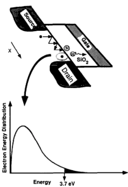
Energy 3.7evFig. I . Illustration of interface state generation. The full circle represents a channel electron. The shaded area under the electron energy distribution represents electrons with energy above the threshold for interface state generation.
doubtful position of interface state generation because the model inherently lacks the nonlocal transport nature. Since the device characteristics are very sensitive to the position of interface states, these two models may lead to an erroneous conclusion or interpretation about the effects of the interface state generation. In this work, we developed a more rigorous window Monte Carlo processor in combination with a breaking Si-H bond model [ l ] to simulate the interface state profile. Our model has been employed in a general-purpose two- dimensional device simulator, Silvaco PISCES-IIB [ lo]. The reduction of channel conduction charge and the degradation of electron mobility due to interface charge are also taken into account in the simulation.
A 0.6pm LDD MOSFET was fabricated to compare the simulation. The drain and the substrate currents before and after a dc voltage stress were characterized. The importance of the position of the interface states to the substrate current characteristics is evaluated through a comparative analysis of the present model and the lucky electron interface state model.
11. DEVICE FABRICATION
A sample n-channel LDD device was fabricated using a polysilicon gate technology. The effective channel length is OOIX-9383/94$04.00 @ 1994 IEEE
WANG et al.: EFFECTS OF HOT CARRIER INDUCED INTERFACE STATE 1619 ri 'E
''
-
0 3 - v-
.-
. a-
500 0 0 4002
01.
-
E !! a-
02 L, iz 3002
P L n -2w.-
U * W 0 3 - 1 0 0 Ej 0 0 4can derive the interface state generation rate as follows: O.Gpm. The gate oxide thickness, spacer width, and channel
width are 140
A,
0.25pm and 20pm, respectively. The &(IC,t )
=CJc,(z)tn
+
N 1 t ( x . 0) (1) threshold voltage adjustment was performed by 70 keV BFzions with a dose of 1012 cniP2. The LDD ri- dose and implant energy are 2.0 x 10''~cm-~ and 80 keV phosphorus. The overlap between the gate and the n- region is about 0.05 pm. The 80 keV arsenic was implanted in the source/drain n+
region at a dose of 3.0 x 1 0 1'm-2 .
The device was stressed at a drain bias of 7 V and a gate bias of 3 V for lo4 s. Under the stress condition, a roughly maximum hot carrier induced degradation rate was obtained.
111. NUMERICAL SIMULATION AND PHYSICAL MODELS
Analysis of the interface state effects caused by hot carrier injection requires a complicated set of physical models in- cluding an interface state generation mechanism, hot carrier injection and nonuniform reduction of conducting electron density and mobility. The physical models employed in the current simulation for the above mechanisms are described in the following.
A . Interface State Generation
The interface state generation is illustrated in Fig. 1 in which channel electrons (represented by full circles) acquire sufficient energy from the large channel field. A fraction of these hot electrons (represented by the shaded area under the energy distribution curve) may have a chance to impinge on the Si/SiO2 interface and to create interface states. Various theories have been proposed to explain the interface state generation mechanism [ 11, [ 5 ] , [ 1
11.
Here. we adopt a breaking Si-H bond model developed by C . Hu et al. [I]. In their model, it is hot electron injection rather than hot hole injection to be responsible for breaking of the Si-H bond. Subsequently, hy- drogen diffusion takes place in the silicon dioxide. Assuming a time-independent hot electron injection current .Jc,, (z), onewhere IC is along the channel direction, Nit(z, 0) is the initial
interface state density, and n is the time-dependence factor of interface state generation. According to the experimental result in [l], n is chosen to be 0.65 in the simulation. C is a fitting parameter to best fit the experimental I-V characteristics. Since Nit(:r, 0) is usually much smaller than the hot electron induced interface state density, it can be neglected in this work.
E . Hot Electron Injection Current
is expressed by
The hot electron current density J , ~ , ( I C ) across the interface
. J c h ( z ) = I d
L
P c ( x ) D ( E ) f ( z , E ) d E (2) where Eit(=
3.7 eV) is the threshold energy for interface state generation.Id
is the drain current.D ( E )
is the electron density of states of a realistic Si pseudopotential band structure.P c ( x )
denotes the probability that electrons impinge on the Si/SiOz interface when they travel in the channel and
f ( x 3 E )
is the electron distribution function. Both and f ( x , E ) are evaluated from a Monte Carlo simulation with a particular hot electron temperature extraction technique. Details of the simulation of .Jch ( : E ) can be found in our previous publication[121.
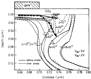
The simulated spatial distribution of the hot electron induced interface states is shown in Fig. 2 (solid line). The stress voltages are V d s = 7 V and V& = 3 V. In the inset of
the figure is the device configuration. The generated interface states have a sharp distribution in space and are positioned in the n- LDD region. The full width at half-maximum (FWHM) of the distribution is about 300
A,
which is consistent with the experimental result obtained from the charge pumping technique [6]. The channel field distribution is also plotted as a reference (dashed line). It should be noted that there exists1620 1 8 - 6 - 4 - 2 - .-O- prestress 0 I 2 3 4 5
Drain Voltage, Vd(volts)
(a) in I 1
I
vg = 5v Simulation Va = 3VI
"
I I -[** 0 ' " " " " ' 0 1 2 3 4 5Drain
Voltage, Vd(volts)
(b) Fig. 4.
and (b) simulated I,( versus I;, characteristics before and after a stress. (a) Measured 1,l versus 1
:,
characteristics before and after a stress,a distance of about 400
A
between the maximum electric field and the peak of the interface state distribution. This distance is required to transform the acquired kinetic energy into thermal energy via phonon scattering. The equipotential contours before and after a stress in Fig. 3 show the interface trap effect on the potential distribution in the device. The position of interface states is indicated by crosses in the figure. It is found that the electric field distribution in the high field region tends to spread more widely after a stress.C. Mobility Degradation and Conduction Charge Reduction Because of the presence of acceptor-type interface states, channel electrons may be trapped at the interface to form negative interface charge. As a result, the threshold voltage has a positive shift and the quantity of conduction charge reduces.
IEEE TRANSACTIONS ON ELECTRON DEVICES, VOL. 41, NO. 9, SEPTEMBER 1994
Si02
I
0 00 0.02 0.04 0.06 0.08 0.10 0 1 2 Distance ( p m )Fig. 5 . Simulated two-dimensional distributions of electron concentration before and after a stress. The unit for electron concentration is C I I I - ~ . Current
flows are shown by the thick solid line (before stress) and the thick dashed line (after stress). The position of interface charge is marked by crosses.
The amount of charge trapped at the interface depends on the position of the quasi-Fermi level with respect to the band edge. In addition, an empirical mobility degradation formula [ 131
arising from Coulomb scattering due to interface charge is incorporated in the two-dimensional device simulation. Now, once interface charge is calculated, its influence on the reduc- tion of conduction charge and the mobility degradation can be immediately evaluated.
Iv.
RESULT AND DISCUSSIONThe experimental and simulated drain currents before and after the hot electron stress are shown in Fig. 4(a) and Fig. 4(b). Good agreement between experiment and simulation has been achieved with a maximum interface state density
of 1.2 x 10¹²/cm2 in the simulation. The drain current degradation in the saturation region is much smaller than in the linear region. The reason is that a channel depletion exists in the n- region, where the generated interface states are located, due to a large drain voltage in the saturation region. The low electron quasi Fermi level in the depletion region results in minimal electron occupation of interface states. Thus the effects of mobility degradation and conduction charge reduction are smaller in the saturation region and so is the drain current degradation. It should be pointed out that no oxide charge incurred threshold voltage shift is observed from the drain current characteristics. In the linear region, the amount of trapped interface charge becomes significant. An appreciable drain current degradation appears. The degradation can be well explained by Fig. 5 where the two-dimensional distributions of electron concentration with
a
current flow before and after a stress are plotted. Apparently, interface charge (marked by crosses in the figure) results in a decreaseof electron concentration underneath and accordingly the current flows deeper in the interface state region. A drop in the slope of the stressed I d - Vd characteristics actually reflects the interface state effects.
WANG el al.: EFFECTS OF HOT CARRIER INDUCED INTERFACE STATE
1
1621
I"
0 2 4 6 8 10
Gate Voltage, V, (volts)
(a) = 6V
-
prc-slress.--
post-stressI "
1
---
10Gate Voltage, V, (volts)
(b) Fig. 6.
simulated substrate current before and after a stress,
(a) Measured substrate current before and after a stress, and (b)
The measured and simulated substrate currents at a drain bias of 6 V are presented in Fig. 6(a) and Fig. 6(b). Except for a small deviation at a large gate bias caused by an overestimate of the impact ionization rate in a Monte Carlo model, the simulated substrate current is quite consistent with the experimental result. Both the simulation and the measurement show a reduction of the substrate current at a low gate bias (for example,
5;
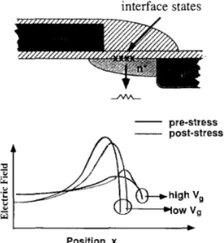
= 3 V) and an enhancement at a high gate bias (for example, 1.; = G V) after the stress. In order to explain the variation of the substrate current, the electric field distributions at a low gate bias and at a high gate bias are depicted in Fig. 7. At a low gate bias, the interface states are about a few hundredA
behind the maximum electric field as mentioned previously. Since the interface state generation can be treated as an increase of the channel resistance, a larger voltage drop develops in the interface state region to compensate for the increased channel resistance. Consequently, the maximum electric field, which is outside the interface state region, declines after the stress andso does the substrate current. As the gate bias increases, the maximum channel field shifts toward the interface state region.
interface states
-
pre-stress-
post-stress U U-
5 U L 3 U.-
z
Position, x Fig. 7.due to interface states.
Schematic representation of the variation of the channel electric field
h
3
v c) L 3 U 0) YE
* n a LA 80-
60-
40 - 20 --
pre-stress posi-strcss(our model)post-swss(lucky electron model)
Fig. 8. The calculated substrate currents from our model and from the lucky electron model. The solid line represents the substrate current before a stress.
While the maximum field and the interface states occupy almost the same region, a larger voltage drop in the interface state region implies an increase of the maximum field. Thus the substrate current shows an enhancement instead at a larger gate bias.
In order to further evaluate the significance of the interface state position to the substrate current, we make a comparison between the present model and the lucky electron interface state model. The reader should be reminded that the interface state generation rate in the lucky electron model is a function of only a channel electric field. The peak of the interface state density occurs at the same position as the maximum electric field. For the purpose of a comparison, the same density of interface states is used in both models. The calculated substrate currents versus gate bias are shown in Fig. 8. As expected, the lucky electron model predicts a higher maximum electric field and an enhancement of the substrate current. This result is obviously opposite to the measured characteristics due to the small deviation
in
the location of the interface states.1622 IEEE TRANSACTIONS ON ELECTRON DEVICES. VOL. 41, NO. 9, SEPTEMBER 1994
V. CONCLUSION Chimoon Huang was bom in Chdng-Hua, Taiwan, on October 15, 1964. He received the B S degree in electrical engineering from National Taiwan Ocean University 111 1986. Currently, he is working towards the Ph.D. degree in electrical engineenng at Na- tional Chiao-Tung University, His current research interest is in the characterization and simulation of A combined Monte Carlo method and the breaking Si-H
bond model has been developed to simulate the effects of in- terface state generation. Good agreement between experiment and simulation is achieved. The implications of a distance
between the maximum electric field and the hot electron hot camer effects in wbmicron MOSFET’s induced interface states have been discussed.
REFERENCES
C. Hu, S. C. Tam, F. Hsu, P. Kuo, T. Chdn, and K. W. Terrill, “Hot-electron-induced MOSFET degradation-model, monitor, and im- provement,” IEEE Trans. Electron Devices. vol. ED-32, pp. 375-385.
Feb. 1985.
Y. Toyoshima. H. Iwai, F. Matsuoka, H. Hayashida, K. Maeguchi, and K. Kanzaki, “Analysis on gate-oxide thickness dependence of hot-camer-induced degradation in thin-gate oxide nMOSFET’s,” IEEE Trans. Electron Devices, vol. 37, pp. 1496-1503, June 1990.
W. Hansch, C. Mazure, A. Lill, and M. K. Olowski, “Hot carrier hard- ness analysis of submicrometer LDD devices,” IEEE Trans. Electron Devices, vol. 38, pp. 512-517, Mar. 1991.
P. Heremans, R . Bellens, G. Groeseneken, and H. E. Maes. “Consis- tent model for the hot-camer degradation in n-channel and p-channel MOSFET’s,” IEEE Trans. Electron Devices. vol. 35, pp. 2194-2209,
Dec. 1988.
H. Gesch, J. P. Leburton, and G. E. Dorda, “Generation of interface states by hot hole injection in MOSFET’s,” IEEE Trans. Electron Devices. vol. ED-29, pp. 913-918, May 1982.
M. G . Ancona, N. S. Saks, and D. McCarthy, “Lateral distribution of hot-carrier-induced interface traps in MOSFET’s,” IEEE Truns. Electron
Delices, vol. 35, pp. 2221-2228, Dec. 1988.
J-J. Shaw and K. Wu, “Determination of spatial distribution of interface states on submicron lightly doped drain transistors by charge pumping measurement,” IEDM Tech. Dig., pp. 83-86, 1989.
F. Ootsuka. “The evaluation of the activation energy of interface state generation by hot electron injection,” IEEE Trans. Electron Devicer.
vol. 38, pp. 1477-1483, June 1991.
S. M. Sze, Physics of Semiconductor Devices. 2nd ed. New York: Wiley, 1981.
M. R. Pinto, C. S. Rafferty, H. R. Yeager, and R. W. Dutton, “PISCES- IIB Poisson and continuity equation solver,” Stanford Electrons Lab., Stanford Univ., Palo Alto, CA, 1986.
E. Takeda. A. Shimizu, and T. Hagiwara, “Role of hot hole injection in hot carrier effects and the small degraded channel region in MOSFET’s,”
IEEE Electron Dev. Lett., vol. EDL-4, pp. 329-331, Sept. 1983. C. Huang, T. Wang, C. N. Chen, M. C. Chang. and J. Fu, “Modeling hot-electron gate current in Si MOSFET’s using a coupled drift-diffusion and Monte Carlo method,” IEEE Trans. Electron Devices, vol. 39, pp.
2562-2568, Nov. 1992.
S. C. Sun and J. D. Plummer, “Electron mobility and accumulation layers on thermally oxidized silicon surfaces.” IEEE Truns. Electron D e ~ i ~ e s , vol. ED-27, pp. 1497-1508, Aug. 1980.
Tahui Wang was born in Taoyuan, Taiwan, on May 3, 1958. He received the B.S. and the Ph.D. de- grees in electrical engineering from National Taiwan University and the University of Illinois, Urbana- Champaign in 1980 and 1985, respectively.
From 1985 to 1987, he joined the High-speed De- vices Laboratory of Hewlett-Packard Labs, where he was engaged in the development of compound semiconductor devices and circuits. Since 1987, he has been with the Department of Electronics En- eineerine and the Institute of Electronics. National Chiao-Tung University. ;here hye is now a Full Professor. His’ research interests include hot carrier phenomena characterization and reliability physics in Si MOSFET’s, and modeling and simulation of GaAs quantum well devices and circuits.
In 1991, he was granted a Best Teaching Award by the Ministry of Education.
P. C. Chou, photograph and biography not available at time of publication.
Steve Shao-Shim Chung (S’83-M’85) received the B.S degree from the National Cheng-Kung University, Taiwan, in 1973, the M.Sc degree from the National Taiwan University, in 1975 and the Ph.D degree from the University of Illinois at Urbana-Champaign, in 1985, all in electrical engi- neering.
From 1976 to 1978, he worked for an electronic instrument company as Head of the R&D division and subsequently as Manager of the Engineering Division. From 1978 to 1983, he was with the department of Electronic Engineering and Technology at the National Taiwan Institute of Technology (NTIT) as a Lecturer. He was also in charge of an Instrument Calibration Center at NTIT. From 1983 to 1985, he held a research assistantship in the Solid State Electronics Laboratory and the Department of Electrical and Computer Engineering at the University of Illinois In September 1985, he served at NTIT again as an Associate Professor in the Department of Electronic Engineering. Since August 1987, he has been with the Department of Electronic Englneerlng and Institute of Electronics. NdtiOnd Chiao Tung University, and has been a Full Professor since the Fall of 1989 His current teaching and research Interests are in the areas of solid- state device physics and VLSI technology, semiconductor device modeling and simulation, characterization and reliabtlity study of VLSI devices and circuits. and computational algorlthms for VLSI circuits.
Dr. Chung has served as a Technical Program Committee Member of the ASIC Conference, IEEE, since 1989.
Tse-En Chang was bom in Yun-Lin, Taiwan, on October 17. 1969. He received the B.S. degree in electronic engineering from National Chiao-Tung University in 1992. Currently, he is working towards the Ph.D. degree in electronic engineering at Na- tional Chiao-Tung University. His current interest is in the modeling and simulation of submicrometer semiconductor devices.