From eqn. 3, it is clear that the log-gains of all channels are lin- ear functions of the reservoir r only. We can also rewrite eqn. 3 in a more familiar form as Gk(t) = pLri,(o?x(t) - (T:), where x ( t )
4
(l/L)J,LN,(z, t)dz is the mean fraction of excited ions [2].Multiplying both sides of eqn. 1 by dz and integrating from 0 to L yields
Using eqn. 3 in eqn. 4, we finally obtain a first-order differential equation describing the dynamic time behaviour of the system’s state, i.e. the reservoir r(t):
Once the initial condition r(0) = r, is specified, the solution of eqn. 5 is unique. ro can be any number in the allowed range [0, PAL]. However, if at time t = @, i.e. one instant before the start of the observation period, the amplifier is at equilibrium, then r, must satisfy eqn. 5 with i(@) = 0:
N
3=0
which is the well-known Saleh steady state equation [3]. For a starting guess in its numerical solution, the upper bound
zC,”io Q:(O-) can be used.
Note that, since by eqn. 5 the derivative of r exists, r is a contin- uous function of t , even when the inputs {
Qp}
are discontinuous. In exactly the same way as for charge on a capacitor, the reservoir cannot ‘jump’ instantaneously. Note also that eqn. 5 has a nice physical meaning: the variation of the reservoir (the ‘charge’ on the amplifier) is given by the total input flux C:OQ”’, minus the output flux CJoQy‘,
minus the spontaneous decay from the excited level Y/T.Hence, by identifying photon fluxes with currents, and the res- ervoir with the charge on a capacitor, or better yet with the volt- age across a capacitor of capacity C = 1, we obtain the equivalent electric circuit depicted in Fig. la. The circuit is composed of N input current sources (the channels) and of a pump channel 0, hid- den inside the amplifier. The currents feed the capacitor, whose voltage is the reservoir r . The currents out are voltage-controlled current generators, whose gain is g,(r) = eGi@). The output pump current is shunted to ground and does not exit the amplifier. The RC constant of the capacitive circuit is
z.
However, this is an active circuit, and it is clear that the actual time constants involved in the dynamics are essentially independent of 7 .pump removed
b
m Fig. 1 Fibre amplifier equivalent circuit and that f o r optical loss L a Fibre amplifier equivalent circuit
b For optical loss L
1888
The circuit model for a subsequent loss L is shown in Fig. lb. It is simply a bank of current-controlled current generators that shunt part of the output photons to ground, effectively wasting them.
Using these building blocks for the amplifier and the loss, any complex network of amplifiers is readily solved by any electric cir- cuit simulator available on the market.
Acknowledgments: This work was supported by the European Community under NCO-DC project No 950959 ‘DAWRON, and by an NSERC Industrial Chair sponsored by QuCbec-TtlC- phone.
0 IEE 1997
Electronics Letters Online No: 19971273
A. Bononi (Universita di Parma, Dipartimento di Ingegneria dell’lnformazione, 1-43100 Parma, Italy)
&.A. Rusch and L. Tancevski (Universitd Laval, Dipartement de Gdnie
Electrique et de GPnie Informatique, Quebec, G l K 7P4, Canada) 21 July 1997
References
SUN, Y., LUO, G., ZYSKIND, J.L., SALEH, A.A.M., SRIVASTAVA, A.K , and SULHOFF, J.w.: ‘Model for gain dynamics in erbium-doped fibre amplifiers’, Electron. Lett., 1996, 32, pp. 1490-1491
GEORGES, T , and DELEVAQUE, E.: ‘Analytic modeling of high-gain erbium-doped fibre amplifiers’, Opt. Lett., 1992, 17, pp. 11 13-1 115 SALEH, A.A.M., JOPSON, R.M., EVANICOV, J.D., and ASPELL, J.: ‘Modeling of gain in erbium-doped fibre amplifiers’, IEEE Photonics Technol.
Lett., 1990, 2, pp. 714717
Suppression of optical beat interference using
synchronised GDNIA technique and
in-band clipping carrier
B.H.
Wang,C.C.
Hsiao andW.I.
WayIndexing terms: Code division multiple access, Multi-access systems, Optical communication
The authors propose adding a coherent in-band clipping carrier to a previously demonstrated Walsh-code-based synchronised CDMA (S-CDMA) technique to firther suppress the optical beat interference (OBI). Experimental results showed that a negligible system power penalty can be achieved even when the OBI-induced intensity noise was as high as -90.9dBMz. In addition, a large system dynamic range of lOdB can be obtained to relax the tight power control requirement on S-CDMA signals.
Introduction: The feasibility of using a Walsh-code-based synchro- nised CDMA (S-CDMA) technique to achieve multiple access in the presence of optical-beat and co-channel interference was previ- ously demonstrated [l]. While conventional OBI suppression tech- niques such as out-of-band clipping-tone [2, 31 or over-modulating multiple frequency-division-multiplexed channels [4, 51 could cause in-band nonlinear distortions, the S-CDMA technique can effec- tively suppress the OBI without incurring the same problem and at the same time enjoy the full bandwidth of an optical fibre system.
However, owing to the fact that a broadband CDMA cannot sup-
press OBI as effectively as narrow-band clipping tones, we found that some residual system penalties remained due to incomplete suppression of the OBI [l]. Therefore, in this Letter, we propose adding an in-band clipping carrier to the S-CDMA signal, to fur- ther suppress the residual OBI without using additional system bandwidth. By implementing this technique, the power control tol- erance of the optical transmitters can be relieved by -8dB com- pared to that of the previous case 111.
Experiment: Our experimental setup is shown in Fig. 1. An S- CDMA signal and an in-band clipping carrier were coherently combined and used to modulate a 1 . 3 ~ DFB laser (laser A). The S-CDMA signal was generated by spreading a 1.5625Mbit/s, 2*O-l ELECTRONICS LETTERS 23rd October 1997 Vol. 33 No. 22
pseudorandom data with a 200Mbitis Walsh code (using Walsh code generator#l) which had a code length of 128, and was up- converted by a 672MHz R F carrier. Note that the 672MHz car- rier served as both the upconverter local oscillator and the in-band clipping carrier. The OBI was generated by using laser B and a delayed self-homodyne interferometer (DSI) setup. Various OBI levels were obtained by adjusting the tunable optical attenuator following the DSI. The modulation indices in both laser A and B were adjusted to be the same. The received signal and the OBI were both down-converted by a perfectly-phase-locked 672MHz carrier and subsequently de-spread by a perfectly-synchronised Walsh code. -32 E -30 a“ -28 -26 Transmitted Data
-
a-
+
m-
-
Fig. 1 Experimental setup
The minimum received optical power from laser A, PA, at a photo-detector when the BER = l V 9 was measured for four differ- ent cases: (i) S-CDMA signal modulation without OBI; (ii) S- CDMA signal and in-band clipping carrier modulation without OBI; (iii) S-CDMA signal modulation with OBI and (iv) S- CDMA signal and in-band clipping carrier modulation with OBI. In the measurement we arbitrarily let the S-CDMA signal and clipping carrier have equal power, i.e. MIs = MIc (MZs and MIc are the modulation indices of the S-CDMA signal and clipping carrier, respectively). Fig. 2 shows the measured results when the
received optical power from DSI, P,, is -19dBm. We can see that, with OBI present, the minimum PA can be improved by -5dB due to the addition of a clipping carrier. However, when comparing cases (i) and (ii), we note that there is a < 2dB system power penalty. This is because the clipping carrier introduced some non- linear distortions into the S-CDMA signal.
-34
,
1 0t
at
A 0a
A a t A A A -24 I I I I I 130 140 150 160 170 180 MI =MI c , % /589121Fig. 2 Minimum required received power from laser A ( P A ) at BER =
against CDMA signul modulation index MIs and clipping carrier modulation index MIc
0 S-CDMA only, no OBI
+
S-CDMA and clipping carrier, no OBIS-CDMA and clipping carrier, with OBI
A S-CDMA only, with OBI
Fig. 3 illustrates the RF spectra of OBI before and after’the S- CDMA signal and a coherent in-band clipping carrier were applied. The modulation indices of both signals were 180% and P,
= -19dBm. It can be seen that the OBI level was suppressed by at least lOdB and the peak OBI level was suppressed by as much as 37dB.
ELECTRONICS LETTERS 23rd October 1997 Vol. 33 No.
...
I
centre 672 MHz span 1 GHz
889131
Fig. 3 Spectra of OBIS before and after S-CDMA and in-band clipping carrier were applied
Modulation indices of both applied signals were 180%
a Before b After I U
*
*
A A e a m W 10.’ i o - * 10.’ 9 I I a = I . . . T , B4
f -34 -32 -30 -28 -26 P A, dBmFig. 4 BER against Pa f o r three different levels of OBI M I , = M I , = 180%
0 RIN,,, = -90.9dB/Hz, P, = -19dBm
+
RIN,, = -81.5dB/Hz, PE = -16dBmRINoBI = -ll.ldB/Hz, P, = -13dBm
A No OBI
clipping carrier modulation index MI c,%
180 162 140 120 80
-27
I
I
I I I I I
80 100 120 140 160 180
signal modulation index MI , %
1689151
Fig. 5 Minimum required received power from laser A f o r different combinations of clipping carvier and C D M A signal when total driving power was fixed
Fig. 4 shows the measured results when MIs = MIc = 180%, for the cases of no OBI and OBI levels given by RIN,, = -90.9, -81.5 and -77.7dB/Hz, respectively. Here, RIN,,, is defined as < i & H IAz where i& is the spectral density of the OBI noise current and I, is the received photocurrent from laser A. It is interesting to
note that there was a negligible system power penalty even when the OBI level was as high as -90.9dBlHz. In addition, if we con- sider the system dynamic range (DR) as the ratio of maximum to minimum allowable received optical power [4], it is given by (P, -
3) - PA [dB] and is -1OdB for RZN,, = -81.5 or -77.7dBMz. This
is much higher than the 2.5dB DR obtained previously when the
clipping carrier was absent [1]. Consequently, the power control requirement on S-CDMA technique can be relaxed significantly.
Although the added coherent clipping carrier provides an excel- lent OBI suppression capability and a large system DR, it con- sumes a significant amount of R F driving power to laser A. Conversely, it is conjectured that the clipping carrier can suppress OBI more effectively than the S-CDMA signal. It is therefore important to find a balance between the driving power levels of the clipping carrier and the S-CDMA signal. Fig. 5 shows the results of PA against different values of MIs and MI, when the total driving power was fixed. We can see that there indeed exists an optimum (coherent) combination of the clipping carrier and the S-CDMA signal power, i.e. a minimum PA of -30.5dBm was obtained when MI, = 150% and MI, = 130%. Also, when most of the driving power is allocated to either the clipping carrier or the S-CDMA signal, the resultant power levels of PA were increased by 3dB compared to the optimum case.
Conclusion: In this Letter, we have experimentally demonstrated that an in-band clipping carrier, when coherently combined with a Walsh-code-based S-CDMA signal, can effectively suppress OBI in a PON or WDMA network. When the total driving power was fixed, we found that an optimum combination ratio of the two sig- nals exists to achieve a maximum system power budget. Our experimental results showed that, under the condition of no band- width wasted on the in-band clipping carrier, a negligible system power penalty can be achieved even when the OBI-induced inten- sity noise was as high as -90.9dB/Hz. In addition, a large system dynamic range of lOdB can be obtained to relax the tight power control requirement on S-CDMA signals.
0 IEE 1997
Electronics Letters Online No: 19971275
23 July 1997
B.H. Wang, C.C. Hsiao and W.I. Way (Department of Communication
Engineering, National Chiao-Tung University, Hsin-Chu, Taiwan, Republic of China)
E-mail: [email protected] References
HSIAO, c.c., WANG, B.H., and WAY, w.I.: ‘Multiple access in the presence of optical-beat and co-channel interference using Walsh- code-based synchronised CDMA technique’, IEEE Photonics
Technol. Lett., 1997, 8, pp. 1173-1175
WOODWARD, s.L., LU, x., DARCIE, T.E., and BODEEP, G.E.: ‘Reduction of optical-beat interference in subcarrier networks’, IEEE
Photonics Technol. Lett., 1996, 8, pp. 694696
SASAI, H., YAMAMOTO, H., UTSUMI, K., and FUJITO, K.: ‘Optical access links suppressing optical beat interference with FP-LDs for microwave transmission’. Int. Topical Meeting on Microwave Photonics, Tech. Dig., 1996, pp. 237-240
optical beat interference on the dynamic range of a subcarrier multiple access passive optical network using Fabry-Perot laser’, J. Lightwave Technol., 1996, 5, pp. 711-715
WOOD, T.H., and SHANKARANARAYANAN, N.K.: ‘Operation of a passive optical network with subcarrier multiplexing in the presence of optical beat interference’, J. Lightwave Technol., 1993,
FELDMAN, R.D., WOOD, T.H., RAYBON, G., and AUSTIN, R.F.: ‘Effect Of
10, pp. 1632-1640
Optical signal processing based on time-space-conversion is highly attractive, especially for ultrafast signal processing applications in high-speed optical communcation systems with a data rate of more than 100 Gbit/s. Such processing enables many operations such as the formation, reshaping, pattern recognition and even routing of an ultrafast bit stream, which are difficult to do by tra- ditional electronic means. This technology has been widely demon- strated in the wavelength range of 0.4-0.85p by using free-space optics with diffraction grating pairs and lenses [l - 41. In such a
grating system, however, the time window is determined by the size of the diffraction grating and spatial filter, and it is difficult to make it compact.
In this Letter, we propose time-space-conversion optical signal processing using an arrayed-waveguide grating (AWG) and dem- onstrate pulse train generation at the communication wavelength of 1 . 5 5 ~ .
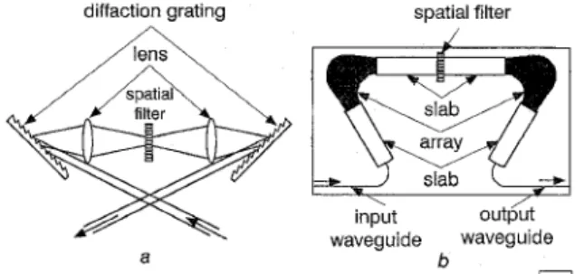
diffaction grating spatial filter
a b
Fig. 1 Schematic diagram of time-space-conversion processing system
using diffraction gratings (DGs), and arrayed-waveguide gratings ( A WGs)
a DGs
b AWGs
Fig. 1 shows a schematic diagram of time-space-conversion processing systems using a diffraction gratings (DGs) and b arrayed-wavegwde gratings (AWGs). In both systems, a temporal waveform carries spatial information on the dispersive element and is converted to a temporal frequency spectrum in the focal plane. The frequency spectrum is then modulated in parallel by a spatial fiiter and reconverted to a reshaped temporal waveform. When the waveform u(t) is incident on the dispersive elements, such as a DG and an AWG, with the incident angle so as to pro- duce the surface normal diffracted beam with the carrier lightwave frequency vo, it is transformed into u(t - nipxic) on the x axis lying
along the exit surface of the dispersive element, where
p
is a dis- persion parameter, c is the speed of light, and n is the refractive index of the media through which the light propagates. The dis- persion parameter is given aswhere m is the diffraction order and d is the periodical pitch of the dispersive elements. The maximum time window To is determined by npxic, hence:
where N is the number of illuminated lines of the D G or waveguides of the AWG. The diffraction order of the D G is lim- ited to a small value, typically m = 1, as it is proportional to the grating pitch, whereas AWGs usually have a large diffraction order (30-200) as it is proportional to the path length difference between neighbouring waveguides [5]. This means we have some
design flexibility in that the dispersion parameter value can be
made quite large for an arbitraray diffraction order in the AWG
Time-space-conversion optical signal processing
using arrayed-waveguide grating
system: and this results in a long total time window even if N is limited to a smaller value than that in the DG system.
Conversely, in the DG system pulsewidth
z
in the pulse trains is T. Kurokawa, H. Tsuda,K.
Okamoto, K. Naganuma,H. Takenouchi, Y. Inoue and M. Ishii
usually limited by the spatial filter size, H, as follows:
Indexing terms: Optical communication equipment, Gratings in fibres
integration capabilities. Pulse train generation is demonstrated to confirm its performance at the wavelength of 1.55 pun.
1IL
r > -
U0 (4)