860 IEEE PHOTONICS TECHNOLOGY LETTERS, VOL. 22, NO. 12, JUNE 15, 2010
Study of InGaN–GaN Light-Emitting Diodes With
Different Last Barrier Thicknesses
Jun-Rong Chen, Tien-Chang Lu, Member, IEEE, Hao-Chung Kuo, Senior Member, IEEE,
K. L. Fang, Member, IEEE, K. F. Huang, C. W. Kuo, C. J. Chang, C. T. Kuo, and
Shing-Chung Wang, Life Member, IEEE
Abstract—This work reports a theoretical and experimental
study on the device performance of blue InGaN–GaN light-emit-ting diodes (LEDs) with different last barrier thicknesses. The experimental results show that the employment of a 25-nm-thick p-type GaN last barrier in GaN LEDs can improve the light output power from 35.6 to 40.2 mW at 50 mA. By using advanced device simulation, it is shown that the effective energy barrier created by the p-type AlGaN electron blocking layer (EBL) is significantly decreased due to the band bending at the interface between GaN last barrier and AlGaN EBL. The use of a p-type GaN last barrier before the growth of AlGaN EBL can provide a higher energy barrier to suppress the electron overflow and then enhance the light output power.
Index Terms—Electroluminescence, electron overflow, light-emitting diodes (LEDs), quantum wells (QWs).
I. INTRODUCTION
H
IGH-BRIGHTNESS nitride-based blue and green light-emitting diodes (LEDs) have been developed in various applications due to the widely tunable wavelength from ultra-violet to green [1]. Recently, the light extraction efficiency of GaN LEDs has been significantly improved by the use of pat-terned sapphire substrates [2], surface roughness [3], nanostruc-ture on the LED surface [4], and photonic crystals [5]. Neverthe-less, the internal quantum efficiency (IQE) still suffers several issues, including the high dislocation density, the quantum-con-fined-Stark effect (QCSE), the low hole concentration in p-type GaN, and the severe electron overflow. These problems result in the slow improvement in IQE of GaN-based LEDs. Recently, the engineering of GaN LED structures has played an important role in the improvement of IQE and has attracted many research groups devoted to this field. By properly designing the active re-gion structures, the built-in polarization field can be effectivelyManuscript received November 28, 2009; revised January 23, 2010; accepted March 14, 2010. Date of publication April 05, 2010; date of current version May 21, 2010. This work was supported in part by the National Science Council in Taiwan under Grant NSC96-2221-E-009-095-MY3 and Grant NSC96-2628-E-009-017-MY3.
J.-R. Chen, T.-C. Lu, H.-C. Kuo, and S.-C. Wang are with the Department of Photonics and Institute of Electro-Optical Engineering, National Chiao Tung University, Hsinchu 30050, Taiwan (e-mail: jrchen.eo95g@nctu.edu.tw; timtclu@faculty.nctu.edu.tw; hckuo@faculty.nctu.edu.tw; scwang@cc.nctu. edu.tw).
K. L. Fang, K. F. Huang, C. W. Kuo, C. J. Chang, and C. T. Kuo are with the Tech. and Product R&D Department, Lextar Electronics Corporation, Hsinchu 30075, Taiwan (e-mail: Hardy.Fang@lextar.com; KF.Huang@lextar.com; CW.Kuo@lextar.com; CJ.Chang@lextar.com; CT.Kuo@lextar.com).
Color versions of one or more of the figures in this letter are available online at http://ieeexplore.ieee.org.
Digital Object Identifier 10.1109/LPT.2010.2046483
controlled, resulting in the suppression of electron overflow [6], [7]. Although a p-type AlGaN electron blocking layer (EBL) is commonly employed in GaN-based LEDs to create an energy barrier, the issue of electron overflow is still severe especially at high injection current densities. In this study, we used a rela-tively thicker p-type GaN last barrier to improve the light output power before the growth of AlGaN EBL. The simulation results show that the electron overflow can be effectively inhibited after employing a thick p-type GaN last quantum barrier in the GaN LEDs.
II. EXPERIMENTS
The epitaxial InGaN–GaN LED structures were grown on -plane sapphire substrates by metal–organic chemical vapor deposition (MOCVD). After thermal cleaning of the substrate in hydrogen ambient for 5 min at 1100 C, a 30-nm-thick GaN nucleation layer was grown at 500 C. On the top of the low-temperature GaN layer, a 2- m undoped GaN was grown at 1100 C, followed by a 2- m Si-doped n-type GaN layer grown at 1050 C ( cm ). After the growth of the buffer layer, six-period InGaN–GaN multiple quantum wells (MQWs) were grown, followed by a p-type Al Ga N EBL and a 120-nm p-type GaN contact layer. The Mg doping con-centrations in the p-type GaN last barrier, AlGaN EBL, and p-type GaN contact layer are about , , and cm , respectively, from the measurement of the sec-ondary ion mass spectrometry (SIMS) and the Al composition in AlGaN is estimated by performing HRXRD measurement. The MQW active region consists of 3-nm-thick InGaN wells and 8-nm-thick GaN barriers. Subsequently, the LED mesa with an area of 250 580 m was defined by using standard pho-tolithography and dry etching. In addition, a transparent con-duction indium–tin–oxide (ITO) layer was employed to be the p-type Ohmic contact layer and Cr–Pt–Au metal was deposited as p- and n-type electrodes, respectively. Three LED samples were prepared in this study. The reference LED with 8-nm un-doped last barrier layer is labeled by Sample A. Samples B and C are the LEDs with insertion of 25- and 75-nm p-type GaN last barriers, respectively. The undoped 8-nm GaN last barrier was still kept in Samples B and C to avoid the Mg diffusion into the MQWs [8]. The LED devices were measured under con-tinuous-wave condition at room temperature (RT) and the light output was collected by integration sphere. The measured op-tical power was calibrated from TO-can database.
CHEN et al.: STUDY OF InGaN–GaN LEDs WITH DIFFERENT LAST BARRIER THICKNESSES 861
Fig. 1. (a) ExperimentalL–I–V characteristics of Samples A, B, and C mea-sured at RT. (b) Simulation results of theL–I–V characteristics of Samples A, B, and C.
III. RESULTS ANDDISCUSSION
Fig. 1(a) shows the measured light–current–voltage ( – – ) characteristics of the GaN LEDs with different last barrier thick-nesses at RT. The output powers of Samples B and C show ob-vious improvement as compared with that of Sample A. The output power increases from 35.6 to 40.2 mW at 50 mA after inserting the 25-nm-thick p-type GaN last barrier. The increase of p-type last barrier thickness from 25 to 75 nm cannot fur-ther enhance the output power but gives rise to an additional series resistance due to the low hole mobility in highly doped p-type GaN [9] and the high activation energy of Mg dopants [10], which leads to slight increase in forward voltage. In order to further investigate the physical mechanisms responsible for the improvement of light output powers in Samples B and C, nu-merical simulations of these LED structures with different last barrier thicknesses are performed using the APSYS simulation software. The simulated structures, such as layer thicknesses, doping concentrations, and Al composition are the same as the actual devices and the corresponding nitride material parameters are used in the calculations [11], [12]. We use an Mg activation energy of 170 meV for GaN which is assumed to increase by 3 meV per % Al for AlGaN [13], [14]. The Shockley–Read–Hall (SRH) recombination is directly governed by the defect-related nonradiative SRH lifetime ( ). In this study, we employ a common value of ns in our simulation [15], [16]. The detailed physical models about the simulation can be found in [15]. Fig. 1(b) plots the calculated – – characteristics of these three LED samples. The calculated output power is deter-mined by using a light extraction value of 82% in the three LED structures to match the order of the experimental output power since we use the same process technique to rough the LED sur-face. From the simulation results, similar trends (i.e., the im-proved output power and slightly increased forward voltage) are observed after employing the p-type GaN last barrier. Fig. 2 shows the simulated energy band diagrams of these three LED samples when the input current is 50 mA. In Fig. 2(a), the en-ergy barrier height created by AlGaN EBL is substantially re-duced by the strong band bending, which is inre-duced by the high density of positive polarization charges at the interface between the GaN barrier and the AlGaN EBL. This band bending will cause electrons accumulating at this interface and then leads to severe electron overflow [17]. On the contrary, when we inset a p-type GaN last barrier layer before the growth of AlGaN EBL, the interface of band bending is pushed away from the MQW
Fig. 2. Calculated energy band diagrams under an injection current of 50 mA for the LEDs with different p-type GaN last barriers.
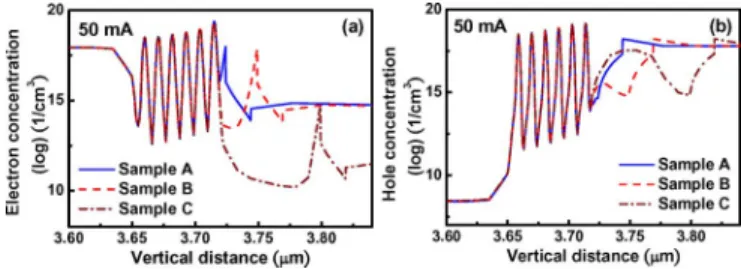
Fig. 3. Calculated electron and hole concentration distributions for Samples A, B, and C under the injection current of 50 mA at RT.
active region, as shown in Fig. 2(b) and (c). In addition, an en-ergy barrier height can be created due to the employment of the p-type GaN last barrier. Although the increase of Al composi-tion in the AlGaN EBL can create a higher energy barrier, the in-creased interface charge density will cause severer energy band bending at the interface between the last barrier and EBL due to the larger piezoelectric polarization induced by lattice mismatch between GaN and AlGaN. In addition, it is difficult to achieve a high p-type doping concentration for Mg-doped AlGaN alloys due to the high activation energy of Mg dopants. Therefore, the higher Al composition may increase the forward voltage of the GaN LEDs.
Fig. 3 shows the electron and hole concentration distribution in the active region of these three LED samples when the input current is 50 mA. In Fig. 3(a), the electron accumulation caused by band bending can be found obviously. It is noteworthy that
862 IEEE PHOTONICS TECHNOLOGY LETTERS, VOL. 22, NO. 12, JUNE 15, 2010
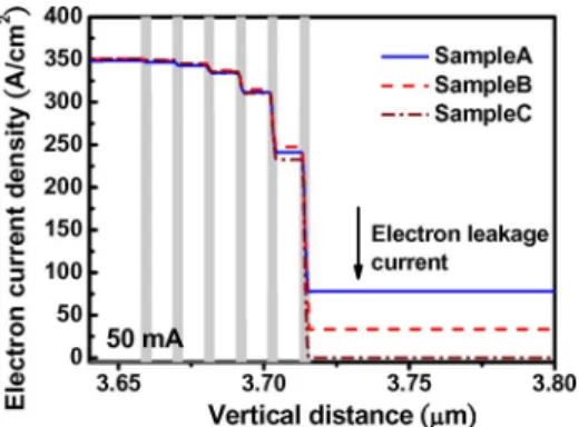
Fig. 4. Vertical electron current density profiles near the active regions of Sam-ples A, B, and C at 50-mA injection current.
the electron concentration in the p-type region can be effectively decreased by employing the p-type GaN last barrier, especially for Sample C with thick p-GaN last barrier. This situation can also be observed from the distribution of electron quasi-Fermi level shown in Fig. 2(c). Furthermore, the hole concentration near the p-side quantum well (QW) is higher in Samples B and C, as shown in Fig. 3(b), since the p-type GaN last barrier can provide higher hole concentration and then enhances the effec-tive hole injection into QWs.
Fig. 4 shows the vertical electron current density profiles near the active regions of these three LED samples when the input current is 50 mA. The electron current density and the elec-tron concentration are connected by the drift-diffusion model [12]. The positions of six QWs are marked with gray areas. The electron current is injected from n-type layers into QWs and re-combines with holes, which results in the decrease of electron current density. The electron current which overflows through QWs is viewed as leakage current. In Fig. 4, the electron leakage current is observed in Sample A. After inserting a p-type GaN layer, the electron overflow can be decreased significantly and the leakage current can be further suppressed by increasing the thickness of the p-type GaN last barrier from 25 to 75 nm. There-fore, the simulated output power of Sample C is slightly higher than that of Sample B at 50-mA injection current. Nevertheless, the measured output power of Sample C is slightly lower than that of Sample B. This inconsistency may be induced by the ab-sorption in the relatively thicker p-GaN layer in Sample C. Al-though the employment of a p-type GaN layer can decrease the electron overflow, the p-type AlGaN EBL is still necessary for GaN LEDs to endure the test of higher electrostatic discharge (ESD) levels [18].
IV. CONCLUSION
We have investigated the device performance of InGaN–GaN LEDs with different p-type GaN last barriers. The employment of a 25-nm-thick p-type GaN last barrier can improve the output power from 35.6 to 40.2 mW at 50 mA at RT. The further in-crease in the thickness of p-type GaN last barrier will give rise to a higher forward voltage. Consistent with simulation results,
an increase in the output power of the GaN LEDs with p-type GaN last barrier is confirmed through theoretical simulation. It is found that the electron overflow can be significantly sup-pressed after inserting the p-type GaN last barrier, which pro-vides a higher energy barrier by keeping the severe energy band bending away from the MQW region.
REFERENCES
[1] S. Nakamura and G. Fasol, The Blue Laser Diode. New York: Springer, 1997.
[2] A. Bell, R. Liu, F. A. Ponce, H. Amano, I. Akasaki, and D. Chems, “Light emission and microstructure of Mg-doped AlGaN grown on pat-terned sapphire,” Appl. Phys. Lett., vol. 82, p. 349, 2003.
[3] C. M. Tsai, J. K. Sheu, P. T. Wang, W. C. Lai, S. C. Shei, S. J. Chang, C. H. Kuo, C. W. Kuo, and Y. K. Su, “High efficiency and improved ESD characteristics of GaN-based LEDs with naturally textured sur-face grown by MOCVD,” IEEE Photon. Technol. Lett., vol. 18, no. 11, pp. 1213–1215, Jun. 1, 2006.
[4] C. H. Chiu, C. E. Lee, C. L. Chao, B. S. Cheng, H. W. Huang, H. C. Kuo, T. C. Lu, S. C. Wang, W. L. Kuo, C. S. Hsiao, and S. Y. Chen, “Enhancement of light output intensity by integrating ZnO nanorod arrays on GaN-based LLO vertical LEDs,” Electrochem. Solid-State
Lett., vol. 11, pp. H84–H87, 2008.
[5] A. David, T. Fujii, R. Sharma, K. McGroddy, S. Nakamura, S. P. Den-Baars, E. L. Hu, C. Weisbuch, and H. Benisty, “Photonic-crystal GaN light-emitting diodes with tailored guided modes distribution,” Appl.
Phys. Lett., vol. 88, p. 061124, 2006.
[6] M. F. Schubert, J. Xu, J. K. Kim, E. F. Schubert, M. H. Kim, S. Yoon, S. M. Lee, C. Sone, T. Sakong, and Y. Park, “Polarization-matched GaInN/AlGaInN multi-quantum-well light-emitting diodes with reduced efficiency droop,” Appl. Phys. Lett., vol. 93, p. 041102, 2008. [7] Y.-K. Kuo, J.-Y. Chang, M.-C. Tsai, and S.-H. Yen, “Advantages of blue InGaN multiple-quantum well light-emitting diodes with InGaN barriers,” Appl. Phys. Lett., vol. 95, p. 011116, 2009.
[8] N. Kuroda, C. Sasaoka, A. Kimura, A. Usui, and Y. Mochizuki, “Pre-cise control of pn-junction profiles for GaN-based LD structures using GaN substrates with low dislocation densities,” J. Cryst. Growth, vol. 189–190, pp. 551–555, 1998.
[9] S. Nakamura, T. Mukai, and M. Senoh, “In situ monitoring and Hall measurements of GaN grown with GaN bufferlayers,” J. Appl. Phys., vol. 71, pp. 5543–5549, 1992.
[10] J. Li, T. N. Oder, M. L. Nakarmi, J. Y. Lin, and H. X. Jiang, “Op-tical and electrical properties of Mg-doped p-type Al Ga N,” Appl.
Phys. Lett., vol. 80, pp. 1210–1212, 2002.
[11] V. Fiorentini, F. Bernardini, and O. Ambacher, “Evidence for nonlinear macroscopic polarization in III–V nitride alloy heterostructures,” Appl.
Phys. Lett., vol. 80, pp. 1204–1206, 2002.
[12] I. Vurgaftman and J. R. Meyer, “Band parameters for nitrogen-con-taining semiconductors,” J. Appl. Phys., vol. 94, pp. 3675–3691, 2003. [13] W. Götz, N. M. Johnson, J. Walker, D. P. Bour, and R. A. Street, “Acti-vation of acceptors in Mg-doped GaN grown by metalorganic chemical vapor deposition,” Appl. Phys. Lett., vol. 68, pp. 667–669, 1996. [14] J. Piprek and S. Nakamura, “Physics of high-power InGaN/GaN
lasers,” Proc. Inst. Elect. Eng., Optoelectron., vol. 149, pp. 145–151, 2002.
[15] Y. K. Kuo, S. H. Yen, and J. R. Chen, “Ultraviolet light-emitting diodes,” in Nitride Semiconductor Devices: Principles and
Simula-tion. Berlin, Germany: WILEY-VCH Verlag, 2007.
[16] D. Zhu, J. Xu, A. N. Noemaun, J. K. Kim, E. F. Schubert, M. H. Craw-ford, and D. D. Koleske, “The origin of the high diode-ideality fac-tors in GaInN/GaN multiple quantum well light-emitting diodes,” Appl.
Phys. Lett., vol. 94, p. 081113, 2009.
[17] J.-R. Chen, C.-H. Lee, T.-S. Ko, Y.-A. Chang, T.-C. Lu, H.-C. Kuo, Y.-K. Kuo, and S.-C. Wang, “Effects of built-in polarization and car-rier overflow on InGaN quantum-well lasers with electronic blocking layers,” J. Lightw. Technol., vol. 26, no. 3, pp. 329–337, Feb. 1, 2008. [18] C.-H. Jang, J. K. Sheu, C. M. Tsai, S. C. Shei, W. C. Lai, and S. J. Chang, “Effect of thickness of the p-AlGaN electron blocking layer on the improvement of ESD characteristics in GaN-based LEDs,” IEEE