Single-Mode 850 nm Vertical-Cavity Surface-Emitting Lasers with
Zn-diffusion and Oxide-relief Apertures for > 50 Gbit/sec OOK and
4-PAM Transmission
Jin-Wei Shi1*, Chia-Chien Wei2, Jason (Jyehong) Chen3, N.N. Ledentsov4 and Ying-Jay Yang5 1Department of Electrical Engineering, National Central University, Taoyuan 320, Tawian
*Tel: +886-3-4227151 ext. 34466, *FAX: +886-3-4255830 *Email: [email protected]
2Department of Photonics, National Sun Yat-sen University, Kaohsiung 804, Taiwan 3Department of Photonics, National Chiao-Tung University, Hsinchu 300, Taiwan
4VI Systems GmbH, Hardenbergstr. 7, Berlin 10623, Germany
5Department of Electrical Engineering, National Taiwan University, Taipei, 106, Taiwan
Abstract
Vertical-cavity surface-emitting lasers (VCSELs) has become the most important light source in the booming market of short-reach (< 300 meters) optical interconnect (OI). The next generation OI has been targeted at 56 Gbit/sec data rate per channel (CEI-56G) with the total data rate up to 400 Gbit/sec. However, the serious modal dispersion of multi-mode fiber (MMF), limited speed of VCSEL, and its high resistance (> 150 ) seriously limits the >50 Gbit/sec linking distance (< 10 m) by using only on-off keying (OOK) modulation scheme without any signal processing techniques. In contrast to OOK, 4-PAM modulation format is attractive for >50 Gbit/sec transmission due to that it can save one-half of the required bandwidth. Nevertheless, a 4.7 dB optical power penalty and the linearity of transmitter would become issues in the 4-PAM linking performance.
Besides, in the modern OI system, the optics transreceiver module must be packaged as close as possible with the integrated circuits (ICs). The heat generated from ICs will become an issue in speed of VSCEL. Here, we review our recent work about 850 nm VCSEL, which has unique Zn-diffusion/oxide-relief apertures and special p-doping active layer with strong wavelength detuning to further enhance its modulation speed and high-temperature (85℃) performances. Single-mode (SM) devices with high-speed (~26 GHz), reasonable resistance (~70 and moderate output power (~1.5 mW) can be achieved. Error-free 54 Gbit/sec OOK transmission through 1km MMF has been realized by using such SM device with signal processing techniques. Besides, the volterra nonlinear equalizer has been applied in our 4-PAM 64 Gbit/sec transmission through 2-km OM4 MMF, which significantly enhance the linearity of device and outperforms fed forward equalization (FFE) technique. Record high bit-rate distance product of 128 Gbps·km is confirmed for optical-interconnect applications.
Key words: Vertical-Cavity Surface-Emitting Lasers, Optical Interconnect, Green Photonics.
1. INTRODUCTION
To meet the strong demanding in construction of cloud infrastructure, optical interconnects (OIs) driven by vertical-cavity surface-emitting lasers (VCSELs) have been widely studied and envisioned as a promising solution [1-9]. As compared to its competitor: Si-photonic approaches for OI [10], VCSELs based solution usually has lower power consumption with lower cost and it has already dominated the market for very-short-reach (VSR) (< 300 meter) OIs [1-10]. To further enhance the modulation speed and reduce the cost of VCSELs are both important ways to meet the strong demand of bandwidth for next generation VSR-OIs in consumer electronics, such as, dual 4K display, 4K virtual reality display, and 4K 3600 video camera. Using multiple oxide layers with oxide aperture diameter less than 6 m is usually necessary to reduce the parasitic capacitance, increase the optical confinement, and enhance speed performance of VCSEL structures [1-3,9]. Through the use of these VCSELs, energy efficient >50 Gbit/sec transmission of 850 nm VCSEL has been demonstrated [3-5] for VSR linking distance (< 50 meter). However, the small current-confined aperture in these devices would usually result in large differential resistance (> 120 and impedance mismatch between VCSELs and driver ICs, which may degrade eye-patterns due to microwave reflections [11]. In addition, the high operation current density (~43.3 kA/cm2 [5]; ~25 kA/cm2 [1,2]) and the significant stress between multiple oxide layers and surrounding
from ICs will lead to an increase in the junction temperature of VCSEL and degrades its high-speed performance. To have an uncooled VCSEL for >50 Gbit/sec operation is thus highly desired to meet the low-cost requirement in the above-mentioned OI systems [12-14].
The other important issue in the development of VCSEL is to enhance its maximum error-free transmission distance under high-speed modulation. For the case of > 50 Gbit/sec OOK transmission through OM4 fiber, their maximum transmission distance is usually less than 10 meters due to their multi-mode output optical spectra and serious modal dispersion in MMF [3]. The digital signal processing (DSP) techniques is one effective way to overcome such bottleneck. A 64 Gbps 850nm VCSEL operation over 57 m OM4 MMF using two tap feed forward equalization was experimentally demonstrated [4,5], opening up the possibility of a higher bit rate with longer transmission distance by employing IC-based signal equalization. Nevertheless, the cost and power consumption of these ICs are both issues in these OI channels. To have a highly SM VCSEL with high-speed performance is thus desired to minimize the burden imposed on high-speed ICs for DSP and further enhance transmission distance at extremely high data rate (>50 Gbit/sec) [6,15]. Using an advanced modulation format onto VCSEL, such as 4- (or-8) PAM [16,17], is another promising solution to save the required bandwidth, minimize the modal dispersion, and enhance the transmission distance for the targeted data rate (> 50 Gbit/sec). However, the linearity of transmitter (VCSEL) thus becomes a major issue in such multi-level amplitude modulation schemes (PAM).
Here, we review our recent work about 850 nm VCSEL with Zn-diffusion/oxide-relief apertures and p-type doping active layers for further enhancing its modulation-speed, transmission distance, and high-temperature performances. Using such unique VCSEL structure with SM performance and signal processing techniques, error-free OOK transmission at 54 Gbit/sec data rate through 1 km OM4 MMF has been successfully demonstrated. Besides, the volterra nonlinear equalizer (VLNE) is proposed to effectively enhance the 64 Gbit/sec 4-PAM linking performance of our VCSELs through OM4 fiber. In spite of high computational complexity, as compared with equalizers for compensating linear distortion, such as feed-forward equalizer (FFE) and decision feed-back equalizer (DFE), Volterra nonlinear equalizer (VNLE) could effectively reduce the nonlinear distortion of optical transmission system. With VNLE, a record high bit-rate distance product of 128 Gbps·km (64 Gbps*2 km) is successfully demonstrated in the field of OIs communication using an 850-nm VCSEL and 2-km OM4 fiber, with the bit-error-ratio (BER) of 6.5×10⁻⁵ (below the FEC threshold of 1.8×10⁻⁴) [18].
2. DEVICE STRUCTURE
Figures 1 (a) and (b) show conceptual cross-sectional and top views of the studied device, respectively. With additional Zn-diffusion apertures in the top p-type DBR layers, we can not only manipulate the number of optical transverse modes inside VCSEL cavity but also reduce the differential resistance [7,8,19]. In addition, the oxide layer for current confinement is removed from our oxide-relief structure by using selective wet chemical etching [7,8,19] to reduce its parasitic capacitance [7,8,19]. The diameters of the Zn-diffusion (WZ) and oxide-relief apertures (Wo) of the measured devices are specified in the figures below. The fabricated device has a ~23 m diameter active mesa, which is integrated with the slot line pads for on-wafer high-speed measurement, as shown in Figure 1(b). The detail fabrication process can be referred to our previous work [7,8,19]. The epi-layer structure, purchased from LandMark1, is grown on a semi-insulating GaAs substrate, which is composed of three In0.1Ga0.9As/Al0.3Ga0.7As (40/80Å ) MQWs sandwiched between a 36-pair n-type and 26-pair p-type Al0.9Ga0.1As/ Al0.12Ga0.88As Distributed-Bragg-Reflector (DBR) layers with an Al0.98Ga0.02As layer (50 nm thickness) above the MQWs for oxidation. Compared with previous work [7,19], the thickness of the cavity layer has been further downscaled from 1.5 to 0.5 which shortens the internal carrier transit time [8]. Here, is the operating wavelength inside the VCSEL cavity. Due to the increase in the transit-time limited bandwidth, the low-frequency roll-off [19], which is usually the major bandwidth limiting factor of a single-mode VCSEL, can be minimized [8]. The Fabry-Perot (FP) dip mapping of the whole VCSEL wafer shows that the cavity resonant wavelength locates at around 860 nm and the detuning between the gain peak (839 nm) and FP dip (~860 nm) wavelengths is as large as around 20 nm. Such strong detuning would result in significant improvement in 3-dB O-E bandwidth of VCSEL due to the device self-heating induced red-shift of gain peak under high bias current [6,8,14].
Figure 1. (a) Conceptual cross-sectional views of demonstrated VCSELs. (b) Top-view of fabricated VCSEL chip. PMGI: polymethylglutarimide. (c) Measured 3-dB E-O bandwidths of VCSELs with two different oxide-relief apertures (black: ~3 m; red: ~5 m aperture sizes) under RT (solid symbols) and 85 ℃ (open symbols) operations.
3.
MEASUREMENT RESULTS
The light output and bias voltages versus current (L-I and V-I) characteristics of VCSELs with quasi-SM (Wo=3 m) and MM (Wo=5 m) performances are shown in Figures 2 (a) and (b), respectively. Both devices share the same geometric size (Wz, and d) except for Wo. Although it is doable to achieve highly SM performance in our device structure by choosing the size of W0 larger than Wz, which can induce significant intra-cavity loss and strongly suppress the higher order-modes [19]. However, this approach would degrade the maximum 3-dB E-O bandwidth of SM VCSEL [19]. Three typical measured traces (devices A to C and D to F) are shown in each figure. Thanks to our Zn-diffusion process, the measured differential resistance of devices A to C, even with such a small oxide-relief aperture, can be as low as 70~100 This is much smaller than the values typically reported (>150 for high-speed VCSELs at 850 nm with a similar size of current-confined aperture [2,3,11]. The L-I curves with solid and open symbols represent the measurement results at RT and 85℃ operation, respectively. We can clearly see that devices under 85℃ operation exhibit smaller threshold current than those of devices under RT operation. This can be attributed to the strong wavelength detuning in our VCSEL structure as discussed before.
Figure 2. Measured L-I-V curves of VCSELs with oxide-relief apertures of (a) 3m (devices A to C), (b) 5 m (devices D to F). The range of the measured differential resistance is specified on I-V curves. Solid and open symbols in L-I curves represent the measured power at RT and 85℃, respectively.
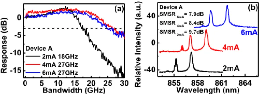
Thehigh-speed E-O performance of the fabricated devices was measured by a lightwave component analyzer (LCA), which was composed of a network analyzer (Anritsu 37397C) and a calibrated 25GHz photoreceiver module (New focus 1481-S). Figures 3 and 4 show the measured typical bias dependent E-O frequency responses and output optical spectra of devices A (quasi-SM) and D (MM), respectively under RT operation. We can clearly see that devices A and D shows a very close maximum 3-dB E-O bandwidth value at around 28 and 27 GHz, respectively. Furthermore, device A exhibits quasi-SM behavior with around 8 dB side-mode suppression ratio (SMSR) under 6 mA bias current. Here, the SMSR value of each trace of quasi-SM device is specified.
Undoped layer
Zn diffusion Pad
PMGI Oxide relief
SiO2 Active region P contact N contact WZ WO 220µm 220µm d (a) (b) 3 4 5 6 8 12 16 20 24 28 25O C 85O C B and w idth (G H z) Oxide Aperture (m) (c) 0 1 2 3 4 5 6 7 8 0.0 0.5 1.0 1.5 70~100 Power (mW) Current (mA) InGaAs 3m 25O C 85O C A B C 0 2 4 6 8 10 Voltage ( V) 50% 52% 0 1 2 3 4 5 6 7 8 9 0.0 0.8 1.6 2.4 50~80 Power (mW) Current (mA) InGaAs 5m 25O C 85OC D E F 0 2 4 6 8 10 Voltage( V) 57% 54% (a) (b)
Figure 3. (a) E-O frequency responses of device A (quasi-SM) measured under different bias currents and RT operation. (b) The corresponding bias dependent output optical spectra.
Figure 4. (a) E-O frequency responses of device D (MM) measured under different bias currents and RT operation. (b) The corresponding bias dependent output optical spectra.
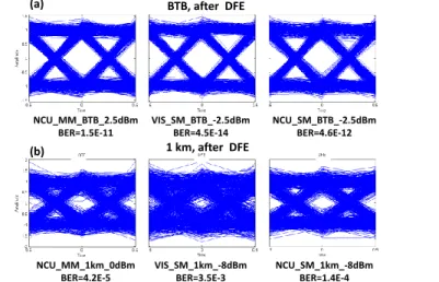
As shown in Figure 1 (c), the measured E-O bandwidths under RT operations of quasi-SM and MM devices range from 29-24 and 27-23 GHz, respectively. In addition, when the ambient temperature reaches 85℃, both devices have 3-dB bandwidths at around 16~18 GHz. Such distribution in device’s speed performance is mainly due to the process variation in oxide-apertures during mesa wet etching and oxidation. In addition, for the VCSEL structure we demonstrated here, there is a trade-off between SMSR and speed performance [19]. Our devices can have a perfect SM characteristic (SMSR> 30 dB) under the full range of bias current at the expense of a smaller 3-dB E-O bandwidth (~24 GHz), which will be discussed latter. Figure 5 (a) shows the measured received light output power vs. BER (after DFE process) of home-made SM (NCU_SM), MM (NCU_MM), and reference V50-850M (VIS_SM) devices measured at 54 Gbit/sec under back-to-back (BTB) and through 1 km OM4 fiber data transmission. Here, home-made device (NCU_SM) with a perfect SM performance but a slightly degraded 3-dB E-O bandwidth (~25 GHz) is chosen for this transmission experiment and it’s measured bias dependent output optical spectra with L-I-V curve is given in Figure 5 (b). We can clearly see that under full range of bias current, highly SM characteristic (SMSR>30 dB) can be sustained. The 54 Gbit/sec data rate adapted 50 Gbit/sec payload and 7% forward error correction (FEC) overhead. 54 Gbit/s non-return-to-zero (NRZ) electrical signal with pseudo-random binary sequence (PRBS) length of 215-1 is generated through SHF 12100B Bit Pattern Generator. All the devices are tested under the same peak-to-peak driving voltage (0.45 V) and the optimized bias current for lowest BER values of MM, SM, and V50-850 M is 6, 3, and 2 mA, respectively. The VCSELs under test are connected to an OM4 MMF with 1 km length. A photo-receiver module (New Focus; 1484-A-50) with a 22 GHz bandwidth and 80 V/W conversion gain is adopted in our receiving side. The output signal from receiver was captured in the Tektronix DPO 73304D real time oscilloscope for further offline signal processing. The offline processing involves signal resampling at twice the bit rate, synchronization and decision feedback equalization (DFE) with 40 T/2 forward taps and 10 feedback taps. The equalizer is trained with recursive least squares (RLS) algorithm using a training sequence consisting of 3900 first bits of the PRBS. Q-parameter is used for the calculation of BER. As shown in Figure 5 (a), for the case of 1 km transmission, BER values obtained for MM and two kinds of (quasi)-SM devices are all below FEC threshold (BER=3.8×10⁻³), therefore error-free 1 km transmission can be achieved once FEC and DFE are used. However, compared with the case of BTB transmission, there is a more serious power penalty in MM devices for error-free performance. This result indicates that modal dispersion instead of output power of VCSELs plays a more important role in determining the maximum possible transmission distance for such high data rate (54 Gbit/sec) [7]. Figure 6 (a) and (b) shows the corresponding eye diagrams of SM, MM VCESLs, and reference device (V50-850M) for the case of BTB and 1 km OM4 fiber transmission, respectively.
0 5 10 15 20 25 30 -15 -10 -5 0 (a) Respo nse (dB) Bandwidth (GHz) Device A 2mA 18GHz 4mA 27GHz 6mA 27GHz 855 858 861 864 -40 0 40 (b) Device A SMSR 6mA= 7.9dB SMSR 4mA= 8.4dB SMSR 2mA= 9.7dB 6mA 4mA Relati ve Inte nsit y (a.u. ) Wavelength (nm) 2mA 0 5 10 15 20 25 30 -25 -20 -15 -10 -5 0 5 (a) Respo nse (dB) Bandwidth (GHz) Device D 2mA 14GHz 4mA 22GHz 7.5mA 26GHz 858 860 862 864 -40 0 40 (b) Device D RMS 7.5mA= 0.97nm RMS 4mA = 0.71nm RMS 1.5mA= 0.52nm 7.5mA 4mA Relati ve Inte nsit y (a.u. ) Wavelength (nm) 1.5mA
(WE 2
,
So Of f o .5 Of101Baillaa.
Figure 5. (a) Received optical power vs. BER for MM and (quasi-)SM VCELs devices for BTB and over 1 km OM4 fiber transmission at 54 Gbit/sec. (b) The measured bias dependent output optical spectra of home-made highly-SM device chosen for transmission experiment. The inset shows its L-I-V curve.
Figure 6. Measured 54 Gbit/s eye diagrams (after DFE processing) of (quasi-) SM and MM VCSELs for (a) BTB and (b) through 1km OM4 fiber. Although we can attain high-performance 54 Gbit/sec transmission performance under RT operation, the measured E-O bandwidth shows significant degradation, which is around 35% (28 to 18 GHz) as shown in Figure 1 (c), when the ambient temperature reaches 85℃. In order to minimize the thermal induced degradation in speed performance, we have demonstrated the 850 nm VCSELs with p-type modulation doped in the barrier layers of highly strained active layer [20]. Compared with that of undoped reference, the p-doping device shows much faster modulation speed from RT to 85℃ operations. Furthermore, the p-doping devices shows superior L-I performance to that of undoped reference under 85℃ operation. Figures 7 shows the measured light output power (L) and bias voltage (V) versus current (L-V-I) characteristics observed at room-temperature (RT) and 85 ℃ for devices with/without p-type doping. In such figure, the traces are measured for two typical devices and their detail epi-layer structure is given in [20]. We can clearly see that the p-type doping devices exhibit a very close L-I-V performance compared to that of the reference sample without p-type doping, under RT operation. In contrast, when the ambient temperature reaches 85 ℃, the devices with p-type doping show the superior output power performance to the undoped device. This significant improvement in high-temperature (T) performance can be attributed to the fact that the electron quasi-fermi level in the p-doping device is closer to the conduction band minimum in the active region than in the undoped devices, which thus minimizes electron leakage and degradation in output power under high-T operation.
-12 -10 -8 -6 -4 -2 0 2 4 1E-15 1E-13 1E-11 1E-9 1E-7 1E-5 1E-3 0.1 NCU_MM_BTB NCU_MM_1km VIS_SM_BTB VIS_SM_1km NCU_SM_BTB NCU_SM_1km
BER after DFE
Received Optical Power (dBm)
FEC (a) (b) 845 850 855 860 865 -50 0 50 100 150 NCU SM SMSR 4mA= 33dB SMSR 2mA= 34dB SMSR 2mA= 34dB Relati ve Inte nsit y (a .u.) Wavelength (nm) 2mA 3mA 4mA 0 2 4 6 0.0 0.5 1.0 1.5 Vo ltag e (V) Po w er (m W ) Current (mA) 0 2 4 R = 140 I th = 0.76 mA NCU_MM_BTB_2.5dBm BER=1.5E-11 VIS_SM_BTB_-2.5dBm BER=4.5E-14 NCU_SM_BTB_-2.5dBm BER=4.6E-12
(a) BTB, after DFE
1 km, after DFE (b) NCU_MM_1km_0dBm BER=4.2E-5 VIS_SM_1km_-8dBm BER=3.5E-3 NCU_SM_1km_-8dBm BER=1.4E-4
Figure 7. Measured (a) L-I and (b) I-V curves of demonstrated devices under RT (solid symbols) and 85℃ (open symbols) operation with (black symbols) and without (red symbols) p-type modulation doping in the active MQWs. Wz/Wo/d=9/6/1 m.
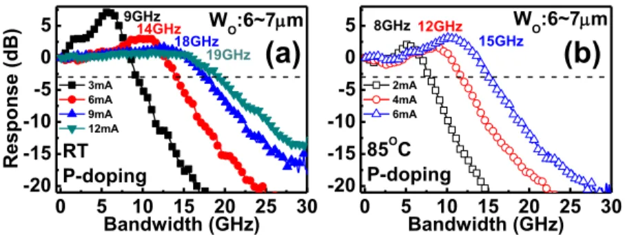
Figures 8 and 9 show the measured bias dependent electrical-to-optical (E-O) frequency responses (under RT and 85 ℃ operation) of devices with and without p-type doping, respectively. We can clearly see that even with the same oxide-relief aperture, the p-doping devices show significantly faster speed performance than the undoped ones, under both RT and 85 ℃ operation. The solid and open symbols in Figure 10 represent the summarized measured E-O bandwidth results for several p-doped and undoped devices, with three different oxide-relief diameters (~3, ~5, and ~7 m), under room-temperature (RT) and 85 ℃ operation, respectively. The values of measured 3-dB bandwidth shown in here is smaller than those shown in Figure 1 (c). This is because that the VCSELs, which have the measurement results as shown in Figures 8 to 10, have the 3/2 cavity design. This would lead to a smaller optical confinement factor and E-O bandwidths [3]. As can be seen, there is some variation in the measured 3-dB bandwidths with each aperture size, which can be attributed to variations in the process. These include uncertainty of the surface state during the p- and n-type ohmic contact metallization and uniformity during the wet oxidation processes. Nevertheless, there is a gradual improvement in the bandwidths of most devices with a downscaling of the size of the oxide-relief apertures. Furthermore, regardless of the aperture size, the p-type doped devices not only exhibit a faster modulation speed under RT operation but also show less degradation in the O-E bandwidth when the ambient temperature reaches 85 ℃ (~20 vs. ~40%) than those of the undoped ones.
Figure 8. Measured bias dependent electrical-to-optical (E-O) frequency responses of demonstrated devices with p-type modulation doping in the active MQWs under (a) RT (solid symbols) and (b) 85℃ (open symbols) operation. Wz/Wo/d=9/6/1 m.
Figure 9. Measured bias dependent electrical-to-optical (E-O) frequency responses of demonstrated devices with undoped active MQWs under (a) RT (solid symbols) and (b) 85℃ (open symbols) operation. Wz/Wo/d=9/6/1 m.
0 1 2 3 0 2 4 6 8 10
(b)
WO:6~7m RT 85OC P-doping Undoping Current (mA) Voltage (V) 0 2 4 6 8 10 12 14 16 0 1 2 3 4 5 6(a)
W O:6~7m RT 85OC P-doping Undoping Power (m W ) Current (mA) 68% 48%(a)
0 5 10 15 20 25 30 -20 -15 -10 -5 0 5 2mA 4mA 6mA 9mA(a)
WO:6~7m RT Undoping Respo nse (dB) Bandwidth (GHz) 16GHz 7GHz11GHz14GHz 0 5 10 15 20 25 30 -20 -15 -10 -5 0 5 2mA 4mA 6mA WO:6~7m(b)
85OC Undoping Bandwidth (GHz) 6GHz 9GHz 9GHz 2 3 4 5 6 7 8 10 12 14 16 18 20 22(a)
P-doping 25OC 85OC B and w idth (G H z) Oxide Aperture (m) 4 5 6 7 8 9 8 10 12 14 16 18 20 22(b)
Oxide Aperture (m) 25OC 85OC Undoping 40% 37% 39% 24% 19% 20%Figure 10. Measured 3-dB E-O bandwidths of VCSELs (a) with and (b) without p-type modulation doping of the active layers for different oxide-relief apertures under RT (solid symbols) and 85 ℃ (open symbols) operation. The Wz/d of all the measured devices is fixed at 9/1 m.
As above discussion, 8×50 Gbps solution will soon be considered as a standard for 400 Gbps linking due to its smaller footprint and power consumption as compared to those of 16×25 Gbps approach. Two possible modulation formats are NRZ and 4-PAM. NRZ has simpler electronic driving circuit that can use a limiting amplifier to reduce the nonlinearity stems from the temperature-dependent transfer curve, and it also has better receiving power sensitivity. Nonetheless, compared with 4-PAM format, NRZ requires higher modulation bandwidth that will undoubtedly increase the cost of the system and induce more serious modal dispersion. On the other hand, with about only half bandwidth requirement of NRZ, 4-PAM format suffers the modulation penalty of about 4.7 dB and requires better linearity because four different levels are needed. However, the 4-PAM may better reach the higher data rates for next-generation applications. To date, 4-PAM 70-Gbps transmission using an 850 nm VCSEL has been realized, but the transmission length of MMF is only 3 m, even with offline equalization[21]. More recently, 4-PAM 51.56-Gbps per channel transmission over 150 m MMF has been demonstrated in an SWDM system [22]. The limited linear operational region of VCSELs is one of the major challenges in applying the 4-PAM format because it may cause nonlinear distortion in a short-reach 850 nm 4-PAM transmission system. In spite of high computational complexity, as compared with equalizers for compensating linear distortion, such as feed-forward equalizer (FFE) and decision feed-back equalizer (DFE), Volterra nonlinear equalizer (VNLE) may effectively reduce the nonlinear distortion of optical transmission system [18]. The
m
thsample of the output signal waveform of the VNLE can be expressed as following:) ( ) ( ) ( 1 1 1 0 1 1 l m x l w n y L l
2 1 1 0 1 0 2 1 2( , ) ( ) 1 2 i i L l L l l m x l l w
k i i L l L l L l k k l l l xm l w 1 1 0 1 0 1 0 2 1, ,..., ) ( ) ( 1 2 3(1)
Where x(m-l1) is the (m-l1)th sample of the received signal, wk(l1, l2,…lk) is the weighting factor of the kth order, and L is the
tap number. The 1st term of Eq. (1) indicates a linear filter and the others are nonlinear filters. If we only consider 1st term of VNLE, the performance should similar to FFE and DFE. This experiment has taken into consideration two cases: the 2nd-order and 3rd-order Volterra filtering. To limit the computational complexity of VNLE, we ignore the nonlinear terms higher than 2nd order and 3rd order, respectively. Besides, only the 3rd-order terms of l
1=l2=l3 are included in the 3rd-order
filtering to reduce the complexity; thus, extra complexity of the 3rd-order terms will be linearly proportional to 𝐿. The weighting factors are determined by the Wiener solution, in which the required expectation values are replaced by sample means of training symbols.
Figure 11 shows the experimental transmission setup. The electrical signal is generated by Anritsu® MP1800A Signal Quality Analyzer. Two independent pseudo-random-binary-sequence 7 (PRBS15) NRZ signals at 32 Gbps are generated and sent into the MZ1834A 4-PAM converter, which converts the two NRZ signals to one 4-PAM signal. Then, the 4-PAM signal is fed into the VCSEL through a 26.5-GHz bias-T (Agilent 11612A) and a GS probe. The output light is butt-coupled
0 5 10 15 20 25 30 -20 -15 -10 -5 0 5 3mA 6mA 9mA 12mA
(a)
WO:6~7m RT P-doping Respo nse (dB) Bandwidth (GHz) 19GHz 9GHz 14GHz 18GHz 0 5 10 15 20 25 30 -20 -15 -10 -5 0 5 2mA 4mA 6mA WO:6~7m(b)
85OC P-doping Bandwidth (GHz) 8GHz12GHz 15GHzjIW6 (b2) -0'4 0 E. 0A 0'S 0 40 SO 30 40 20 1a
-44110`
00 {j6C61A6Q ET6 o -01 41 0 E 0'4 0121WPOI Ot polowEø 91/3 b9vi9o9A oa oa oD OE OS or (aq) mil (IWG (t2) JO so 30 do 20 eo
EAeqpsBLsw ot psFs 9E4et Ao)
03 91019d sJsa ìo Iodmya ','<gX a.r e.o o a.o- r- a.r r a.o o (aq) 9miJ pwe (ba) 3 3 ZÀwPOi Ot p949 9((6L AO(
loV lefls sisa To msigsibe \3 /o-_.=. `, 00 OZ OP oc OS or 0 Z-(29) omit pun (b2) x40. 0'2 d 4'2 S 2AwP0)Dé Dg(g 8(161 AO)
signal, before measuring signal-to-noise ratio (SNR) and BER. We measured the BER by two ways: the Q-factor of eye diagram (BER-Q) and error count via bit-by-bit comparison (BER-count).
Figure 11. Experimental transmission system.
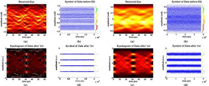
It should be noted that, in order to enjoy the large modulation bandwidth of our VCSEL without sacrifice of modulation efficiency, we overdrive driving-voltage range to non-linear region of L-I curve with a bias current of 9 mA, and the resulted nonlinear distortion will be compensated by the VNLE. Fig. 12 shows experimental results of 64 Gbps 4-PAM at optical back-to-back (OBTB), and Fig. 13 shows results after 2-km OM4 MMF. The left columns of Figs. 12 and 13 exhibit the eye diagrams, and the right columns plot amplitudes at the decision instants and their corresponding histogram. In Figs. 12 (a) and (b), no equalization is applied, and the BER is about 3.4×10⁻². Figs. 12 (c) and (d) show the experimental results after employing the VNLE, and the VNLE significantly improves the transmission performance with the BER of far below 10-12. The impairment compensated by the VNLE is mainly composed of the linear inter-symbol interferences (ISI) and nonlinear distortion, which are respectively caused by the limited bandwidth of photo-receiver and over-driving operation of VCSEL, in the OBTB case. The results after 2-km OM4 fiber are shown in Figs. 13 (a)-(d). Without the VNLE, the estimated BER in Figs. 13 (a) and (b) is 0.13. After applying the VNLE, as show in Figs. 13 (c) and (d), the performance is significantly improved, and BER is lowered to about 6.5×10⁻⁵, which is below the FEC threshold of 1.8×10⁻⁴. This implies that the MMF-induced ISI and nonlinearity are also effectively compensated by the VNLE, making it possible to realize the record high bit-rate distance product of 128 Gbps·km.
(a) (b) (c) (d) (a) (b) (c) (d) Bias Tee VCSEL Tx 2-km OM4 Fiber Photo receiver VOA D e m o d u la ti o n V o lt e rr a F il te r
Amp: Amplifier; VOA: Variable Optical Attenuator
Rx MZ1834A 4PAM Converter 32 Gbps Pattern generator MP1800A 32 Gbps Power Supply Tektronix MSO73304DX Mixed Signal Oscilloscope
Offline DSP
Amp.
Fig. 12 4-PAM performance at OBTB: (a) eye diagram and (b) amplitude distribution and histogram of decision points before equalization, and (c) eye diagram and (d) amplitude distribution and histogram of decision points after the VNLE.
Fig. 13 4-PAM performance after 2-km OM4 fiber: (a) eye diagram and (b) amplitude distribution and histogram of decision points before equalization, and (c) eye diagram and (d) amplitude distribution and histogram of decision points after the VNLE.
4. CONCLUSIONS
By using Zn-diffusion and oxide-relief structures, high-performance single-mode 850 nm VCSELs for > 50 Gbit/sec transmission through 1 km OM4 fiber have been successfully demonstrated. Compared with the reported multi-oxide VCSELs, our unique device structure can greatly enhance the modulation speed, improve device reliability, control the output optical spectra, and reduce the differential resistance (impedance) of device. All these issues play vital roles in the application of > 50 Gbit/sec transmission. Besides, by incorporating the p-type doping in the active layers of our VCSELs structures, the degradations in modulation speed and output power performances under high-temperature operation (85℃) can be effectively minimized. In order to enhance the linearity for 64 Gbit/sec 4-PAM transmission by use of our device, VLNE technique has been firstly demonstrated in the VSR OI linking at 850 nm wavelength. The 2-km MMF transmission experimentally shows BER of ~6.5×10⁻⁵ after applying the VNLE, which fits the requirement of FEC, demonstrating the record high bit-rate distance product of 128 Gbps·km.
REFERENCES
[1] P. Moser, P. Wolf, G. Larisch, H. Li, J. A. Lott, and D. Bimberg, “Energy-efficient oxide-confined high-speed VCSELs for optical interconnects,” Proc. SPIE, Vertical-Cavity Surface Emitting Lasers XVIII, vol. 9001, pp. 900103, Feb., 2014.
[2] P. Westbergh, R. Safaisini, E. Haglund, J. S. Gustavsson, A. Larsson, M. Geen, R. Lawrence, and A, Joel, “High-Speed Oxide Confined 850-nm VCSELs Operating Error-Free at 40 Gb/s up to 85℃,” IEEE Photon. Technol. Lett., vol. 25, pp.768-771, April, 2013.
[3] E. Haglund, P. Westbergh, J.S. Gustavsson, E.P. Haglund, A. Larsson, M. Geen, and A. Joe, “30 GHz bandwidth 850 nm VCSEL with sub-100 fJ/bit energy dissipation at 25-50 Gbit/s,” Electron. Lett., vol. 51, no. 14, pp. 1096-1098, July, 2015.
[4] D. M. Kuchta, A. V. Rylyakov, F. E. Doany, C. L. Schow, J. E. Proesel, C. W. Baks, P. Westbergh, J.S. Gustavsson, and A. Larsson, “A 71-Gb/s NRZ Modulated 850-nm VCSEL-Based Optical Link,” IEEE Photon. Technol. Lett., vol. 27, pp.577-580, March, 2015.
[5] D. M. Kuchta, A. V. Rylyakov, C. L. Schow, J. E. Proesel, C. Baks, P. Westbergh, J. S. Gustavsson, and A. Larsson, “64Gb/s Transmission over 57m MMF using an NRZ Modulated 850nm VCSEL,” Proc. OFC 2014, San Francisco, CA, USA, March, 2014, pp. Th3C. 2.
[6] Kai-Lun Chi, Yi-Xuan Shi, Xin-Nan Chen, Jason (Jyehong) Chen, Ying-Jay Yang, J.-R Kropp, N. Ledentsov Jr., M. Agustin, N.N. Ledentsov, G. Stepniak, J. P. Turkiewicz, and Jin-Wei Shi, “Single-Mode 850 nm VCSELs for 54 Gbit/sec On-Off Keying Transmission Over 1 km Multi-Mode Fiber,” IEEE Photon. Technol. Lett., vol. 28, no. 12, pp. 1367-1370, June, 2016.
[7] Jin-Wei Shi, Jhih-Cheng Yan, Jhih-Min Wun, Jason (Jyehong) Chen, Ying-Jay Yang, “Oxide-Relief and Zn-Diffusion 850 nm Vertical-Cavity Surface-Emitting Lasers with Extremely Low Energy-to-Data-Rate Ratios for 40 Gbit/sec Operations” IEEE J. of Sel. Topics in Quantum Electronics, vol. 19, pp. 7900208, March/April, 2013.
[8] Kai-Lun Chi, Jia-Liang Yen, Jhih-Min Wun, Jia-Wei Jiang, I-Cheng Lu, Jason (Jyehong) Chen, Ying-Jay Yang, and Jin-Wei Shi, “Strong Wavelength Detuning of 850 nm Vertical-Cavity Surface-Emitting Lasers for High-Speed (>40 Gbit/sec) and Low-Energy Consumption Operation,” IEEE J. of Sel. Topics in Quantum Electronics, vol. 21, no. 6, pp. 1701510, Nov.,/Dec., 2015.
[9] J.-R. Kropp, V. A. Shchukin, N. N. Ledentsov, Jr., G. Schaefer, N. N. Ledentsov, B. Wu, Q. Shaofeng, M. Yanan, F. Zhiyong, and J. P. Turkiewicz, “850 nm single mode VCSEL-based 25Gx16 transmitter/receiver boards for parallel signal transmission over 1 km of multimode fiber,” Proc. SPIE, Next-Generation Optical Networks for Data Centers
and Short-Reach Links II, vol. 9390, pp. 93900C, March, 2015.
[10] M. A. Taubenblatt, “Optical Interconnects for High-Performance Computing,” IEEE/OSA Journal of Lightwave
Technology, vol. 30, No. 4, pp. 448-458, Feb., 2012.
[11] P. Westbergh, R. Safaisini, E. Haglund, B. Kogel, J. S. Gustavsson, A. Larsson, M. Geen, R. Lawrence, and A, Joel, “High-Speed 850 nm VCSELs with 28 GHz modulation bandwidth operating error-free up to 44 Gbit/s,” Electron.
Lett., vol. 48, no. 18, Aug., 2012.
[12] D. M. Kuchta, A. V. Rylyakov, C. L. Schow, J. E. Proesel, C. W. Baks, P. Westbergh, J.S. Gustavsson, and A. Larsson, “A 50 Gb/s NRZ Modulated 850 nm VCSEL Transmitter Operating Error Free to 90 °C,” IEEE/OSA Journal of
Transmission Operating up to 85 °C,” in Technical Digest of Conference on Lasers and Electro-Optics, paper SF1L.6, San Jose, CA, USA, May 2016.
[14] H. Li, P. Wolf, P. Moser, G. Larisch, A. Mutig, J. A. Lott, and D. H. Bimberg, “Impact of the Quantum Well Gain-to-Cavity Etalon Wavelength Offset on the High Temperature Performance of High Bit Rate 980-nm VCSELs,” IEEE J.
Quantum, Electron., vol. 50, pp. 613-621, Aug., 2014.
[15] G. Stepniak, A. Lewandowski, J.R. Kropp, N.N. Ledentsov, V.A. Shchukin, N. Ledentsov Jr., G. Schaefer, M. Agustin and J.P. Turkiewicz, “54 Gbit/s OOK transmission using singlemode VCSEL up to 2.2 km MMF,” Electron. Lett., vol. 52, no. 8, pp. 633-635, April, 2016.
[16] K. Szczerba, P. Westbergh, J. Karout, J. S. Gustavsson, Å . Haglund, M. Karlsson, P. A. Andrekson, E. Agrell, and A. Larsson, “4-PAM for High-Speed Short-Range Optical Communications,” J. Opt. Comm. Netw., vol., 4, pp. 885-894, Nov., 2012.
[17] J. M. Castro, R. Pimpinella, B. Kose, P. Huang, B. Lane, K. Szczerba, P. Westbergh, T. Lengyel, J. S. Gustavsson, A. Larsson, and P. A. Andrekson, “Investigation of 60 Gb/s 4-PAM Using an 850 nm VCSEL and Multimode Fiber,”
IEEE/OSA Journal of Lightwave Technology, vol. 34, no. 16, pp. 3825-3836, Aug., 2016.
[18] Jun-Jie Liu, Kai-Lun Chi, Chia-Chien Wei, Tien-Chien Lin, Chun-Yen Chuang, Xin-Nan Chen, Jin-Wei Shi, and Jyehong Chen, “Transmission over 2-km OM4 fiber Using an 850-nm VCSEL and a Volterra Nonlinear Equalizer,”
Proc. OFC 2017, Los Angeles, CA, USA, March, 2017, pp. W3G.5.
[19] Jin-Wei Shi, Zhi-Rui Wei, Kai-Lun Chi, Jia-Wei Jiang, Jhih-Min Wun, I-Cheng Lu, Jason (Jyehong) Chen, and Ying-Jay Yang, “Single-Mode, High-Speed, and High-Power Vertical-Cavity Surface-Emitting Lasers at 850 nm for Short to Medium Reach (2 km) Optical Interconnects,” IEEE/OSA Journal of Lightwave Technology, vol. 31, pp. 4037-4044, Dec., 2013.
[20]Kai-Lun Chi, Dan-Hua Hsieh, Jia-Liang Yen, Xin-Nan Chen, Jason (Jyehong) Chen, Hao-Chung Kuo, Ying-Jay Yang, and Jin-Wei Shi, “850 nm VCSELs with P-type 𝛅-Doping in the Active Layers for Improved Speed and High-Temperature Performance,” IEEE J. of Quantum Electronics, vol. 52, pp. 2400607, Nov., 2016.
[21] K. Szczerba, P. Westbergh, M. Karlsson, P. A. Andrekson, A. Larsson, “70 Gbps 4-PAM and 56 Gbps 8-PAM using an 850 nm VCSEL,” Proc. ECOC, Cannes, France, 2014, pp. Tu.4.3.4.
[22] J. M. Castro, R. Pimpinella, B. Kose, Y. Huang, B. Lane, A. Amezcua, M. Bigot, D. Molin, and P. Sillard, “200m 2x50 Gb/s PAM-4 SWDM Transmission Over Wideband Multimode Fiber using VCSELs and Pre-distortion Signaling,”