M04B-5
A
5.8-GHz
Two-Stage High-Linearity Low-Voltage Low Noise
Amplifier in a
0.35-pm CMOS
Technology
Ren-Chieh Liu, Chung-Rung Lee, Huei Wang and Chomg-Kuang Wang
Dept. of Electrical Engineering, National Taiwan University
Taipei, Taiwan, Republic of China
Abstract
- A 5.8-GHz two-stage high-linearity low-
voltage CMOS low-nose ampliner (LNA) has been developed in a 0.35-pm pure digital CMOS technology without any additional mask or post-processing steps. A two-stage architecture is used to simultaneously optimize the gain and noise performance. Based on the modified CMOS model valid for RF range, the LNA with fully on-chip input, output and inter-stage matching was designed to verify the two-stage LNA architecture. This LNA chip achieves measured results of 3.2-dB NF, +6.7-dBm IIP3 and -3.7-dBm output PldB at 5.8 GHz. A figure-of-merit for linearity (output IP3/PDc) of 1.2 is achieved, which is believed to be among the best reported for a CMOS low-noise amplifier operating at 5-6 GHz ISM band.
The effective circuit area is only 0.63 x 0.46 mm’.
I. INTRODUCTION
The demand on high bit-rate wireless LAN systems is driven by the growing popularity of notebook computers.
To provide data rates of several tens of megabits per second in wireless LAN systems, OFDM based WLAN modulation in the 5-6 GHz ISM band becomes very popular. OFDM based WLAN modulation is very challenging to RF front-end circuits about the linearity and dynamic range. Besides, to operate in wideband wireless portable systems, low-voltage low-power RF circuits are required. The design of such circuits is therefore a key
issue and LNA is the most important component in the receiver chain.
LNAs using high performance processes were designed [1]-[7]. However, due to the advantages of low cost and integration ability with baseband circuits, the CMOS RF
chips are getting more and more attractive. LNAs using 0.24-pm CMOS processes have demonstrated good gain and noise performance in the 5-6 GHz ISM band [8]. To achieve such performance, however, a costly RF-enhanced CMOS process is required and the power consumption and the power supply requirement are very large. A 2V LNA using 0.24-pm CMOS process with 7.2-mW power consumption [9] and an LNA using 0.35-pm CMOS process [IO] were designed but the noise performance is
degraded seriously. An alternative low-voltage topology using a planar-interleaved transformer was depicted using 0.35-pm CMOS process [ I l l . However, the low-Q transformer contributes significant resistance in the RF
range, which not only reduces the gain but also increases the noise figure (NF). Besides, the linearity is degraded due to the use of the cascode architecture in the previous circuits. In this paper, to simultaneously achieve high performance, high linearity, low supply voltage, low power consumption, a 5.8-GHz two-stage low-nose
Table. 1. Recently reported performance of 5-6GHz ISM band low noise amplifiers. Effective circuit areas without pads are estimated from the die photograph. (CC: Cascode topology. CS: Common-source topology. CE: Common-emitter topology).
0-7803-7246-8/02/$10.00 0 2002 IEEE
22 1
amplifier architecture was designed in a 0.35-pm pure digital CMOS technology without any additional mask or
post-processing steps. Table 1 summarizes the recently reported performance of 5-6 GHz ISM band low noise amplifiers compared with this work. Our chip demonstrated the best output IP3/PDc with a miniature effective chip size among the previous reported CMOS LNAs at this frequency.
11.5.8-GHZ TWO-STAGE LNA CIRCUIT DESIGN The performance of the sensitivity of a communication system is heavily determined by a LNA. A system noise figure is defined as
where F,, Fz, F3,
...
is the noise factor of each stage,GI,
G2,
G,,
. . .
is the gain of each stageThe typical CMOS LNA circuit topology is cascode with the inductor degeneration. Since the drain of the common-source stage is terminated with the source of the common-gate stage, the gain of the common-source stage is relatively small and the total noise performance will be degraded by the noise of the common-gate stage according to ( 1 ) . Besides, the unit-gain frequency of the device
depends on not only the overdriving voltage (V,
-
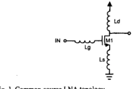
V,) but also drain-source voltage (VdS). To provide enough unit- gain frequency to achieve noise and gain performance, higher value of V, and V b are needed, which not only increases the supply voltage (Vdd) but also degrades the linearity.Fig. 1. Common-source LNA topology.
1
Z,, = s ( L , + L , ) + - + R , + R ,
+R,
+ k L , (2) where Cgs is the gate-source capacitance and g,,,, is the transconductance of device M1. Rg is the effective gateresistance. RLg and R h are the parasitic resistance of the inductors Lg and L, and are approximately proportional to
Lg and L,, respectively. The matching condition occurs when
sc,
c,,
O*C,,(L, + L , ) = l (3)
R, = R,
+
R ,+
R ,+
L, (4)CP
where o is the center frequency in radiansk With these conditions, the LNA noise factor F can be show to be
where gdo is the zero-bias drain conductance of the device, and y is a bias-dependent factor [ 131.
The noise figure of LNA becomes high value when the value of
Lg
is increases. Besides, because the spiral inductor is not ideal, the parasitic resistance of the inductor will degrade the noise figure. Hence, based on (1)-(3), it is hard to simultaneously optimize gain and noise performance with constrained power consumption.A two-stage topology is used to simultaneously optimized the gain and noise performance as in Fig.
2.
The first stage is designed for noise performance and the second stage is designed for gain. The maximum power gain is obtained whenr,
=rm*
andrL
=rout*
with the- inductors L,, L@d and L,. The two slage are complex conjugate matched by the interstage inductor L,.'
To achieve high linearity, low supply voltage, and avoid noise performance degradation, a common-source topology is adopted as in Fig. 1 . The input matching
condition and noise performance of an inductor- degeneration topology with ideal inductors was hlly analyzed in [12]. Due to the IOW Q of the inductors in the 0.35-pm CMOS technology, the parasitic resistance has to be considered. The input impedance is
c-
alas- I
-
Fig. 2. Proposed topology of two-stage low-voltage CMOS LNA. On-chip decoupling capacitor cds is used as a RF-short in the VDD to filter out the high frequency power supply noise and to rid of the influence of the parasitic inductance
of the bonding wire or the DC probe. 200w0.35p.m and lOOp1d0.35p.m MOSFETs are used in the first and second stages respectively for the power consumption consideration. Due the high sheet resistance of poly gate of the MOSFET, a multi-finger structure with 5p.m finger length was used in each MOSFET to reduce the gate resistance such that
Rg
in ( 5 ) can be reduced and the noise performance could be improved.111. RF.MoDELs AND LAYOUT CONSIDERATION The modified MOSFET model for simulation is based on the BSIM3v3 SPICE model, with some passive components added to take account of the parasitic effects in the RF range. Besides, although RF-enhanced CMOS processes provide a thick top metal to enhance the Q- factor of the spiral inductor and a thin oxide layer to increase the value of the capacitor, these needs a additional masks and are not standard processes for pure digital CMOS.
The inductors were modeled as a lump-circuit network and the parameters were extracted by experimental measurements. The Q-factor of on-chip spiral inductor is quite low due to its parasitic effects. In order to reduce the loss in the metal conductance of a spiral inductor, a hollow spiral inductor is used to increase the value of Q [ 141 and the top three metal layers are shunted to reduce parasitic resistance of the inductor as in Fig. 3.
Fig. 3. The top three metal layers are shunted to reduce the parasitic resistance of the inductor.
The large decoupling capacitor was designed with a interleaved metal capacitor instead of a MOS capacitor due to noise and linearity consideration as in Fig. 4, and the spare area was made full use of to reduced area. To prevent unexpected stability problems and noise,
all
blank area was covered with fully connected “ground” but the neighborhood of the passive and active devices to reduce extra parasitic effects.The layouts of all devices remain the same as the test keys to coincide with the measurement. For accuracy, the
parasitic effect of each interconnection was carefully aalculated and included in the post-layout simulation.
Fig. 4. The decoupling capacitor was constructed with interleaved metals.
Iv.
MEASUREMENT RESULTSThe proposed two-stage low-voltage CMOS LNA was fabricated using a 0 . 3 5 - p 1P4M standard digital CMOS process, which provides single poly layer for the gates of the MOS and four metal layers for interconnection. A die micrograph is shown in Fig. 5 . The chip size is 0.88x0.74
mm2 and the effective circuit area without pads is only 0.63~046 mm2. The circuit was tested via on-wafer probing. Fig. 6 shows the measured S-parameters and noise figure. The measured values were as follows: IS 11
I
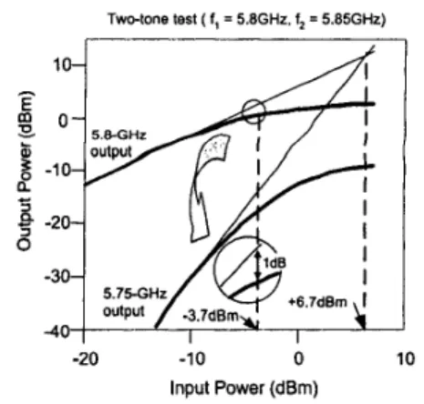
is -1 ldB, IS221 is -17dB, IS211 is 7.2dB and NF is 3.2dB at 5.8 GHz, with 15mA drawn form the 1.3V supply voltage without any off-chip tuning. The measurement result of a two-tone third order intercept point (IP3) with 5.8-GHz and 5.85-GHz inputs was showed as in Fig. 7. The input-referred IP3 is +6.7dBm and the measured input-referred PldB is -3.7dBm. The relatively low gain performance of the LNA is due to the on-chip low-Q spiral inductors and the tradeoffs of bias for low noise and dc power consumption.V. CONCLUSION
A two-stage high-linearity low-voltage low-noise amplifier topology using low-cost 0.35-pm CMOS process has been demonstrated. This 1.3V 5.8-GHz CMOS LNA has been designed, fabricated and tested. The measurement results prove that the proposed CMOS LNA topology can achieve the demand of low noise and high linearity with low supply voltage at a high frequency. Since this LNA was fabricated using standard 0.35-pm CMOS technology, it can be easily integrated with other front-end circuits to built CMOS transceivers without requiring any additional mask or post-processing steps.
ACKNOWLEDGEMENT
This work is supported in part by National Science
Council, ROC
(contact no.
NSC 89-2213-E-002-178, NSC89-22 19-E-002-042) and the Research Excellence Program funded by Ministry of Education, ROC (ME 89- E-FA06-2-4). The chip is fabricated by TSMC through the
Chip Implementation Center (CIC), Taiwan, ROC. The authors would like to thank K. L. Deng, P. Y. Chen and National Nano-Device Laboratory (NDL), Taiwan, ROC,
for the chip testing. Thanks also go to Prof. Y. J. Chan of National Central University for providing CMOS RF models.
Fig. 5. Die photograph ofproposed two-stage CMOS LNA.
REFERENCES
U.
z
[ 11 Urs Lon, “Low dc power monolithic low noise amplifier for wireless application at 5 GHz,” IEEE Millimeter- Wave
Monolithic Circuit Symp., pp. 81-84, June 1996
[2] K. W. Kobayashi, A. K. Oki, L. T. Tran, and D. C. Streit, “Ultra-low dc power GaAs HBT S- and C-band low noise amplifiers for portable wireless applications,” IEEE Tran. on MT7, vol. 43, no. 12, Dec. 1995
M. Soyuer, J-0. Plouchart, H. Ainspan, and J. Burghartz, “A 5.8-GHz I-V low-noise amplifier in SiGe bipolar Technology,”IEEE RFICSymp., pp. 19-21, 1997
S. P. Voinigescu, and M. C. Maliepaard, “5.8GHz and 12.6GHz Si bipolar MMICs,” ZEEE ISSCC97 Dig. Tech.
Papers, pp. 372-373, 1997
G. Schuppener, M. Mokhtari, and B. Kerzar, “A 5.8 GHz low noise amplifier for wireless Ian applications in silicon bipolar technology,” Proceedings of ICECS, Vol. 2., pp. M. Ono, N. Suematsu, S. Kubo, Y. Iyama, T. Takagi, and 0. Ishida, “1.9GHd5.8GHz-band on-chip matcing Si-MMIC low noise amplifiers fabricated on high resistive Si substrate,” IEEE RFIC Symp., pp. 189-1 92, 1999 T. K. K. Tsang and M. N. El-Gamal, “A fully integrated 1V
5.8 GHz bipolar LNA,” ZEEE ISCAS, pp. 842-845, 2001 Eric H. Westerwick, “A 5GHz band CMOS low noise amplifier with a 2.5dB noise figure,” Symp. On VLSI Tech.
Sys. and App., pp. 224-227,2001
Hirad Samavati, Hamid R. Rategh, and Thomas H. Lee, “A
SGHz
CMOS
wireless LAN receiver front end,” IEEE J.Solid-State Circuits. vol. 35. no. 5. DD. 765-772. Mav 2000 773-776,1999
4 5 6 7 8
Frequency ( GHz )
Fig. 6. Measurement results of proposed two-stage CMOS LNA.
0 S21 (IS211 = 7.2dB at 5.8GHz) A S11 (IS1 11 = -1 1dB at 5.8GHz)
o
S22 (IS221 = -17dB at 5.8GHz) x Noise Figure (NF = 3.2dB at 5.8GHz) Two-tone test ( 1, = 5.8GHZ. f, = 5.85GHz) -3 - 1
1
[IO] K. Runge, D. Pehlke and B.’Schiffei: “On-chip matdhed 5.2 and 5.8 GHz differential LNAs fabricated using 0.35” CMOS technology,” Electron. Lett., vol. 35, no. 22, pp.
low-noise amplifier using planar-interleaved transformer,”
Electron. Lett., vol. 37, no. 8, pp. 497-498, April 2001 CMOS low noise amplifier”, IEEE J. Solid-state Circuits,
vol. 32, no. 5, pp. 745-759, May 1997
[I31 A. van der Ziel, “Thermal noise in field effect transisteors,”
Proc. IEEE, pp. 1801-1812, Aug. 1962
[14] Q. Huang et al., ‘The impact of scaling down to deep submicron on CMOS RF circuit’, ZEEE J. Solid-Sfate Circuits, vol. 32, no. 5, pp. 2071-2088, 1997
0
1899-1 900, April 1999 -30
+6.7dBm I [ 111 Chin-Chun Tang, and Shen-Iuan Liu, “Low-voltage CMOS 5.75-GHz
Output -3.7dBm 4
[12] Derk K. Shaeffer, and Thomas H. Lee, “A IS-V, 1.5-GHz -20 -10 0 10
Input Power (dBm)
Fig. 7. I-dB compression point and third order intercepts point measurement