行政院國家科學委員會補助專題研究計畫 ■ 成 果 報 告
□期中進度報告 微型 DNA 操縱平台之研發(II)
計畫類別:■ 個別型計畫 □ 整合型計畫 計畫編號:NSC 92-2212-E-006-068-
執行期間:92 年 08 月 01 日至 93 年 07 月 31 日
計畫主持人:李國賓 副教授 共同主持人:
計畫參與人員:邱祈翰 張勝傑 王志豪 曾昭富
成果報告類型(依經費核定清單規定繳交):■精簡報告 □完整報告
本成果報告包括以下應繳交之附件:
□赴國外出差或研習心得報告一份
□赴大陸地區出差或研習心得報告一份
□出席國際學術會議心得報告及發表之論文各一份
□國際合作研究計畫國外研究報告書一份
處理方式:除產學合作研究計畫、提升產業技術及人才培育研究計畫、列 管計畫及下列情形者外,得立即公開查詢
□涉及專利或其他智慧財產權,□一年□二年後可公開查詢
執行單位:國立成功大學工程科學系(所)
中 華 民 國 93 年 08 月 13 日
新型 DNA 操縱平台之研發(II)
李國賓 邱祈翰 國立成功大學工程科學系
摘 要
本計畫利用微機電製程技術研發出一個新型的操縱單分子 DNA 之微磁嵌。此 DNA 操縱 平台關鍵技術包括 DNA 局部區域固定技術與微磁場之製作。微磁嵌操縱平台整合微流道、
微磁場與金區域,可以拉伸與旋轉單分子 DNA。整合 Klenow fragment (3’→5’exo-)與 DNA 雜交連接技術分別對λ-DNA 兩個黏性端進行硫醇基修飾與標示生物素引子修飾,使 DNA 高效率、高專一性固定在金區域。為了量測微磁珠所受的磁力,利用重力、計算與校 正磁力,並以單分子力學模型驗證實驗結果。實驗結果指出 DNA 拉力與理論值相當符合。
本計畫成功地在六個正六角形排列的微磁場中,依序施予圓形排序之電流,使固定在金區域 中連結磁珠的 DNA 旋轉。微磁嵌應用於單分子 DNA 有以下優點:(1)非破壞性(2)適 當的作用力範圍(3)易操控(4)力學量測性佳(5)製作便宜且 IC 製程相容。微磁嵌操縱 平台將可推廣至生物奈米有機線材操縱平台,應用於生命科學與奈米科技領域。
關鍵字:單分子DNA,DNA 操縱,DNA 固定技術,微磁場,微機電、生物奈米技術
新型微探針之設計製造與測試及其整合微加熱器在奈米加工之應用
李國賓 邱祈翰 張尚任 李輝煌 國立成功大學工程科學系
摘 要
本計畫另一研究為微探針之製作。本計畫發展出一個新型的奈微探針製程及其彈性係數 校正方法。利用雙層矽晶圓為製作底材,一體成形地製作含有奈米級探尖、懸臂樑、探針基 座之AFM 探針。首先,在矽晶圓上摻雜高硼離子濃度的 20 微米磊晶層,並以非等向性蝕刻 與熱尖銳化處理形成 5 微米厚、曲率半徑 50 奈米之探尖。然後以非等向性蝕刻與蝕刻停止 技術形成 14 微米厚的懸臂樑。使用有限元素分析、原子力顯微鏡和雷射都卜勒位移計,精 確地量測彈性係數在 0.03-0.4 N/m 之微型探針。此外,本研究將白金電阻整合於微探針上形 成一個微型加熱器,成功地應用在 PMMA 之熱加工。此微型加熱器可以使奈米探尖加熱至 120℃以上,使整合加熱器之微型探針可在 PMMA 上加工出 4μm × 4μm 凹洞及 800 nm 線 條。本計畫證明所發展之微探針具有奈米微影與資料儲存之可行性,相信可對相信可對奈米 工程提供一個強而有力的工具。
關鍵字:原子力顯微鏡探針、磊晶晶圓、彈性係數、共振頻率、微加熱器、熱加工
本計畫研究成果分為 “Single DNA Molecule Manipulation Using a Micro-Magnetic Platform”
與 “New Fabrication of Monolithic Probes with Integrated Electrical Heaters for Nano- thermomechanical Writing” 兩部分,其研究內容分述如下。
Single DNA Molecule Manipulation Using a Micro-Magnetic Platform
Chi-Han Chiou, Gwo-Bin Lee Department of Engineering Science
National Cheng Kung University, Tainan, Taiwan 701
ABSTRACT
A micromachine-based magnetic platform for stretching and rotation of a tethered-bead DNA molecule linked to a gold surface is presented. The DNA molecule with a 2-nm diameter could be successfully manipulated using magnetic forces generated by arrayed microcoils fabricated by micro system technology. Key platform technologies including localized DNA immobilization, microcoil fabrication and microfluidics, have been integrated to form the magnetic DNA manipulators. A highly effective and strong binding method for the construction of DNA two sticky ends is developed, which is compatible with MEMS technologies. To quantify the magnitude of magnetic forces acting on a single DNA molecule, force calibration is performed by using the balance of gravity forces, and furthermore verified by the Worm-Like chain (WLC) model. The DNA stretching forces are found to be in reasonable agreement with the theoretical values. Moreover, manipulation of two-DNA molecules has also been demonstrated. The spring constant of the nano-scale DNA molecule is experimentally found to be about 10-8
∼10-7 Nt/m. The development of the proposed magnetic tweezers could be promising for investigation of bio- physical properties of DNA.
Keywords: DNA immobilization, DNA manipulation, Magnetic tweezers, MEMS, Nano-biotechnology
1. INTRODUCTION
DNA plays an important role in molecular biology, bio-nanotechnology, and many other applications. The diameter of a single DNA molecule is around 2~3 nm.
Tools to manipulate the nano-scale DNA molecule is in great needs. Recently, physical properties of a single DNA molecule have been extensively investigated using optical tweezers [1], magnetic tweezers [2], and other tools [3-4]. Among them, the magnetic tweezers offer several advantages over other methods. First, the magnetic tweezers is noninvasive and does not generate photo-damages as compared to the optical tweezers.
Second, the magnetic tweezers can apply forces in the pico-Nt scale while manipulating biomolecules [2, 5-7].
Third, the magnetic tweezers has excellent controllability during operation. For example, one can turn on/off, or even change magnitude of applied currents to control the movement of a magnetic bead binding with a DNA.
Micromanipulation of magnetic beads has been achieved using either large-scale permanent magnets [2]
or electromagnets [5-7]. However, their major drawbacks are complexity of magnet alignment and time-consuming process. In the current study, these limitations can be overcome by utilizing MEMS technologies to fabricate micromachined magnetic tweezers based on microcoils.
Design and simulation of the magnetic tweezers were carried out by numerical simulation using finite element analysis methods.
This present study focused on DNA manipulation using micromachine-based magnetic manipulators. A built-in hexagonally-aligned microcoils are used to manipulate the DNA molecule. A tethered-DNA magnetic bead could be moved around under the existence of the magnetic field generated by the six microcoils. Figure 1 shows a schematic representation of the DNA micromanipulator integrated with six microcoils, a fluidic channel, and a gold-patterned surface. The rotation of the tethered-bead DNA molecule could be achieved by circular permutation of the currents applied to the microcoils. Likewise, the stretching of DNA molecules could be also realized using the developed platform.
Fig. 1. (A) Schematic of the magnetic platform integrated with six microcoils, a fluidic channel, and a gold- patterned surface. (B) Forces are balanced on a tethered-DNA bead.
2. EXPERIMENTAL 2.1 Design and Fabrication
Simplified fabrication process of the magnetic platform is shown in Fig. 2. Micromachined spiral coils have been first fabricated using standard photolithography, electroplating, and planarization process. The spiral microcoils have 20 turns per layer.
The width, spacing and thickness of the coils are 50µm, 30µm and 20µm, respectively. It started with a deposition of a seed layer (Cr/Cu). Next, copper coils were electroplated using AZ 4620 photoresist as a mold.
Polyimide, which served as insulation and planarization layer, was spin-coated and cured on top of the copper coils after removing the photoresist and the seed layer.
Then, via holes were electroplated through the polyimide mold in order to connect the bottom and top coils. Lastly, the second coils were fabricated using similar methods.
Following polyimide deposition, a gold surface for Au-S bonding was patterned using lift-off techniques. Lastly, fluidic channels were sealed with another top glass plate using bonding techniques. The complete assembly of the magnetic platform is shown in Fig. 3.
Felasticity
Fmagnetic Fgravity λ-DNA
Coverslip Gold surface
2.8μm-bead
Oil objective Sample out
Sample in
Coverslip Mircocoils
Double side sticky type Fluidic channel
A B
Fig. 2. Simplified fabrication process of the magnetic DNA-manipulation platform.
Fig. 3. Photograph of the complete assembly of the micro-magnetic platform.
2.2 Simulation and Experimental Results
Considering the force acting on a magnetic bead due to the applied magnetic force, the following equation is obtained from Maxwell tensor equation.
Frmagnetic = ∇(m B)r⋅r (1) Where Frmagnetic
is the magnetic force acting on a superparamagnetic magnetic bead, Br
is the flux density, and mr is the magnetic moment of the bead. It is reasonable to assume the dipole moment to be a saturated value ( ~ 1.42×10⁻¹³A-m2) and independent of the flux density. The magnetic field is generated along the x direction due to coil layout. Therefore, Eq. (1) could be simplified as
magnetic x Bx
F m
x
= ∂
∂ (2) Accordingly, the magnetic force only depends on the magnetic field gradient in the x direction ( Bx
∂ x
∂ ). To generate the magnetic force about pico-Nt level for DNA manipulation, one must design a magnetic tweezers with a field gradient around 1-10 T/m.
To calculate the magnetic field generated by the microcoils, a finite element analysis software called Ansoft-EM (Pittsburgh, USA) was used. Figure 4(a)
shows the simulation model of the microcoils according to the above-mentioned parameters as shown in Table 1.
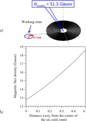
Note that the DNA manipulation zone, a gold-patterned surface, is located at the center of the six coils within a radius of 500µm. Figure 4(b) shows the simulated magnetic flux density inside the working zone. It shows that the field gradient is a constant value 1.33 T/m. Thus, one can obtain a nearly uniform, pico-Nt magnetic force using these microcoils.
(a)
(b)
Figure 4: The magnetic field generated by one of the microcoils was numerically calculated using FEA software. (a) The simulation model of the microcoil. The DNA manipulation zone was located at the center of the six coils within a radius of 0.5 mm. (b) The magnetic flux density inside the DNA manipulation zone as a function of the distance away from the center of the six coils. Note that the applied current is 250 mA.
Figure 5: The measured flux density versus the applied currents at the center of the microcoil. The magnetic field was measured using a Tesla meter.
PI coating and bonding pads opening PR molding for conductor pattern
Copper coil electroplating
PI patterning and via electroplating
Upper copper coil electroplating
Localized gold lift-off
Flow cell assembly
Coverslip Double-side
sticky tape Fluidic channel
0 0.5 mm
Bcenter= 51.3 Gauss
Working zone
0 0.1 0.2 0.3 0.4 0.5
Distance away from the center of the six coils (mm) 12
13 14 15 16 17 18 19
Magnetic flux density (Gauss)
0 0.1 0.2 0.3 0.4 0.5
Current (A) 0
20 40 60 80 100 120
Flux density (Guass)
To verify the simulation data, the magnetic field was measured using a Tesla meter (TM-401, KANETEC) and the plot of the flux density versus the applied currents is shown in Fig. 5. When applying a current of 0.25 A on the coil, the flux density at the center of a coil is about 50 Gauss, which is very consistent with the simulated data.
Using a simple calculation, one can get a field gradient about 1 T/m at the center of hexagonally-aligned microcoils, which is again highly consistent with the numerical data. According to the simulation and experimental results, our designed magnetic tweezers could generate a pico-Nt force to manipulate a single DNA.
2.3 DNA Sample Preparation
For achieving specific attachment of λ-DNA (NEB Inc.) onto the magnetic beads and the gold surfaces, molecular self assembly techniques were used to build a highly efficient and specific DNA construction.
First, a complementary primer containing a biotin molecule was custom-synthesized. Using DNA hybridization and ligation process, one end of DNA could be biotinylated. Subsequently, the biotinylated λ- DNA was purified to remove excess olignucleotide.
Secondly, another extremity of the biotinylated λ- DNA was filled with the desired thiol group by a standard reaction using Klenow fragment of DNA polymerases and S4-dTTP (Trilink Biotechnologies Inc.), dATP, and dGTP (NEB Inc.) [8]. To remove excess deoxynucleoside triphosphates and protein, λ-DNA was again purified. Since this technique could be incorporated with five thiol groups at the end of the λ- DNA, a highly efficient binding between the end of thiol-modified λ-DNA and Au would be achieved [8].
Consequently, one end of the λ-DNA was labeled with biotin and bonded to a 2.8-µm streptavidin-coated magnetic bead (M280, Dynal). Another extremity, which was incorporated with S4-dTTP using the Klenow fragment, would covalently bind on the Au surface.
Finally, the tethered-bead and thiol-modified λ-DNA was transported into the fluidic channel and was immobilized on DNA manipulation platform.
2.4. Fluorescence Microscopy
In order to visualize a single DNA molecule, the λ- DNA was stained with YOYO-1 dyes (Molecular Probes Inc., USA). The base pair to dye molecule ratio was kept at 5:1 for DNA solutions to have a better signal-to-noise ratio. An oxygen scavenging system was mixed with the DNA to reduce photo-bleaching and photo-scission effects. Typically, a single molecule could be observed for a period of 10 min without breaching.
The fabricated device was mounted on top of an inverted microscopy (IX-70, Olympus, Japan) for DNA visualization, which was equipped with a fluorescence source (75 W Xenon lamps, UXL-S75XE, Ushio Inc., Japan) and a standard YOYO-1 filter set. The fluorescence image of the single DNA molecule was acquired by an oil-immersion objective lens (Plan Apo, NA = 1.35, Olympus, Japan), as well as a cooled CCD
(CCD-300T-RC, DAGE-MTI, USA), an image integrator (Investigator, DAGE-MTI, USA) and a video recorder (NV-F86TN, Panasonic, Taiwan). At last, a frame grabber (Bandit-II CV, Coreco Imaging, USA) was used to digitize the recorded images.
3. RESULTS AND DISCUSSIONS
Figure 6 shows successful stretching of a single DNA molecule linked to a localized gold surface using the magnetic force generated by applying currents on the microcoils. The DNA was stretched to 12.28 µm as the applied current increased to 250 mA.
Fig. 6. The stretching of a single DNA molecule linked to a localized gold surface using the magnetic force generated by using the developed platform.
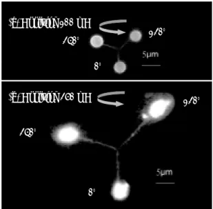
Fig. 7. Three time series of counter-clockwise rotation of a single DNA molecule by applying a circular permutation of the currents to hexagonally-aligned microcoils. (a) 100 mA, and (b) 250 mA.
Figure 7 shows three time series of rotation of a λ- DNA in the magnetic field. Counter-clockwise rotation of a single DNA molecule linked to the gold surface could be achieved by applying a circular permutation of the currents to the hexagonally-aligned microcoils. While applying a smaller current (100 mA) on the three microcoils, the revolving radius of the tethered-bead DNA is about 5 µm as shown in Fig. 7(a). A bigger current of 250 mA could generate bigger magnetic forces to stretch and rotate the tethered-bead DNA with a longer radius as shown in Fig. 7(b).
0°
240° 120°
(a) Applying 100 mA
240°
120°
0°
(b) Applying 250 mA
Multiple DNA molecules were also found to attach onto a single bead and immobilized separately onto the gold surface. Figure 8 shows the stretching of two DNA molecules. The phenomenon could be used to investigate the interaction of two DNA molecules and the corresponding physical properties of twisted DNA strains.
Fig. 8. The stretching of two DNA molecules. Two-DNA molecules were attached to a single bead and immobilized onto the gold surface.
The magnetic forces acting on the bead were also measured. The free-body diagram of the tethered-DNA bead (Fig. 1(B)) shows that the bead is in equilibrium under the action of DNA elastic force, gravity force, and magnetic force. These experimental data were then confirmed using the Worm-Like Chain (WLC) model.
The mechanical response of a single DNA molecule to the applied force lies in the entropic regime, in which the stretching force is less than 6 pN [3]. Figure 9 shows the relation between extension of a single DNA molecule and stretching force. Experimental data are in agreement with the result from the WLC model. Using Hook’s law, the DNA spring constant is measured to be about 10-8∼ 10-7 Nt/m
Fig. 9. Force-extension curve for a single λ-DNA molecule
4. CONCLUSIONS
We have demonstrated a new DNA manipulation platform capable of stretching and rotation of a single DNA molecule using MEMS technologies. For specific attachment to magnetic beads and the gold surface, a highly efficient and strong affinity binding systems of
DNA two sticky ends were successfully developed. The DNA manipulation platform has great potential to observe the physiological behavior of a single DNA molecule and investigate the physical properties with a real-time fashion. Experimental data were in reasonable agreement with the theoretical values, and the DNA spring constant was measured to be about 10-8∼10-7 Nt/m.
This new tool has several advantages over its large- scale counterparts including higher spatial resolution, MEMS compatibility, cost-effectiveness, excellent operation control, and flexibility to integrate with other MEMS devices. The outcomes of this study could provide a powerful tool for the study of the bio-physical properties of bio-molecules, biopolymers, and cells, which will make substantial impacts on development of nano-biotechnology.
ACKNOWLEDGEMENTS
This work is supported by National Science Council in Taiwan under a grant number NSC-92-2212-E-006- 068.
REFERENCES
[1] T. T. Perkins, S. R. Quake, D. E. Smith, S. Chu,
“Direct observation of tube-like motion of a single polymer chain,” Science, Vol. 264, pp. 822-826, 1994.
[2] T. Strick, J. F. Allemand, D. Bensimon, A.
Bensimon, V. Croquette, “The elasticity of a single supercoiled DNA molecule,” Science, Vol. 271, pp.
1835-1837, 1996.
[3] G. V. Shivashankar and A. Libchaber, “Single DNA molecule grafting and manipulation using a combined atomic force microscope and an optical tweezer,” Appl. Phys. Lett., Vol. 71, pp. 3727- 3729, 1997.
[4] B. Essevaz-Roulet, U. Bockelmann, F. Heslot,
“Mechanical separation of the complementary strands of DNA,” Proc. Natl. Acad. Sci. USA., Vol.
94, pp. 11935-11940, 1997.
[5] C. Haber, D. Wirtz, “Magnetic tweezers for DNA micromanipulation,” Rev. Sci. Instrum., Vol. 71, pp. 4561-4570, 2000.
[6] C. Gosse, V. Croquette, “Magnetic Tweezers:
Micromanipulation and Force Measurement at the Molecular Level,” Biophys. J., Vol. 82, pp. 3313- 3329, 2002.
[7] Romano, G., Sacconi, L., Capitanio, M., Pavone, F.S., “ Force and torque measurements using magnetic micro beads for single molecule biophysics”, Opt. Commun. 215, 323-331, 2003.
[8] Zhang Y, Austin R H, Kraeft J, Cox E C and Ong N P 2002 Insulating behavior of λ-DNA on the micro scale Phys. Rev. Lett. 89 198102 DNA extension length (µm)
0 2 4 6 8 10 12 14
DNA elastic force (pN)
0.00 0.05 0.10 0.15 0.20 0.25 0.30
Relative extension
0.0 0.1 0.2 0.3 0.4 0.5 0.6 0.7 WLC model
Experimental data
New Fabrication of Monolithic Probes with Integrated Electrical Heaters for Nano-thermomechanical Writing
Shang-Jen Chang, Chi-Han Chiou, Gwo-Bin Lee, Huei-Huang Lee Department of Engineering Science
National Cheng Kung University, Tainan, Taiwan, R.O.C. 701
Author for Correspondence: Gwo-Bin Lee E-mail: [email protected]
ABSTRACT
This study reports a new fabrication process for a micromachined probe. The micro probe comprised a micro- cantilever, a nano-tip and a supporting substrate, which are monolithically made of single-crystalline silicon. The fabrication process started with a bi-layer silicon wafer made of a 20-µm-thick epitaxial Si layer with heavily- boron doping and a 400-µm-thick bulk Si substrate. The tip with a radius of curvature of 50 nm was formed by anisotropic etching followed by oxidation sharpening process. Then a cantilever beam was released by back-side etching of an etch-stop Si layer. The spring constants of the cantilevers ranging from 0.03 to 0.4 N/m have been determined by the FEA (finite element analysis), the static measurements using an AFM system and the dynamic measurement using a LDV (laser Doppler vibrometer) system. Most importantly, the Young’s modulus of the thin-film materials could be confirmed with these methods.
The developed probe was also integrated with a Pt-heater to apply to thermal writing on PMMA substrates. Preliminary experiments for the thermal writing have been conducted by localized heating of the tip. The cantilever tip was heated to above 120 ℃to create an 800-nm width line. In conclusion, the feasibility for nano-applications including data storage and nanolithography using the developed probe with a heater has been successfully demonstrated.
The development of the probes could be of crucial needs for nano-machining.
Keywords: AFM probe, Epitaxial wafer, Spring constant, Resonant frequency, Micro-heater, Thermal writing
1. INTRODUCTION
Microfabricated probes have been widely used for many applications including the atomic force microscope (AFM) [1-2], lithography [3], and data storage [4-6]. Many existing processes have been reported for probes using MEMS (Micro-electro-mechanical-systems) technologies.
For example, a single-crystal silicon was usually preferred for constructing a cantilever beam due to its low intrinsic stress and controllable material quality [1].
In fact, SOI (silicon on insulator) wafers were popularly employed as the starting materials to fabricate thin cantilever beams [5-8]. However, the process to form the cantilever beams was time-controlled etching, resulting in a variation of beam thickness. Moreover, when using SOI wafers as the starting materials, a silicon dioxide layer served as an intermediate layer between the cantilever beam and the silicon substrate, which could introduce a mismatch between the silicon and the silicon dioxide material. Recently, Liu et al. employed a three-layer silicon wafer that consisted of an epitaxial layer, a heavily doped layer, and a silicon substrate to fabricate a monolithic silicon probe [2]. Even though SOI wafers or three-layer epitaxial wafers are suitable for fabricating a single-crystal silicon beam with a nano-scale tip, they are very expensive and using them results in raising the production cost of the probes. Thus, the major drawbacks of the previous methods still overshadow their wide applications.
It is important to precisely determine the spring constant of the cantilever. Usually, the spring constant of the probe can be calculated by using the cantilever formula based on its dimensions and bulk material properties [9].
This method generated wider variations due to difficulties in controlling the cantilever thickness in the back-side etching process. Also, the Young’s modulus of thin film may not be identical to those of the bulk materials [10].
Alternatively, to determine the spring constant, the static measurement of the cantilever could be realized by using an AFM system based on the force-distance curve [7, 11].
Although it was not necessary to know the dimensions and the material properties of the cantilever, it may generate larger errors on the determination of the spring constants [11]. On the other hand, the dynamic measurement of the cantilever was commonly used to determine the spring constant [7, 12].
In this study, we report a new, simple, reliable, and low cost method to fabricate micro probes by using bi-layer silicon wafers consisting of a layer of epitaxial-growth single crystal silicon with heavy boron doping. The fabrication process to produce a monolithic probe comprising a nano-tip, a micro-cantilever, and a supporting substrate is based on thermal oxidation sharpening, etching- stop, and anisotropic etching techniques. The spring
constant and natural frequency of the fabricated probes were first determined by finite element analysis (FEA) and further confirmed by using an AFM system and the laser Doppler vibrometer (LDV) system, respectively. With these methods, one can determine the spring constants in the range of 0.03 ~ 0.4 N/m with high accuracy, and most importantly, can confirm the validity of the Young’s modulus of the material.
In addition, the major advantage of MEMS technologies is that a probe can be easily integrated with a heater on thermal writing applications. Originally, writing was performed by heating the tip with a laser beam [4].
However, the lasers were bulky and required precise alignment. Recently, some simplification has been reported by employing a probe integrated with an electrical heater instead of the focused laser beam. Previously, most heaters were realized by adapting SOI wafers [5-6]. Alternatively, we have fabricated a probe with an integrated Pt-heater using a bi-layer wafer and further applied the developed probe by localized heating the tip for thermo-machining on the PMMA (polymethyl methacrylate) substrate.
2. DESIGN AND FABRICATION 2.1 Design
Considering the spring constant (kf ) of a fixed-free cantilever with rectangular cross-section, the following equation is under the small displacement assumption [9].
3
43 f
k Ewt
= l (1) Where w is the width, t is the thickness, l is the length, and E denotes the Young’s modulus of the probe material.
In our case, since the cantilever beam is made of an epitaxial-layer with heavily doped boron, the thickness of the cantilever beam will depend on the etch-stop layer, and the Young’s modulus of single crystal silicon with heavy boron doping is approximately 92 GPa, which was obtained by the preliminary experiment as previously described [10].
All design parameters for six micro-probes are listed in Table 1.
Table 1: All design parameters for the micro-probes.
Type Dimensions l×w×t (µm)
Spring constant
(N/m) Resonant frequency (Hz)
A 2000 × 50 × 14 0.394 3613
B 2500 × 50 × 14 0.202 2312
C 3000 × 50 × 14 0.117 1601
D 3500 × 50 × 14 0.074 1180
E 4000 × 50 × 14 0.049 903
F 4500 × 50 × 14 0.035 714
The resonant frequency ( fr ) for a singly clamped cantilever could be calculated as follows [9].
1 1.03 1.03
2
f f f
r
e b
k k k
f = π m ≈ π m ≈ π ρlwt (2) Where ρ is the density of the silicon beam, mb is the beam mass and me ≈0.24mb is the effective mass of the beam. Thus, for given dimensions of the cantilever, the spring constant can be determined by measuring the resonant frequency. Table 1 also lists the designed resonant frequency corresponding to the spring constants.
Nevertheless, the spring constant can still be difficult to determine from these two equations because the process and thin-film materials used to fabricate the cantilevers may create the uncertainties in dimensions and Young’s modulus. Therefore, in this work, a combination method of theory and measured mechanical properties associated with the cantilever beam will be exploited in the determination of the spring constant, resonant frequency, and Young’s modulus.
Thermal-mechanical writing can be achieved by applying a local force through the probe integrated with an electrical heater in contact with a polymer substrate, and simultaneously softening the polymer substrate by localized heating. Hence, the cantilever tip must be heated above the glass transition temperature of the polymer (which is approximately 120 ℃ for PMMA) to initiate the softening.
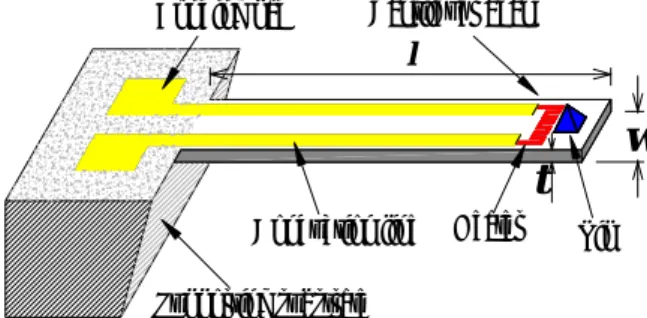
In this work, the electrical heater was designed for heating a tip by thermal conduction. The heater consists of a Pt heating region with a high resistivity (10.6 × 10⁻⁶ Ω-cm) and an Au conductor line with a low resistivity (2.2 × 10⁻⁶ Ω-cm). Figure 1 shows a schematic representation of the probe integrated with a heater and a heater layout.
Figure 1: A schematic diagram of a probe integrated with a heater.
2.2 Fabrication
Simplified fabrication process is shown in Fig. 2. The process started with a bi-layer silicon wafer. The substrate is a 400-µm thick, {100} oriented, and 4-inch diameter silicon wafer, which forms the supporting element. The front surface of the wafer is made of an epitaxial-growth single crystal silicon layer, which is heavily boron doped by ion-implantation (1×10¹⁹ ~ 1×1020 cm-3) used for etching stop. The thickness of the epitaxial layer is typically 20 µm.
l
Bonding pad Cantilever beam
Heater Conduction line
Supporting substrate
Tip
w t
Figure 2: The simplified fabrication process for the probe comprising a cantilever beam, a nano-tip, and a heater.
First, 1 µm silicon dioxide was grown on top of the epitaxial layer by thermal oxidation and patterned by photolithography and a 6:1 BOE (buffered oxide etchant, J.
D. Baker, USA) wet etching to define the tip mask. Next, the epitaxial-growth single crystal silicon layer was etched using TMAH (tetra methyl ammonium hydroxide, 25 % in water, J. D. Baker, USA) via the oxide tip mask to form the tip. In this process, to achieve a sharp tip, an oxidation sharpening process was employed to allow us for rough controlling of etching parameters such as time, and temperature. After two sharpening cycles, a 5-µm thick sharp tip with a radius of curvature of 50 nm could be formed as shown in Fig. 3(a).
(a) (b)
Figure 3: SEM images of the fabricated probes consisting of a tip, a cantilever, and a supporting substrate. (a) The tip after two sharpening cycles with 0.5 µm growth. The radius of curvature of the tip is estimated to be 50 nm. (b) The probe array. Note that the fabrication process did not include metallization.
Upon completion of the tip fabrication, the wafer was again thermally oxidized and patterned. This oxide layer (500 A thick) served as a protection for the tip and as an insulation layer between the metals and the heavily doped silicon. Subsequently, for fabricating a heater on the probe, platinum was used for a resistor while gold was used to as a conductor. A layer of Pt/Cr (2000 A。 /200 A。) was deposited using electro-beam evaporation and patterned using standard lift-off techniques to form a heating element.
Again, a layer of Au/Cr (2000 A。 /200 A。) was deposited using electro-beam evaporation and patterned using wet etching to form a conduction line.
Following the completion of the heater, a 10-µm thick photoresist layer (AZ 4620, Clariant Corp., Switzerland), which was covered on the tip apex, served as a protective layer during reactive ion etching (RIE) process. The cantilever beam with the 14-µm thick vertical-sidewall was well-defined by adapting RIE using SF6, O2, and Ar.
Afterwards, an etch window on the backside was opened in the oxide layer (500 A。 thick) using BOE solution. To protect the structures on the front side from damage during the backside etching process, a protective layer (ProTEK Primer/B1-18, Brewer Science, Inc. USA), which was multi-coated on top of the wafer, was used to withstand at least 10 hours exposure to TMAH solution. Subsequently, the unwanted silicon substrate was removed using TMAH at 90 ℃. The etching process would be stopped on the layer with heavily boron doping, namely the etching-stop technique, resulting in a release of a freestanding cantilever.
Finally, the protective layer and the insulation layer could be easily removed with acetone and BOE, respectively, and finished a probe integrated with a micro-heater. The photograph of the completed probe is shown in Fig. 4. Note that if the heater is not necessary and the process can be simplified to fabricate an AFM probe. The scanning electron micrograph of the freestanding micro-probes without heaters is shown in Fig. 3(b).
Figure 4: The picture depicting the fabricated probe integrated with a micro-heater.
3. RESULTS AND DISCUSSIONS 3.1 Static Characterization
In order to quantify the performance of the fabricated probes, the static and dynamic methods for determining the
200 µm Tip
Cantilever
Conduction line Heater
200 µm 3 µm
Starting with bi-layer Si wafer
Cantilever release using TMAH Thermal oxidation and
tip mask patterning
Cantilever patterning using RIE
Tip etching
Tip sharpening and insulation
Pt-heater deposition and patterning
Au-conductor pattering
Front-side protection using ProTEK Primer/B1-20
Removal of protective and oxide layers Bulk silicon: 400 μm
Epitaxial layer: 20 μm
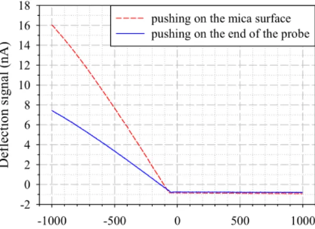
mechanical properties of the probes were performed. First, the measurement of static defection of the probes could be realized by using the AFM system (Solver P7LS SPM, NT- MDT Corp., Russia) based on the force-distance curve. A schematic diagram of the measurement system is depicted in Fig. 5. First, the standard AFM probe was driven vertically against the mica substrate as shown in Fig. 5(a).
It could obtain a force curve which depicted the defection of the standard AFM probe as a function of the piezoelectric scanner displacement (dashed line in Fig. 6).
The next step was to land the free end of the fabricated probe on the end of the standard AFM probe as shown in Fig. 5(b). Owing to mutual bending of two cantilevers during the approach, the slope of the force curve (solid line in Fig. 6) was smaller than the case of landing on the mica surface.
Figure 5: A schematic diagram of the static method for measuring the spring constant by an AFM system. The standard AFM probe is vertically landing (a) the mica surface, and (b) the free end of the fabricated probe. The slopes of the force curves in these two cases can be obtained by measuring deflections of the standard AFM probe.
As the forces acting on two cantilevers are equal, the following equation could be obtained.
k zs∆ = ∆s k zf f (3) Where ks is the spring constant of the standard AFM probe, kf is the spring constant of the fabricated probe,
zs
∆ and ∆zf are the defections of the standard AFM probe and the fabricated probe, respectively. Since these two probes were constrained by hard stages, the piezoelectric scanner displacement ∆zPZT should be equal to ∆ + ∆zs zf. Hence,
k zs∆ =s kf(∆zPZT − ∆zs) (4) The quantitative value of ∆zPZT can be determined from the slope of the force curve (Slopemica, dashed line in Fig. 6) when pushing on the mica surface, and the quantitative value of ∆zs can be determined from the slope of the force curve (Slopefree, solid line in Fig. 6) when
pushing on the freestanding end of the fabricated probe.
Hence, Eq. (4) can be presented as follows.
1
( ) 1
free
f s s
mica free mica free
Slope
k k k
Slope Slope Slope Slope
= =
− − (5)
Given a known ks, the spring constant of the fabricated probe can be determined by the slopes of the force curves.
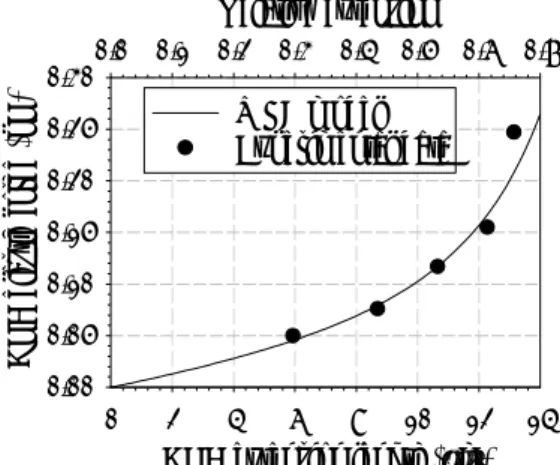
In order to perform accurate measurements in the range of 0.03 to 0.4 N/m, a standard AFM probe with the spring constant of 0.075 N/m was employed. Figure 6 shows an example of the force curve for Type-D cantilevers. In the linear region, the slope when pushing on the mica surface was 2.1 times steeper than the slope in the case of pushing on the free end of Type D. Using Eq. (5), the spring constant of Type-D cantilevers was estimated to be 0.068 N/m, which is highly consistent with the designed value of 0.074 N/m obtained by Eq. (1). The experimental results for all cases are summarized in Fig. 7. The results indicate that appreciable discrepancy exists between the measured and theoretical values. This is due to the facts that uncertainties of E and t used in Eq. (1) depending on how accurately to control the fabrication parameters. With this method, the spring constants can be directly measured without any knowledge of dimensions and material properties. However, the validity still requires to further be confirmed with dynamic measurements.
Figure 6: The force curve showing the deflection of a standard AFM probe as a function of the piezoelectric scanner displacement (Type D). In the linear region, the slope when pushing on the mica surface (dashed line) is 2.1 times steeper compared to the case of pushing on the free end of probe Type D (solid line).
3.2 Dynamic Characterization
In order to calculate the natural frequency of the fabricated probe, a FEA software called ANASYS 6.0 was used. A mesh generated by Solid 95 elements was created to fit the shape of the probe with a tip. All dimensions of the fabricated probes were measured by a scanning electro microscope. For example, the l, w, and t for Type-D
Mica substrate Standard AFM probe
Fabricated probe PSPD
Laser diode
Piezoelectric scanner
Mica substrate
(a) (b)
ZPZT
∆
Zs
∆
PSPD Laser diode
Zf
∆
Piezoelectric scanner
Piezoelectric scanner displacement (nm)
-1000 -500 0 500 1000
Deflection signal (nA)
-2 0 2 4 6 8 10 12 14 16
18 pushing on the mica surface
pushing on the end of the probe
cantilevers were 3500 µm, 50 µm, and 14 µm, respectively.
The FEA result of Type-D cantilevers shows the resonance frequency of 1163 Hz. The simulation results were further compared with experimental data obtained by the LDV system (Microscope Scanning Vibrometer, MSV 300, Polytec, Inc., Germany) based on the Doppler shifts in the reflected light.
Figure 7: The plot showing comparison of spring constants determined by the theoretical formula (solid line), FEA (circle), the slopes of the force curve (square), and resonant frequency method (triangle). It indicates the error between designed and measured values is within 14 %. The errors are due primarily to uncertainties in the Young’s modulus and thickness caused by fabrication process.
In one of the cases (Type D), the frequency spectrum was shown in Fig. 8. The peak in Fig. 8 represented the natural frequency f , which was found to be 1159 Hz. r Substituting for fr, l, w, and t into Eq. (2), one can obtain the spring constant to be 0.071 N/m, which is consistent with the static measured value of 0.068 N/m. Figure 7 shows a comparison of the results obtained by the theoretical formula, FEA, AFM measurements, and LDV measurements. In a comparison with the simulation and experimental data, it indicates the error is within 14 %.
However, experimental data from the AFM and LDV are highly consistent. Thus, the calibration with these methods provides high accuracy in the determination of the spring constant.
As expected, the discrepancy between the designed values and the measured values is due primarily to uncertainties of fabrication process. Moreover, Eq. (1) and (2) did not take into account of the tip mass, resulting in the errors of the calculating spring constants. If the measured spring constant and thickness substitute into Eq. (1), the Young’s modulus can be solved to be about 90 GPa, which is highly consistent with the referred value. According to the experimental and theoretical results, the spring constants of the fabricated probes have been precisely calibrated in the range from 0.4 to 0.03 N/m, which are useful for most SPM applications. Most importantly, the
Young’s modulus of the thin-film materials can be confirmed with high accuracy.
Figure 8: The frequency spectrum of the fabricated Type-D probe. The peak at 1159 Hz represents the resonance frequency.
3.3 Thermal writing
The developed probe with an integrated micro-heater was further applied to thermal writing on PMMA substrates.
First, it is necessary to determine the thermal characteristics of the micro-heater. The Pt-heater treated with a sintering process could reach a reliable TCR of approximately 0.26
%/℃. In our case, the heaters were located close to the tip, and a tip was made of the heavily doped-Si material with highly thermal conductivity. Consequently, the localized heat generated by applying a pulsed current on the heater was quickly transferred to the tip apex. Thus, it allowed for a less heating time and cooling time for writing on PMMA due to the small thermal capacity.
(a)
(b)
Figure 9: An atomic force micrograph of the thermal wiring by heating the tip in contact with the PMMA substrate. (a) The AFM image showing a pit of 4 µm × 4 µm could be formed. The pit size corresponds to the base of the tip. (b) 3-D rendering of an 800-nm width line written with workpiece movements. It demonstrates that the feasibility for nanolithography using the developed probe integrated with a micro-heater.
4 µm
800 nm
Cantilevr length (µm)
1500 2000 2500 3000 3500 4000 4500 5000
Spring constant (N/m)
0.00 0.05 0.10 0.15 0.20 0.25 0.30 0.35
0.40 Theoretical data by Eq. (1)
Simulation data by ANSYS Static measurement by AFM Dynamicmeasurement by LDV
Frequency (Hz)
0 500 1000 1500 2000 2500 3000 3500 4000
Amplitude (nm)
-1 0 1 2 3 4 5 6
Subsequently, the developed probe was mounted on the AFM scanner, and the PMMA substrate was placed on an X-Y-Z stage such that one can manipulate 3-D movements of the workpiece. When applying a voltage of 3.5 V on the heater, the cantilever tip was heated to above the glass transition temperature of PMMA (120 ℃ ) to create a micro-pit. Basic operation functions of the probe with integrated heaters have been demonstrated as shown by the AFM image in Fig. 9. In Fig. 9(a), the indentation was conducted by heating the tip in contact with the PMMA substrate. Note that the pit of about 4 µm reflected the shape of the tip. Figure 9(b) shows an AFM image of the 800-nm width line written with the heated tip while dragging the probe along a straight line. It is important to verify that the pattern in nano-meter level can be realized with relative movements between the tip and the workpiece.
With sharper tips that allowing for smaller pits, it may be possible to generate narrower patterns. According to the experimental results, the PMMA substrate can be successfully written by the heated tip located on a probe.
4. CONCLUSIONS
We have successfully developed a new and low-cost method to fabricate monolithic silicon probes integrated with a micro-heater. Instead of using the SOI or three-layer epitaxial Si wafers as previously reported, the process employed a bi-layer Si wafer consisting of an epitaxial layer with heavily-boron doping and a bulk Si substrate.
With the fabricated probes, the spring constants and resonance frequency ranging from 0.03 to 0.4 N/m and 0.7 to 4 kHz, respectively, have been precisely determined by the FEA, an AFM system, and a LDV system.
In addition, we have also applied the developed probe with an integrated Pt-heater to thermal writing on PMMA substrates. Preliminary experiments for the thermal writing have been successfully conducted by localized heating the tip. The cantilever tip was heated to above 120 ℃ to create a 4-μm pit and an 800-nm width line. The feasibility for future nano-applications including data storage and nanolithography using the developed probe with the integrated heater has been successfully demonstrated. In conclusion, these fabricated probes have advantages over commercially-available probes, including (1) excellent mechanical strength and flexibility, (2) cost-effectiveness, (3) easy integration, and (4) versatile applications. Most importantly, the probes can be constructed by simple MEMS fabrication techniques such that it has great versatility and could be used for a wide range of nano- technology applications.
5. ACKNOWLEDGENENTS
The current authors gratefully acknowledge the financial support provided to this study by the National Science Council of Taiwan under Grant No. NSC-92-2212- E-006-068 and the support provided by the MOE Program
for Promoting Academic Excellence of Universities under Grant No. EX-91-E-FA09-5-4. Authors also thank Center for Micro-Nano Technology, National Cheng Kung University for access of major fabrication equipment.
6. REFERENCES
[1] T. R. Albrecht, S. Akamine, T. E. Carver, and C. F.
Quate, “Microfabrication of Cantilever Styli for the Atomic Force Microscope,” J. Vac. Sci. Technol. A, Vol. 8, pp. 3386-3396, 1990.
[2] C. Liu, and R. Gamble, “Mass-producible Monolithic Silicon Probes for Scanning Probe Microscopes,”
Sensors and Actuators A, Vol. 71, pp. 233-237, 1998.
[3] S. Lee, J. Kim, W. S. Shin, H. J. Lee, S. Koo, and H.
Lee, “Fabrication of Nanostructures Using Scanning Probe Microscope Lithography,” Materials Science and Engineering C, Vol. 24, pp. 3-9, 2004.
[4] H. J. Mamin, L. S. Fan, S. Hoen, and D. Rugar, “Tip- Based Data Storage Using Micromechanical Cantilevers,” Sensors and Actuators A, Vol. 48, pp.
215-219, 1995.
[5] D. W. Lee, T. Ono, and M. Esashi, “Electrical and Thermal Recording Techniques Using a Heater Integrated Microprobe,” J. Micromech. Microeng., Vol. 12, pp. 841-848, 2002.
[6] U. Drechsler, N. Burer, M. Despont, U. Durig, B.
Gotsmann, F. Robin, and P. Vettiger, “Cantilevers with Nano-heaters for Thermomechanical Storage Application,” Microelectron. Eeng., Vol. 67-68, pp.
397-404, 2003.
[7] D. Saya, K. Fukushima, H. Toshiyoshi, G.
Hashiguchi, H. Fujita, and H. Kawakatsu,
“Fabrication of Single-crystal Si Cantilever Array,”
Sensors and Actuators A, Vol. 95, pp. 281-287, 2002.
[8] A. Gupta, J. P. Denton, H. McNally, and R. Bashir,
“Novel Fabrication Method for Surface Micromachined Thin Single-crystal Silicon Cantilever Beams,” IEEE J. Microelectromech. Syst., Vol. 12, pp. 185-191, 2003.
[9] W. F. Stokey, Shock and Vibration Handbook, McGraw-Hill, New York, pp 7.1-7.44, 1989.
[10] H. C. Tsai, and W. L. Fang, “Determining the Poisson’s Ratio of Thin Film Materials Using Resonant Method,” Sensors and Actuators A, Vol.
103, pp. 377-383, 2003.
[11] C. T. Gibson, G. S. Watson, and S. Myhra,
“Determination of the Spring Constants of Probes for Force Microscopy/Spectroscopy,” Nanotechnology, Vol. 7, pp. 259-262, 1996.
[12] J. Yang, T. Ono, and M. Esashi, “Mechanical Behavior of Ultrathin Microcantilever,” Sensors and Actuators A, Vol. 82, pp. 102-107, 2000.
成效與貢獻
一、 論文發表
A. Conference Paper
1. Chi-Han Chiou, Gwo-Bin Lee, "Magnetic Tweezers for Manipulation of Single DNA Molecule", The 7th Nano Engineering and Micro System Technology Workshop, Taipei, Taiwan, November 20-21, 2003.
2. Shang-Ren Chang, Chi-Han Chiou, Huei-Huang Lee, Gwo-Bin Lee "Design and Fabrication of a Micro/Nano Probe and Its Characterization by AFM", The 27th Conference on Theoretical and Applied Mechanics, Tainan, Taiwan, December 12-13, 2003.
3. Chi-Han Chiou, Zhao-Fu Tseng, Gwo-Bin Lee, "A Novel Magnetic Tweezers for Manipulation of Single DNA Molecule", IEEE MEMS 2004, Maastricht, The Netherlands, January 25-29, 2004.
4. Chi-Han Chiou, Gwo-Bin Lee, "Stretching and Rotation of a Single DNA Molecule Using a Micromachine-based Magnetic Manipulator", The 11th Symposium on Nano Device Technology (SNDT 2004), Hsinchu, Taiwan, May 11-13, 2004.
5. Chi-Han Chiou, Gwo-Bin Lee, " Single DNA Molecule Manipulation Using a Micro- Magnetic Platform ", Taiwan International Conference on Nano Science and Technology (TICON 2004), Hsinchu, Taiwan, June 30-July 3, 2004.
B. Journal Paper (submitted)
1. Chi-Han Chiou, Gwo-Bin Lee, "A Micromachined DNA Manipulation Platform for the Stretching and Rotation of a Single DNA Molecule", submitted to the Journal of Micromechanics and Microengineering.
2. Shang-Jen Chang, Chi-Han Chiou, Gwo-Bin Lee, Huei-Huang Lee. "Design, Fabrication and Characterization of Micro Probes Integrated with Micro Heaters and Their Applications on Nano-machining", submitted to the Journal of Micromechanics and Microengineering.
C. 學位論文
1. 張尚任,『新型微探針之設計製作與測試及其整合微加熱器在奈米加工之應用』,碩 士論文,國立成功大學工程科學系,台南市,2004。
一、 成果自評
(1) 研究成果與預期完成工作項目之比較
(1) 預期:製作微型探針陣列,在探尖整合奈米級加熱器與溫度感測器。並在懸臂樑 上電鑄磁性合金,製作微型線圈。
研究成果:已完成
(2) 預期:完成 DNA 操縱平台相關元件之製作。將微線圈、微流道、力傳感器、
DNA 樣品與螢光偵測系統等 DNA 操縱元素整合在一起,完成 DNA 操縱平台之 組裝。
研究成果:已完成
(3) 預期:DNA 特定端固定技術(一端生物素修飾,一端以硫醇基修飾,或者兩端 以硫醇基修飾)
研究成果:已完成
(4) 預期:建立高解析度與高量測範圍之 DNA 操縱平台。
研究成果:已完成
(5) 預期:建立拉力與伸長量曲線、不同超盤繞度下之拉力與伸長量之關係曲線。
研究成果:已完成
(6) 預期:量測 DNA 之 I-V curve,比較文獻結果,確立 DNA 是否為絕緣體。
研究成果:未完成
(7) 預期:利用第一年建立的可視化系統建立線上 DNA 操縱之即時影像。
研究成果:已完成
(2) 結語
本計畫研究內容與原計畫內容相符合,且執行成果達到預期之目標。其研究成果已 發表在國內外學術論文上(可參考前述一、 論文發表)。
本計畫所發展之微磁嵌具有以下優點:(1)非破壞性(2)適當的作用力範圍(3)
易操控(4)力學量測性佳(5)製作便宜且 IC 製程相容。微磁嵌操縱平台將可推廣至生 物奈米有機線材操縱平台,應用於生命科學與奈米科技領域。