n
+-GaAs/p
+-InAlGaP/n
+-InAlGaP Camel-Gate High-Electron
Mobility Transistors
Yu-Shyan Lin,a,zDong-Hai Huang,bWei-Chou Hsu,bTzong-Bin Wang,b Rong-Tay Hsu,cand Yu-Huei Wuc
a
Department of Materials Science and Engineering, National Dong Hwa University, Hualien 974, Taiwan b
Institute of Microelectronics, Department of Electrical Engineering, National Cheng-Kung University, Tainan, Taiwan
c
Land Mark Optoelectronics Corporation, Tainan, Taiwan
This investigation proposes InAlGaP/InGaAs camel-gate high-electron mobility transistors with inverted␦-doping layers 共CAM-HEMTs兲. CAM-HEMTs with various gate metals, including Au, Pt/Au, Ti/Au, and Ni/Au, are investigated. The CAM-HEMT with the Ni/Au gate metal exhibits the benefits of a large gate voltage swing共3.6 V兲, a high two-terminal gate-source breakdown voltage共⬎20 V兲, no bell-shaped gate current and temperature-insensitive threshold voltages. These characteristics are attributable to the inverted␦-doping layer, the large conduction-band discontinuity of the InAlGaP/InGaAs heterojunction, the large bandgap of InAlGaP and the high camel-gate barrier with the Ni/Au gate metal.
© 2005 The Electrochemical Society. 关DOI: 10.1149/1.2146717兴 All rights reserved. Manuscript submitted September 6, 2005; revised manuscript received October 21, 2005. Available electronically December 14, 2005.
Over the past several years, InGaP/InGaAs high-electron mobil-ity transistors 共HEMTs兲 have become one of the most important semiconductor devices used in microwave applications.1-3Several structures have been reported to improve the breakdown voltage of the heterostructure field-effect transistors共HFETs兲 without decreas-ing the current drivability, such as buried gate HFETs,4
metal-insulator-semiconductor FETs,5 and camel-gate FETs
共CAMFETs兲.6-10
In particular, the CAMFET provides several advan-tages, such as共i兲 the elimination of metallurgical difficulties associ-ated with metal-semiconductor contacts;共ii兲 the relative ease of ad-justment of the built-in voltage, and共iii兲 the potential for improving reliability at high temperatures. For high power applications, the device should have a high breakdown voltages and high current driving capability. The driving currents are directly related to the sheet charge density in the channel. An effective way to increase the sheet charge density is to use material systems with a large conduction-band discontinuity.10-15In principle, a larger conduction-band discontinuity corresponds to a larger sheet charge density, so the current driving capability is greater. The larger conduction-band discontinuity in HEMTs also reduces the output conductance and the real space transfer, improving the performance of the devices. Our previous studies demonstrated the use of alternative InAlAsSb/InP14,15 and InAlGaP/GaAs16 materials systems used in microwave devices. Recently, Liu et al. presented a series of GaAs/InGaP CAMFETs.8,10 However, no study has focused on GaAs/InAlGaP CAMFETs. Therefore, this work presents high-electron mobility transistors with the quaternary camel-gate and inverted ␦-doping layer 共CAM-HEMTs兲. The n+-GaAs/p+-InAlGaP/n+-InAlGaP camel gate is employed to
re-place the GaAs homojunction camel gate,6-8the GaAs/AlGaAs het-erojunction camel gate,6,7 the GaAs/InGaP heterojunction camel gate,9,10and the conventionally used Schottky gate.3,11,14The high-barrier gate can effectively prevent electron injection into the chan-nel. The good carrier confinement in the InAlGaP/InGaAs/InAlGaP heterostructure channel also reduces the substrate leakage current at elevated temperatures. The experimental data demonstrate the excel-lent output characteristics of the CAM-HEMT because of the design of the camel gate and the use of the InAlGaP/GaAs heterojunction.
Experimental
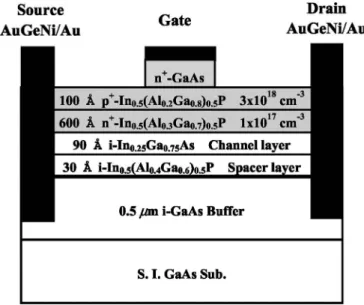
The CAM-HEMT was grown by metallorganic chemical-vapor deposition共MOCVD兲. The CAM-HEMT was grown on a Cr-doped semi-insulating GaAs substrate as the following layers −0.5m
un-doped GaAs buffer layer,␦-doping layer 共n+= 3.5⫻ 1012cm−2兲,
30 Å undoped In0.5共Al0.4Ga0.6兲0.5P spacer layer, 90 Å undoped
In0.25Ga0.75As channel layer, 600 Å n-In0.5共Al0.3Ga0.7兲0.5P 共n = 1
⫻ 1017cm−3兲, 100 Å p+-In
0.5共Al0.2Ga0.8兲0.5P 共p = 3 ⫻ 1018cm−3兲
and 200 Å n+-GaAs 共n = 4 ⫻ 1018cm−3兲. Figure 1 illustrates the cross section of the CAM-HEMT. The growth pressures of all of the layers were 100 Torr. The growth temperatures for InAlGaP and 共In兲GaAs were 700 and 650°C, respectively. Trimethylindium 共TMI兲, trimethylaluminum 共TMA兲, trimethylgallium 共TMG兲, arsine 共AsH3兲 and phosphine 共PH3兲 were used as sources of In, Al, Ga, As,
and P, respectively. Standard photolithography and lift-off methods were used to fabricate devices. The etchants for InAlGaP and GaAs were HCl and H3PO4:H2O2:H2O共1:1:30兲, respectively. The etching
rates of InAlGaP and GaAs were 50 and 15 Å/s, respectively. The etching solutions perform high-selectivity etching between InAlGaP and GaAs. AuGeNi/Au metal was used as the source and drain ohmic contacts. For comparison, four metals, including Au, Pt/Au, Ti/Au, and Ni/Au, were evaporated as the gate contact metals. The source, drain, and gate contact metals were deposited on the
z
E-mail: [email protected]
Figure 1. Schematic cross section of the InAlGaP/InGaAs CAM-HEMT. The n+-GaAs/p+-InAlGaP/n+-InAlGaP triple layers marked in gray represent the camel gate.
Electrochemical and Solid-State Letters, 9共2兲 G37-G39 共2006兲
1099-0062/2005/9共2兲/G37/3/$20.00 © The Electrochemical Society G37
n+-GaAs layer. After these contacts were formed, the CAM-HEMT
was dipped in the etchant to recess the partial n+-GaAs layer, which is not protected by the gate metal. The gate areas were 1.5 ⫻ 125 m. The source-drain spacing was 5 m. All the device characteristics of this proposed CAM-HEMT were measured using an HP-4156 semiconductor parameter analyzer.
Results and Discussion
Figure 2 depicts the current-voltage characteristics of the CAM-HEMT with an Ni/Au gate. The gate leakage current at VGS= 1 V is as small as 177A/mm. The threshold voltage 共Vth兲 of the
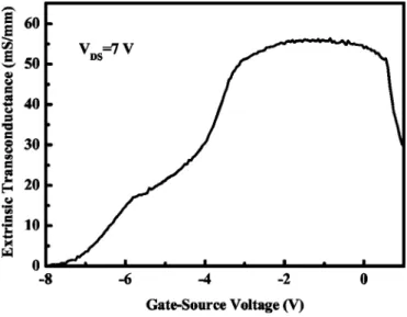
CAM-HEMT is −7.2 V because of the use of the inverted␦-doping layer. The gate turn-on voltage, measured at a forward gate current of 1 mA/mm, is 1 V. Figure 3 plots the extrinsic transconductance 共gm兲 vs VGSat a bias of VDS= 7 V. The gate voltage swing, defined
by a 10% drop in the maximum gm, is as large as 3.6 V, which can reduce the third-harmonic distortion and so serve as a linear ampli-fier. These characteristics are attributed to the inverted␦-doping and to the large⌬ECat the InAlGaP/InGaAs heterojunction. The design
of the inverted␦-doping increases the reversed operating voltage. Moreover, the large⌬EC of the InAlGaP/InGaAs/InAlGaP
hetero-junction leads to the strong carrier confinement. ⌬EC of the
In0.5共Al0.4Ga0.6兲0.5P/In0.25Ga0.75As is approximately 0.43 eV.17,18
This value exceeds those of Al0.3Ga0.7As/In0.2Ga0.8As 共0.407 eV兲 and In0.5Ga0.5P/In0.25Ga0.75As共0.34 eV兲. Figure 4 displays the
gate-source diode characteristics of the CAM-HEMT at 300 K. The breakdown voltage of the InAlGaP/GaAs CAM-HEMT, at which
Igs= 1 mA/mm, exceeds 20 V. This value is superior to those of the
␦-doping InGaP/InGaAs CAM-HEMT 共7.8 V兲9
and the
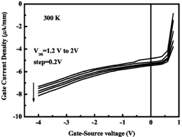
InGaP/InGaAs doped channel CAMFET 共16.5 V兲.10 The gate-dominated high-breakdown characteristics are attributed to the use of the high InAlGaP/GaAs camel-gate barrier, which reduces the thermionic-field emission. Table I summarizes the dc output charac-teristics of the HEMTs with different gate metals. The CAM-HEMT with Ni/Au gate has the largest two-terminal breakdown voltage and the smallest drain-source leakage current of the four CAM-HEMTs with different gate metals, because the barrier in the CAM-HEMT with the Ni/Au gate is highest. Figure 5 plots the gate current of the CAM-HEMT as a function of the gate-source voltage for VDSfrom 1.2 to 2 V. The gate current is as low as 8.2A/mm at Vgs= 4 V and Vds= 2 V. Notably, the gate current does not
ex-hibit the bell-shaped characteristics, which are commonly observed in the InGaAs-based HFETs. Additionally, the temperature depen-dence of the CAM-HEMT is also investigated. The Vth shift of CAM-pHEMT is very small in the temperature range 300–420 K. The K factor 共that is, Vth/T兲 of CAM-pHEMT at VDS= 7 V is
−1.6 mV/K. This result demonstrates the CAM-HEMT has the bet-ter thermal stability than the previously reported ␦-doped InGaP/GaAs FET.19
Conclusions
This study proposes a series of InAlGaP/InGaAs CAM-HEMTs with different gate metals. The barrier heights and dc characteristics for the CAM-HEMTs with various gate metals are examined. The
Table I. Comparison of the CAM-HEMTs with various gate met-als„Lg = 1.5 m….
Gate metal Pt/Au Au Ti/Au Ni/Au
q 共eV兲 0.816 0.842 0.852 0.867
BVgs共V兲 9.2 13.8 19 ⬎20
IDS,leakage共A/mm兲 at VDS= 0 V and VGS= 1 V
548 512 283 177
Figure 2. Current-voltage characteristics of the InAlGaP/InGaAs CAM-HEMT with the Ni/Au gate metal at 300 K.
Figure 3. Extrinsic transconductance of the CAM-HEMT with Ni/Au gate metal as a function of the gate voltage.
Figure 4. Two-terminal gate-source breakdown characteristics of the CAM-HEMT with the Ni/Au gate metal at 300 K.
G38 Electrochemical and Solid-State Letters, 9共2兲 G37-G39 共2006兲
G38
CAM-HEMT with Ni/Au exhibits a high breakdown voltage, large gate voltage swing, and good thermal stability. Accordingly, the CAM-HEMT developed herein is promising for high-power and high-temperature operations.
Acknowledgments
This work was supported by the National Science Council, Re-public of China, under contract no. NSC 93-2215-E-259-005.
Y.-S. Lin assisted in meeting the publication costs of this article.
References
1. P. Fay, K. Stevens, J. Elliot, and N. Pan, IEEE Electron Device Lett., 21, 141 共2000兲.
2. S. S. Kim and J. I. Song, IEEE Electron Device Lett., 22, 59共2001兲.
3. Y. S. Lin, W. C. Hsu, C. H. Wu, W. Lin, and R. T. Hsu, Appl. Phys. Lett., 75, 1616 共1999兲.
4. Y. Okamoto, K. Matsunaga, and M. Kuzuhara, Electron. Lett., 31, 2216共1995兲. 5. C. L. Chen, L. J. Mahoney, M. J. Manfra, F. W. Smith, D. H. Temme, and
A. R. Calawa, IEEE Electron Device Lett., 13, 335共1992兲.
6. R. E. Thorne, S. L. Su, W. Kopp, R. Fischer, T. J. Drummond, and H. Morkoç, J.
Appl. Phys., 53, 5951共1982兲.
7. H. Morkoç, Jpn. J. Appl. Phys., Part 2, 21, L233共1982兲.
8. J. H. Tsai, W. S. Lour, L. W. Laih, R. C. Liu, and W. C. Liu, Solid-State Electron.,
39, 343共1996兲.
9. J. H. Tsai, IEEE Electron Device Lett., 24, 1共2003兲.
10. P. H. Lai, H. M. Chuang, S. F. Tsai, C. I. Kao, H. R. Chen, C. Y. Chen, and W. C. Liu, Semicond. Sci. Technol., 19, 912共2004兲.
11. J. S. Su, W. C. Hsu, D. T. Lin, W. Lin, H. P. Shiao, Y. S. Lin, J. Z. Huang, and P. J. Chou, Electron. Lett., 32, 2095共1996兲.
12. J. M. Kuo, Y. J. Chan, and D. Pavlidis, Appl. Phys. Lett., 62, 1105共1993兲. 13. Y. C. Wang, J. M. Kuo, J. R. Lothian, F. Ren, H. S. Tsai, J. S. Weiner, J. Lin,
A. Tate, Y. K. Chen, and W. E. Mayo, Electron. Lett., 34, 594共1998兲. 14. Y. S. Lin, W. C. Hsu, C. Y. Yeh, and H. M. Shieh, Appl. Phys. Lett., 76, 3124
共2000兲.
15. Y. S. Lin and J. H. Huang, J. Electrochem. Soc., 152, G627共2005兲. 16. Y. S. Lin, W. C. Hsu, and C. S. Yang, Appl. Phys. Lett., 75, 3551共1999兲. 17. J. Bohrer, A. Krost, T. Wolf, and D. Bimberg, Phys. Rev. B, 47, 6439共1993兲. 18. M. O. Watanabe and Y. Ohba, Appl. Phys. Lett., 50, 906共1987兲.
19. W. L. Chang, H. J. Pan, W. C. Wnag, K. B. Thei, S. Y. Cheng, W. S. Lour, and W. C. Liu, Jpn. J. Appl. Phys., Part 2, 38, L1385共1999兲.
Figure 5. Gate current vs gate-source voltage of the CAM-HEMT with Ni/Au gate metal for VDSfrom 1.2 to 2 V at 300 K.
G39
Electrochemical and Solid-State Letters, 9共2兲 G37-G39 共2006兲 G39