Mitsubishi Programmable Logic Controller
Type ACPU/QCPU-A (A Mode)(Common Instructions) Programming Manual
MODEL
MODEL CODE
ACPU-COMMON-P-E 13J741
IB(NA)-66250-H(0312)MEE
Type ACPU/QCPU-A (A Mode)(Common Instructions) Programming Manual
Type ACPU/QCPU-A (A Mode)(Common Instructions) Programming Manual
Specifications subject to change without notice.
When exported from Japan, this manual does not require application to the Ministry of Economy, Trade and Industry for service transaction permission.
HEAD OFFICE : 1-8-12, OFFICE TOWER Z 14F HARUMI CHUO-KU 104-6212,JAPAN NAGOYA WORKS : 1-14 , YADA-MINAMI 5-CHOME , HIGASHI-KU, NAGOYA , JAPAN
In connection with the use of this product, in addition to carefully reading both this manual and the related manuals indicated in this manual, it is also essential to pay due attention to safety and handle the product correctly.
The safety cautions given here apply to this product in isolation. For information on the safety of the PC system as a whole, refer to the CPU module User's Manual.
Store this manual carefully in a place where it is accessible for reference whenever necessary, and forward a copy of the manual to the end user.
Print Date *Manual Number Revision Oct., 1990 IB (NA) 66250-A First edition
Aug., 1993 IB (NA) 66250-B Descriptions of AnUCPU, A52GCPU, and A1SCPU are added.
"Subset" and "Number of steps" in the Available Device in Sections 5 to 7 are deleted.
May., 1998 IB (NA) 66250-C Addition of Models
A1SCPU-S1, A1SJCPU, A1SJCPU-S3, A1SCPUC24-R2, A2SCPU, A2SCPU-S1, A1SHCPU, A1SJHCPU, A2SHCPU, A2SHCPU-S1, A2ASCPU, A2ASCPU-S1, A2ASCPU-S30, A2ASCPU-S60, A2CCPU-S3, A1FXCPU
Addition
Section 7.6.5, 7.6.6, 8.3.3 Correction
SAFETY PRECAUTIONS, CONTENTS, Section 2.1, 2.2.3, 3.1, 3.4, 6.4.3, 6.5.2, 6.6.1, 7.4.6, 7.6.1, 7.9.1, 7.10.2, 8.3.4, 9.2, 9.3, 9.4, APP 1.3, APP 2
Deletion
A2NCPU(P21/R21)-F, A2NCPU(P21/R21)-S1-F, A3NCPU(P21/R21)-F, A373CPU(P21/R21) Jan., 2000 IB (NA) 66250-D Addition of Models
Q02CPU-A, Q02HCPU-A, Q06HCPU-A, A2USHCPU-S1, A2USH board
Addition
Section 9.5, APP 2.3 Correction
Section 5.3.2, 6.7.3, 7.8, APP 2.1 Dec., 2000 IB (NA) 66250-E Addition
Section 3.9 Correction
Section 2.2.3, 3.8.4, 5.3.3, 6.7.1 Dec., 2002 IB (NA) 66250-F Addition
Section 9.3 Correction
Section 9.2, 9.4, 9.5, 9.6, APP 1.1, APP 1.3 Jun., 2003 IB (NA) 66250-G Correction
Section 5.5.1, 9.2, 9.3, APP 1.3 Dec., 2003 IB (NA) 66250-H Correction
Section 9.4
Japanese Manual Version SH(NA)3436-O
1990 Mitsubishi Electric Corporation
A − 2
This manual confers no industrial property rights or any rights of any other kind, nor does it confer any patent licenses. Mitsubishi Electric Corporation cannot be held responsible for any problems involving industrial property rights which may occur as a result of using the contents noted in this manual.
Please read this manual carefully so that the equipment is used to its optimum. A copy of this manual should be forwarded to the end User.
A − 4
2. INSTRUCTIONS ...2 −−−− 1 ~ 2 −−−− 24 2.1 Classification...2 − 1 2.2 Instruction List...2 − 2 2.2.1 Explanation for instructions lists ...2 − 2 2.2.2 Sequence instructions ...2 − 5 2.2.3 Basic instructions ...2 − 8 2.2.4 Application instructions ...2 − 16 3. INSTRUCTION STRUCTURE ...3 −−−− 1 ~ 3 −−−− 24 3.1 Instruction Structure...3 − 1 3.2 Bit Processing ...3 − 3 3.2.1 1-bit processing...3 − 3 3.2.2 Digit specification processing ...3 − 3 3.3 Handling of Numeric Values ...3 − 6 3.4 Storing 32-bit Data ...3 − 8 3.5 Index Qualification ...3 − 10 3.6 Subset Processing ...3 − 12 3.7 Operation Error ...3 − 12 3.8 Cautions on Using AnA, A2AS, AnU, QCPU-A (A Mode) and A2USH board ...3 − 14 3.8.1 The number of steps used in instructions...3 − 14 3.8.2 Instructions of variable functions ...3 − 16 3.8.3 Set values for the extension timer and counter ...3 − 17 3.8.4 Cautions on using index qualification ...3 − 17 3.8.5 Storing 32-bit data in index registers ...3 − 20 3.9 Operation when the OUT Instruction, SET/RST Instruction and
PLS/PLF Instruction are from the Same Device ...3 − 21 4. INSTRUCTION FORMAT ...4 −−−− 1 ~ 4 −−−− 3 5. SEQUENCE INSTRUCTIONS...5 −−−− 4 ~ 5 −−−− 41 5.1 Contact Instructions ...5 − 2
5.1.1 Operation start, series connection,parallel connection
(LD, LDI, AND, ANI, OR, ORI)...5 − 2 5.2 Connection Instructions ...5 − 5 5.2.1 Ladder block series connection, parallel connection (ANB, ORB) ...5 − 5 5.2.2 Operation result push, read, pop (MPS, MRD, MPP)...5 − 9 5.3 Output Instructions...5 − 14 5.3.1 Bit device, timer, counter output (OUT) ...5 − 14 5.3.2 Bit device set, reset (SET,RST) ...5 − 19 5.3.3 Edge-triggered differential output (PLS, PLF) ...5 − 23 5.3.4 Bit device output reverse (CHK) ...5 − 25
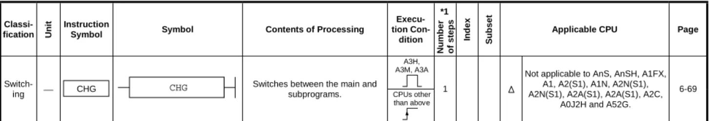
5.5.1 Master control set, reset (MC, MCR) ...5 − 29 5.6 Termination Instructions ...5 − 33 5.6.1 Main routine program termination (FEND) ...5 − 33 5.6.2 Sequence program termination (END) ...5 − 35 5.7 Other Instructions...5 − 37 5.7.1 Sequence program stop (STOP) ...5 − 37 5.7.2 No operation (NOP, NOPLF) ...5 − 39 6. BASIC INSTRUCTIONS...6 −−−− 1 ~ 6 −−−− 89 6.1 Comparison Operation Instructions ...6 − 2 6.1.1 16-bit data comparison (=, <>, >, <=, <, >=)...6 − 4 6.1.2 32-bit data comparison (D=, D<>, D>, D<=, D<,D>=) ...6 − 6 6.2 Arithmetic Operation Instructions...6 − 8 6.2.1 BIN 16-bit addition, subtraction (+, +P, -, -P) ...6 − 10 6.2.2 BIN 32-bit addition, subtraction (D+, D+P, D-, D-P)...6 − 13 6.2.3 BIN 16-bit multiplication, division (*, *P, /, /P) ...6 − 16 6.2.4 BIN 32-bit multiplication, division (D*, D*P, D/, D/P)...6 − 19 6.2.5 BCD 4-digit addition, subtraction (B+, B+P, B-, B-P) ...6 − 22 6.2.6 BCD 8-digit addition, subtraction (DB+, DB+P, DB-, DB-P)...6 − 25 6.2.7 BCD 4-digit multiplication, division (B*, B*P, B/, B/P) ...6 − 28 6.2.8 BCD 8-digit multiplication, division (DB*, DB*P, DB/, DB/P)...6 − 31 6.2.9 16-bit BIN data increment, decrement (INC, INCP, DEC, DECP) ...6 − 34 6.2.10 32-bit BIN data increment, decrement (DINC, DINCP, DDEC, DDECP)...6 − 36 6.3 BCD ↔ BIN Conversion Instructions...6 − 38 6.3.1 BIN data → BCD 4-, 8-digit conversion (BCD, BCDP, DBCD, DBCDP) ...6 − 39 6.3.2 BCD 4-, 8-digit → BIN data conversion (BIN, BINP, DBIN, DBINP) ...6 − 42 6.4 Data Transfer Instructions...6 − 46 6.4.1 16-, 32-bit data transfer (MOV, MOVP, DMOV, DMOVP) ...6 − 47 6.4.2 16-, 32-bit data negation transfer (CML, CMLP, DCML, DCMLP)...6 − 49 6.4.3 16-bit data block transfer (BMOV, BMOVP, FMOV, FMOVP)...6 − 52 6.4.4 16-, 32-bit data exchange (XCH, XCHP, DXCH, DXCHP) ...6 − 56 6.5 Program Branch Instructions ...6 − 58 6.5.1 Conditional jump, unconditional jump (CJ, SCJ, JMP) ...6 − 58 6.5.2 Subroutine call, return (CALL, CALLP, RET)...6 − 62 6.5.3 Interrupt enable, disable, return (EI, DI, IRET) ...6 − 64 6.5.4 Microcomputer program call (SUB, SUBP) ...6 − 67 6.6 Program Switching Instructions ...6 − 69 6.6.1 Main ↔ subprogram switching (CHG)...6 − 69
A − 6
6.7.3 Partial refresh (SEG) ...6 − 87 7. APPLICATION INSTRUCTIONS...7 −−−− 1 ~ 7 −−−− 133 7.1 Logical Operation Instructions ...7 − 2 7.1.1 16-, 32-bit data logical product (WAND, WANDP, DAND, DANDP) ...7 − 3 7.1.2 16-, 32-bit data logical add (WOR, WORP, DOR, DORP)...7 − 7 7.1.3 16-, 32-bit data exclusive logical add (WXOR, WXORP, DXOR, DXORP) ... 7 − 11 7.1.4 16, 32-bit data NOT exclusive logical add (WXNR, WXNRP, DXNR, DXNRP)...7 − 15 7.1.5 BIN 16-bit data 2’s complement (NEG, NEGP) ...7 − 19 7.2 Rotation Instructions ...7 − 21 7.2.1 16-bit data right rotation (ROR, RORP, RCR, PCRP) ...7 − 22 7.2.2 16-bit data left rotation (ROL, ROLR, RCL, RCLP) ...7 − 24 7.2.3 32-bit data right rotation (DROR, DRORP, DRCR, DRCRP)...7 − 26 7.2.4 32-bit data left rotation (DROL, DROLP, DRCL, DRCLP) ...7 − 28 7.3 Shift Instructions ...7 − 30 7.3.1 16-bit data n-bit right shift, left shift (SFR, SFRP, SFL, SFLP) ...7 − 31 7.3.2 n-bit data 1-bit right shift, left shift (BSFR, BSFRP, BSFL, BSFLP) ...7 − 33 7.3.3 n-word data 1-word right shift, left shift (DSFR, DSFRP, DSFL, DSFLP)...7 − 35 7.4 Data Processing Instructions ...7 − 37 7.4.1 16-bit data search (SER, SERP) ...7 − 38 7.4.2 16-, 32-bit data bit check (SUM, SUMP, DSUM, DSUMP) ...7 − 40 7.4.3 8 ↔ 256-bit decode, encode (DECO, DECOP, ENCO, ENCOP)...7 − 42 7.4.4 7 segment decode (SEG) ...7 − 44 7.4.5 Word device bit set, reset (BSET, BSETP, BRST, BRSTP) ...7 − 46 7.4.6 16-bit data dissociation, association (DIS, DISP, UNI, UNIP) ...7 − 48 7.4.7 ASCII code conversion (ASC) ...7 − 51 7.5 FIFO Instructions ...7 − 53 7.5.1 FIFO table write, read (FIFW, FIFWP, FIFR, FIFRP)...7 − 54 7.6 Buffer Memory Access Instructions ...7 − 58 7.6.1 Special function module 1-, 2-word data read (FROM, FROMP, DFRO, DFROP) ...7 − 59 7.6.2 Special function module 1-, 2-word data write (TO, TOP, DTO, DTOP)...7 − 61 7.6.3 Remote terminal module 1- and 2-word data read
(FROM, PRC, FROMP, PRC, DFRO, PRC, DFROP, PRC) ...7 − 63 7.6.4 Remote terminal module 1- and 2-word data write
(TO, PRC, TOP, PRC, DTO, PRC, DTOP, PRC) ...7 − 67 7.6.5 Special module/special block 1-, 2-word data read
(FROM, FROMP, DFRO, DFROP) ...7 − 71 7.6.6 Special module/special block 1-, 2-word data write (TO, TOP, DTO, DTOP)...7 − 74 7.7 FOR to NEXT Instructions ...7 − 77 7.7.1 FOR to NEXT (FOR, NEXT) ...7 − 77
7.9 Display Instructions...7 − 92 7.9.1 ASCII code print instructions (PR, PRC) ...7 − 94 7.9.2 ASCII code comment display instructions (LED, LEDC) ...7 − 100 7.9.3 Character display instructions (LEDA, LEDB) ...7 − 103 7.9.4 Annunciator reset instruction (LEDR) ...7 − 105 7.10 Other Instructions...7 − 108 7.10.1 WDT reset (WDT, WDTP)...7 − 109 7.10.2 Specific format failure check (CHK)... 7 − 111 7.10.3 Status latch set, reset (SLT, SLTR)... 7 − 117 7.10.4 Sampling trace set, reset (STRA, STRAR)... 7 − 119 7.10.5 Carry flag set, reset (STC, CLC)...7 − 121 7.10.6 Pulse regeneration instruction (DUTY) ...7 − 123 7.11 Servo Program Instructions ...7 − 125 7.11.1 Servo program start (DSFRP) ...7 − 126 7.11.2 Present position data and speed change instruction (DSFLP)...7 − 130 8. MICROCOMPUTER MODE ...8 −−−− 1 ~ 8 −−−− 16 8.1 Specifications of Microcomputer Mode...8 − 1 8.2 Using Utility Program ...8 − 2 8.3 Using User-Written Microcomputer Programs...8 − 4 8.3.1 Memory map ...8 − 6 8.3.2 Data memory area address configuration ...8 − 6 8.3.3 Differences in operations called by microcomputer instructions
according to CPU models ...8 − 7 8.3.4 Configuration of data memory area ...8 − 8 9. ERROR CODE LIST...9 −−−− 1 ~ 9 −−−− 41 9.1 Reading Error Codes ...9 − 1 9.2 Error Code List for the An, AnN, A3H, A3M, A3V, A0J2H, AnS, A2C, A73, A52G, A1FX and A3N
board...9 − 1 9.3 Error Code List for AnSHCPU ...9 − 7 9.4 Error Code List for the AnACPU ...9 − 13 9.5 Error Code List for the AnUCPU, A2ASCPU and A2USH board ...9 − 22 9.6 Error Code List for the QCPU-A (A Mode) ...9 − 33 APPENDICES ...APP −−−− 1 ~ APP −−−− 96 APPENDIX 1 LISTS OF SPECIAL RELAYS AND SPECIAL REGISTERS ...APP − 1 1.1 List of Special Relays ...APP − 1 1.2 Special Relays for Link ...APP − 13 1.3 Special Registers ...APP − 16 1.4 Special Registers for Link ...APP − 34
A − 8
Instruction Processing Time of CPUs ...APP − 66 2.3 Instruction Processing Time of QCPU-A (A Mode)...APP − 79 APPENDIX 3 ASCII CODE TABLE...APP − 89 APPENDIX 4 FORMATS OF PROGRAM SHEETS ...APP − 90
1. INTRODUCTION
This manual explains how to use the MELSEC-A series sequence control instructions and microcomputer programs.
MELSEC-A series programmable controllers have a parameter which is used to designate functions and device use ranges.
The functions and device use ranges are determined by the parameter values.
The parameters of CPU are set to default values. If the default can be used for the purpose, it is not necessary to set the parameter.
The user’s programs for the MELSEC-A series PCs are classified as follows.
ACPU Programming Manual (fundamental) gives the programs which can be used for CPUs.
Table 1.1 gives the applicable CPUs the abbreviations used in this manual.
User’s program
Main routine program Subroutine program Interruption program Utility program
User creating
microcomputer program
Main routine program Subroutine program Interruption program User creating
microcomputer program Subsequence
program
Submicrocomputer program
Sequence program
Microcomputer program Main program
Subprogram
1 − 2
Table 1.1 Applicable CPUs and the Abbreviations Used in This Manual
Abbreviations used in this manual Applicable CPUs
A1 A1CPU(P21/R21)
A2(-S1) A2CPU(P21/R21), A2CPU(P21/R21)-S1 An
A3 A3CPU(P21/R21)
A1N A1NCPU(P21/R21)
A2N(-S1) A2NCPU(P21/R21), A2NCPU(P21/R21)-S1 AnN
A3N A3NCPU(P21/R21)
A3H A3HCPU(P21/R21)
A3M A3MCPU(P21/R21)
A3V A3VCPU(P21/R21)
A2A(-S1) A2ACPU(P21/R21), A2ACPU(P21/R21)-S1 AnA
A3A A3ACPU(P21/R21)
A0J2H A0J2HCPU(P21/R21)
A1S A1SCPU, A1SCPU-S1, A1SCPUC24-R2, A1SJCPU, A1SJCPU-S3 AnS
A2S A2SCPU, A2SCPU-S1
A1SH A1SHCPU, A1SJHCPU, A1SJHCPU-S8
AnSH
A2SH A2SHCPU, A2SHCPU-S1
A2C A2CCPU(P21/R21), A2CCPUDC24, A2CCPUC24(-PRF), A2CCPU-S3
A3N board A7BDE-A3N-PT32-S3
A2USH board Type A80BDE-A2USH-S1 PLC CPU Board
A73 A73CPU(P21/R21)
A52G A52GCPU(T21B)
A2U(-S1) A2UCPU, A2UCPU-S1
A3U A3UCPU
AnU
A4U A4UCPU
A2AS(-S1) A2ASCPU, A2ASCPU-S1, A2ASCPU-S30 A2AS
A2USH-S1 A2USHCPU-S1
Q02 Q02CPU-A
Q02H Q02HCPU-A
QCPU-A (A Mode)
Q06H Q06HCPU-A
A1FX A1FXCPU
Abbreviations used in
this manual Peripheral devices
GPP
A6GPP IBM PC/AT(GPP function)
A6HGP A7HGP
A6PHP A7PHPE(GPP function)
POINT
This manual cannot be used in reference to the A0J2CPU(P23/R23).
For the instructions which can be used for the A0J2CPU(P23/R23), refer to the A0J2CPU Programming Manual. (IB-66057)
Table 1.2 Peripheral Devices and the Abbreviations Used in This Manual
Also refer to the following manuals for writing programs for the A series PCs.
Topic Content Reference Manual
CPU specifications
• Memory capacity and the number of devices of the CPU module.
• Specifications of power supply modules, base units, etc.
CPU functions
• System configuration for PC.
• Performance and functions of the CPU module.
• Processings of the CPU module.
• Lists of devices and parameters.
User’s Manual for respective CPU module
Writing programs
• Programming procedures.
• Description of devices and parameters.
• Kinds of programs.
• Configuration of memory areas.
ACPU programming Manual (Fundamentals) IB(NA)-66249
• Description of dedicated instructions (extended application instructions).
AnSHCPU/AnACPU/AnUCPU Programming Manual (Dedicated Instructions) IB(NA)-66251
• Description of the AD57 control instructions. AnACPU/AnUCPU Programming Manual
(AD57 Instructions) IB(NA)-66257 To use A2A(S1)
and A3ACPU
• Description of the PID control instructions. AnACPU/AnUCPU Programming Manual
(PID Instructions.) IB(NA)-66258
To Use A73CPU
• Positioning control.
• Writing servo programs.
• Description of auxiliary and application functions. A73CPU Reference Manual IB(NA)-66233
2 − 1
2. INSTRUCTIONS
2.1 Classification
The instructions of MELSEC-A series are largely classified into sequence instruc- tions, basic instructions, and application instructions. These instructions are shown in Table 2.1.
Table 2.1 Classification of Instructions
Classification of instructions Description page
Contact instruction Operation start, series connection, parallel
connection 5-2 to 5-4
Connection instruction Ladder block connection, operation result
storage/read 5-5 to 5-13
Output instruction Bit device output, pulse output, output reverse 5-14 to 5-26
Shift instruction Bit device shift 5-27 to 5-28
Master control instruction Master control 5-29 to 5-32
Termination instruction Program termination 5-33 to 5-36
Sequence instruction
Other instructions Program stop, no operation, etc. 5-37 to 5-42 Comparison operation instruction Comparison such as =, >, and < 6-2 to 6-7
Arithmetic operation instruction Addition, subtraction, multiplication, and
division of BIN and BCD 6-8 to 6-37 BCD ↔ BIN conversion instruction Conversion from BCD to BIN and BIN to BCD 6-38 to 6-45
Data transfer instruction Transfer of specified data 6-46 to 6-57 Program branch instruction Program jump, subroutine/interrupt program call 6-58 to 6-68 Program switching instruction Switching between main and subprogram 6-69 to 6-81 Basic
instruction
Refresh instruction Link refresh, partial refresh execution 6-82 to 6-88 Logical operation instruction Logical operation such as logical sum and logical
product 7-2 to 7-20
Rotation instruction Rotation of specified data 7-21 to 7-29
Shift instruction Shift of specified data 7-30 to 7-36
Data processing instruction Data processing such as 16-bit data search,
decode, and encode 7-37 to 7-52
FIFO instruction Read/write of FIFO table 7-53 to 7-57
Buffer memory access instruction Data read/write with special function modules and
remote terminals(A2C/A52G). 7-58 to 7-76 FOR to NEXT instruction Program repeated between FOR and NEXT
instruction 7-77 to 7-78
Local, remote I/O station access
instruction Local, remote I/O station data read/write 7-79 to 7-91 Display instruction ASCll code print, character display on LED, etc. 7-92 to 7-107
Others
Instructions which are not included in the above classification, such as WDT reset, and set/reset of
carry flag.
7-108 to 7-124 Application
instruction
Instructions for servo programs Servo program execution and set value change 7-125 to 7-133
2.2 Instruction List
2.2.1 Explanation for instructions lists
Instruction lists in Section 2.2.2 to 2.2.4 are in the following format.
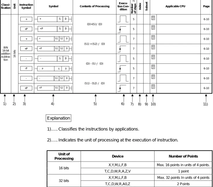
Table 2.2 Explanation for Instructions Lists
Classi-
fication Unit Instruction
Symbol Symbol Contents of Processing
Execu- tion Con-
dition
Number of steps Index Subset Applicable CPU Page
+ 5 ● ● 6-10
+P
(D)+(S)→(D)
5 ● ● 6-10
+ 7 ● ● 6-10
+P
(S1) + (S2) → (D)
7 ● ● 6-10
- 5 ● ● 6-10
-P
(D) - (S) → (D)
5 ● ● 6-10
- 7 ● ● 6-10
BIN 16-bit addition /subtrac tion
16 bits
+P
(S1) - (S2) → (D)
7 ● ● 6-10
Explanation
1)….. Classifies the instructions by applications.
2)….. Indicates the unit of processing at the execution of instruction.
Unit of
Processing Device Number of Points
X,Y,M,L,F,B Max. 16 points in units of 4 points.
16 bits
T,C,D,W,R,A,Z,V 1 point
X,Y,M,L,F,B Max. 32 points In units of 4 points 32 bits
T,C,D,W,R,A0,Z 2 Points
+P S1 S2 D
*1
1) 2) 3) 4) 5) 6) 7) 8) 9) 10) 11)
+ S D
+P S D
+ S1 S2 D
+P S1 S2 D
- S D
- S1 S2 D
- P S D
2 − 3
3)….. Indicates the instruction symbol used for the program. The instruction symbol is shown on a 16-bit instruction basis. The symbols of a 32-bit instruction and an instruction executed only at the rise from OFF to ON are as indicated below:
Instruction executed only at the rise from OFF to ON………P is added to the end of instruction.
4)….. Indicates the symbol diagram in the circuit.
Destination: Indicates the destination of data after operation.
Source: Stores data before operation.
5)….. Indicates the processing of each instruction.
6)….. Indicates the execution condition of each instruction and details are as described below:
Symbol Execution Condition
32-bit instruction………D is added to the head of instruction.
+ D +
Example:
16-bit instruction 32-bit instruction
Example: + +P
Instruction executed
during ON Instruction executed only
at the rise from OFF to ON
+ S D
Indicates destination.
Indicates source.
Indicates instruction symbol.
Indicates destination.
Indicates source.
Indicates instruction symbol.
+ S1 S2 D
Fig. 2.2 Symbol Representations in Ladder
(D) + (S) → (D)
Indicates 16 bits.
(D + 1, D) + (S + 1, S) → (D + 1, D) 16 bits, 16 bits
Indicates 32 bits.
Upper 16 bits Lower 16 bits
D + 1 D
Fig. 2.3 Processing of Each Instruction
No entry Instruction which is always executed regardless of ON/OFF of the preceding condition.
If the preceding condition is OFF, that instruction executes an OFF processing.
Instruction which is executed during ON. Executes instruction only while the preceding condition of that instruction is on. When the preceding condition is off, that instruction is not executed and not processed.
Instruction which is executed once during ON. Executes instruction only at the positive transition of the preceding condition of instruction, i.e. the condition changes from off to on. Thereafter, even if the condition is on, that instruction is not executed and not processed.
Instruction which is executed once during OFF. Executes instruction only at the negative transition of the preceding condition of instruction, i.e. the condition changes from on to off. Thereafter, even is the condition is off, that instruction is not executed and not processed.
7)….. Indicates the number of steps of each instruction. The number of steps, which change depending on conditions, is indicated in two stages. For details, refer to each instruction.
POINT
If extension devices are used or index qualification is performed with bit devices in the case of the instructions which need device specification for the AnA, A2AS, AnU, QCPU-A (A Mode) and A2USH board, the number of steps increases. Refer to Section 3.8.1 for details.
8)….. The ● mark indicates that the instruction can be indexed (Z, V).
The mark indicates that the instruction can be indexed with the AnA, A2AS, AnU, QCPU-A (A Mode) and A2USH board only.
9)….. The ● mark indicates that the instruction is a subset instruction.
The mark indicates that the subset processing can be performed with the A3H, A3M, AnA, A2AS, AnU, QCPU-A (A Mode) and A2USH board only.
10)… Indicates applicable CPU.
The ! mark indicates that it is applicable to all types of CPUs.
The mark indicates that it is applicable to some types of CPUs.
The mark indicates that it is applicable to specific CPUs.
11).... Indicates a page which explains each instruction.
2 − 5 2.2.2 Sequence instructions
(1) Contact instructions
Table 2.3 Contact Instructions
Classi-
fication Unit Instruction
Symbol Symbol Contents of Processing
Execu- tion Con-
dition
Number of steps Index Subset
Applicable CPU Page
LD Logical operation start
(NO contact operation start) 1 ! 5-2
LDI Logical NOT operation start
(NC contact operation start) 1 ! 5-2
AND Logical product
(NO contact series connection) 1 ! 5-2
ANI Logical product NOT
(NC contact series connection) 1 ! 5-2
OR Logical add
(NO contact parallel connection) 1 ! 5-2
Contact
ORI Logical add NOT
(NC contact parallel connection) 1 ! 5-2
(2) Connection instructions
Table 2.4 Connection Instructions
Classi-
fIcation Unit Instruction
Symbol Symbol Contents of Processing
Execu- tion Con-
dition
Number of steps Index Subset Applicable CPU Page
ANB ANDs logical blocks.
(Series connection of blocks) 1 ! 5-5
ORB Ors logical blocks.
(Parallel connection of blocks) 1 ! 5-5
MPS Stores the operation result. 1 ! 5-9
MRD Reads the operation result
from MPS 1 ! 5-9
Connec- tion
MPP Reads the operation result from
MPS and clears the result. 1 ! 5-9
*1: For the number of steps when extension devices are used or when index qualification is performed to bit devices for AnA, A2AS, AnU, QCPU-A (A Mode) and A2USH board, refer to Section 3.8.1.
*2: The mark in the Index column indicates that index qualification can be performed with the AnA, A2AS, AnU, QCPU-A (A Mode) and A2USH board only.
*3: The mark in the Subset column indicates that subset processing can be performed with the A3H, A3M, AnA, A2AS, AnU, QCPU-A (A Mode) and A2USH board only.
MPS
MRD
MPP
*2
*2
*2
*2
*2
*2
*1
*1
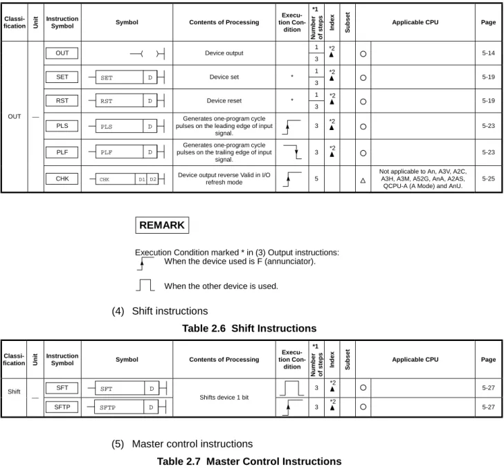
(3) Output instructions
Table 2.5 Output instructions
Classi-
fication Unit Instruction
Symbol Symbol Contents of Processing
Execu- tion Con-
dition
Number of steps Index Subset
Applicable CPU Page
1
OUT Device output
3 ! 5-14
1
SET Device set *
3 ! 5-19
1
RST Device reset *
3 ! 5-19
PLS
Generates one-program cycle pulses on the leading edge of input
signal.
3 ! 5-23
PLF
Generates one-program cycle pulses on the trailing edge of input
signal.
3 ! 5-23
OUT
CHK Device output reverse Valid in I/O
refresh mode 5
Not applicable to An, A3V, A2C, A3H, A3M, A52G, AnA, A2AS,
QCPU-A (A Mode) and AnU.
5-25
REMARK
Execution Condition marked * in (3) Output instructions:
When the device used is F (annunciator).
When the other device is used.
(4) Shift instructions
Table 2.6 Shift Instructions
Classi-
fication Unit Instruction
Symbol Symbol Contents of Processing
Execu- tion Con-
dition
Number of steps Index Subset
Applicable CPU Page
SFT 3 ! 5-27
Shift
SFTP
Shifts device 1 bit
3 ! 5-27
(5) Master control instructions
Table 2.7 Master Control Instructions
Classi-
fication Unit Instruction
Symbol Symbol Contents of Processing
Execu- tion Con-
dition
Number of steps Index Subset Applicable CPU Page
MC Master control start 5 ! 5-29
Master control
MCR Master control reset 3 ! 5-29
*1: For the number of steps when extension devices are used or when index qualification is performed to bit devices for AnA, A2AS, AnU, QCPU-A (A Mode) and A2USH board, refer to Section 3.8.1.
*2: The mark in the Index column indicates that index qualification can be performed with the AnA, A2AS, AnU, QCPU-A (A Mode) and A2USH board only.
*3: The mark in the Subset column indicates that subset processing can be performed with the A3H, A3M, AnA, A2AS, AnU, QCPU-A (A Mode) and A2USH board only.
SET D
*2
*2
*2
*2
*2
*2
*2
RST D
PLS D
PLF D
CHK D1 D2
*1
*1
*2
SFT D
SFTP D
*1
MC n D
MCR n
2 − 7 (6) Termination instructions
Table 2.8 Termination Instructions
Classi-
fication Unit Instruction
Symbol Symbol Contents of Processing
Execu- tion Con-
dition
Number of steps Index Subset
Applicable CPU Page
FEND
Always used at the end of the main routine program to terminate processing.
1 ! 5-33
Program end
END Always used at the end of the
sequence program to return to step 0.
1 ! 5-35
(7) Other instructions
Table 2.9 Other Instructions
Classi-
fication Unit Instruction
Symbol Symbol Contents of Processing
Execu- tion Con-
dition
Number of steps Index Subset Applicable CPU Page
Stop STOP
Resets output after the input condition is enabled, and stops the sequence program. The sequence program is resumed by setting the
RUN key switch to RUN.
1 ! 5-37
No opera-
tion
NOP No operation
For program erasure or space 1 ! 5-39
*1: For the number of steps when extension devices are used or when index qualification is performed to bit devices for AnA, A2AS, AnU, QCPU-A (A Mode) and A2USH board, refer to Section 3.8.1.
*2: The mark in the Index column indicates that index qualification can be performed with the AnA, A2AS, AnU, QCPU-A (A Mode) and A2USH board only.
*3: The mark in the Subset column indicates that subset processing can be performed with the A3H, A3M, AnA, A2AS, AnU, QCPU-A (A Mode) and A2USH board only.
STOP
*1
*1 FEND
2.2.3 Basic instructions
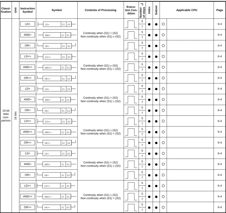
(1) Comparison instructions
Table 2.10 Comparison Operation Instructions (Continue)
Classi-
fication Unit Instruction
Symbol Symbol Contents of Processing
Execu- tion Con-
dition
Number of steps Index Subset
Applicable CPU Page
5 LD=
7 ● ● ! 6-4
5 AND=
7 ● ● ! 6-4
5 OR=
Continuity when (S1) = (S2) Non-continuity when (S1) ≠ (S2)
7 ● ● ! 6-4
5 LD<>
7 ● ● ! 6-4
5 AND<>
7 ● ● ! 6-4
5 OR<>
Continuity when (S1) ≠ (S2) Non-continuity when (S1) = (S2)
7 ● ● ! 6-4
5 LD>
7 ● ● ! 6-4
5 AND>
7 ● ● ! 6-4
5 OR>
Continuity when (S1) > (S2) Non-continuity when (S1) ≤ (S2)
7 ● ● ! 6-4
5 LD<=
7 ● ● ! 6-4
5 AND<=
7 ● ● ! 6-4
5 OR<=
Continuity when (S1) ≤ (S2) Non-continuity when (S1) > (S2)
7 ● ● ! 6-4
5 LD<
7 ● ● ! 6-4
5 AND<
7 ● ● ! 6-4
5 OR<
Continuity when (S1) < (S2) Non-continuity when (S1) ≥ (S2)
7 ● ● ! 6-4
5 LD>=
7 ● ● ! 6-4
5 AND>=
7 ● ● ! 6-4
5 16-bit
data com- parison 16 bits
OR>=
Continuity when (S1) ≥ (S2) Non-continuity when (S1) < (S2)
7 ● ● ! 6-4
*1: For the number of steps when extension devices are used or when index qualification is performed to bit devices for AnA, A2AS, AnU, QCPU-A (A Mode) and A2USH board, refer to Section 3.8.1.
*2: The mark in the Index column indicates that index qualification can be performed with the AnA, A2AS, AnU, QCPU-A (A Mode) and A2USH board only.
*3: The mark in the Subset column indicates that subset processing can be performed with the A3H, A3M, AnA, A2AS, AnU, QCPU-A (A Mode) and A2USH board only.
*1
LD= S1 S2
AND= S1 S2
OR= S1 S2
LD<> S1 S2
AND<> S1 S2
OR<> S1 S2
LD> S1 S2
AND> S1 S2
OR> S1 S2
LD<= S1 S2
AND<= S1 S2
OR<= S1 S2
LD< S1 S2
AND< S1 S2
OR< S1 S2
AND>= S1 S2
OR>= S1 S2 LD>= S1 S2
2 − 9
Table 2.10 Comparison Operation Instructions
Classi-
fication Unit Instruction
Symbol Symbol Contents of Processing
Execu- tion Con-
dition
Number of steps Index Subset
Applicable CPU Page
LDD= 11 ● ! 6-6
ANDD= 11 ● ! 6-6
ORD=
Continuity when (S1+1, S1)
= (S2+1, S2) Non-continuity when (S1+1, S1)
≠ (S2+1, S2)
11 ● ! 6-6
LDD<> 11 ● ! 6-6
ANDD<> 11 ● ! 6-6
ORD<>
Continuity when (S1+1, S1)
≠ (S2+1, S2) Non-continuity when (S1+1, S1)
= (S2+1, S2)
11 ● ! 6-6
LDD> 11 ● ! 6-6
ANDD> 11 ● ! 6-6
ORD>
Continuity when (S1+1, S1)
> (S2+1, S2) Non-continuity when (S1+1, S1)
≤ (S2+1, S2)
11 ● ! 6-6
LDD<= 11 ● ! 6-6
ANDD<= 11 ● ! 6-6
ORD<=
Continuity when (S1+1, S1)
≤ (S2+1, S2) Non-continuity when (S1+1, S1)
> (S2+1, S2)
11 ● ! 6-6
LDD< 11 ● ! 6-6
ANDD< 11 ● ! 6-6
ORD<
Continuity when (S1+1, S1)
< (S2+1, S2) Non-continuity when (S1+1, S1)
≥ (S2+1, S2)
11 ● ! 6-6
LDD>= 11 ● ! 6-6
ANDD>= 11 ● ! 6-6
32 bit data com- parison 32 bits
ORD>=
Continuity when (S1+1, S1)
≥ (S2+1, S2) Non-continuity when (S1+1, S1)
< (S2+1, S2)
11 ● ! 6-6
*1: For the number of steps when extension devices are used or when index qualification is performed to bit devices for AnA, A2AS, AnU, QCPU-A (A Mode) and A2USH board, refer to Section 3.8.1.
*2: The mark in the Index column indicates that index qualification can be performed with the AnA, A2AS, AnU, QCPU-A (A Mode) and A2USH board only.
*3: The mark in the Subset column indicates that subset processing can be performed with the A3H, A3M, AnA, A2AS, AnU, QCPU-A (A Mode) and A2USH board only.
LDD= S1 S2
ANDD= S1 S2
ORD= S1 S2
LDD<> S1 S2
ANDD<> S1 S2
ORD<> S1 S2
LDD> S1 S2
ANDD> S1 S2
ORD> S1 S2
LDD<= S1 S2
ANDD<= S1 S2
ORD<= S1 S2
*1
LDD< S1 S2
ANDD< S1 S2
ORD< S1 S2
LDD>= S1 S2
ANDD>= S1 S2
ORD>= S1 S2
(2) Arithmetic operation instruction
Table 2.11 Arithmetic Operation Instruction (Continue)
Classi-
fication Unit Instruction
Symbol Symbol Contents of Processing
Execu- tion Con-
dition
Number of steps Index Subset
Applicable CPU Page
+ 5 ●●●● ●●●● ! 6-10
+P
(D) + (S) → (D)
5 ●●●● ●●●● ! 6-10
+ 7 ●●●● ●●●● ! 6-10
+P
(S1) + (S2) → (D)
7 ●●●● ●●●● ! 6-10
- 5 ●●●● ●●●● ! 6-10
-P
(D) - (S) → (D)
5 ●●●● ●●●● ! 6-10
- 7 ●●●● ●●●● ! 6-10
BIN 16-bit addition/
subtrac- tion
16 bits
-P
(S1) - (S2) → (D)
7 ●●●● ●●●● ! 6-10
D+ 9 ●●●● ●●●● ! 6-13
D+P
(D+1, D) + (S+1, S)
→ (D+1, D)
9 ●●●● ●●●● ! 6-13
D+ 11 ●●●● ●●●● ! 6-13
D+P
(S1+1, S1) + (S2+1, S2)
→ (D+1, D)
11 ●●●● ●●●● ! 6-13
D- 9 ●●●● ●●●● ! 6-13
D-P
(D+1, D) - (S+1, S) → (D+1, D)
9 ●●●● ●●●● ! 6-13
D- 11 ●●●● ●●●● ! 6-13
BIN 32bit addition/
subtrac- tion
32 bits
D-P
(S1+1, S1) - (S2+1, S2)
→ (D+1, D)
11 ●●●● ●●●● ! 6-13
∗ 7 ●●●● ●●●● ! 6-16
∗P
(S1) × (S2) → (D+1, D)
7 ●●●● ●●●● ! 6-16
/ 7 ●●●● ●●●● ! 6-16
BIN 16bit multipli-
cation/
division
16 bits
/P
(S1) / (S2) → Quotient (D), Remainder (D+1)
7 ●●●● ●●●● ! 6-16
*1: For the number of steps when extension devices are used or when index qualification is performed to bit devices for AnA, A2AS, AnU, QCPU-A (A Mode) and A2USH board, refer to Section 3.8.1.
*2: The mark in the Index column indicates that index qualification can be performed with the AnA, A2AS, AnU, QCPU-A (A Mode) and A2USH board only.
*3: The mark in the Subset column indicates that subset processing can be performed with the A3H, A3M, AnA, A2AS, AnU, QCPU-A (A Mode) and A2USH board only.
*1
* S1 S2 D
+ S D
+P S D
+ S1 S2 D
+P S1 S2 D
- S D
- P S D
- S1 S2 D
- P S1 S2 D
D+ S D
D+ S1 S2 D
D+ P S D
D+ P S1 S2 D
D- S D
D- P S D
D- S1 S2 D
D-P S1 S2 D
/ S1 S2 D
/ P S1 S2 D
*P S1 S2 D
2 − 11
Table 2.11 Arithmetic Operation Instruction (Continue)
Classi-
fication Unit Instruction
Symbol Symbol Contents of Processing
Execu- tion Con-
dition
Number of steps Index Subset
Applicable CPU Page
D∗ 11 ● ● ! 6-19
D∗P
(S1+1, S1) × (S2+1, S2)
→ (D+3, D+2, D+1, D)
11 ● ● ! 6-19
D/ 11 ● ● ! 6-19
BIN 32bit multipli-
cation/
division
32 bits
D/P
(S1+1, S1) / (S2+1, S2) → Quotient (D+1, D), Remainder (D+3, D+2)
11 ● ● ! 6-19
B+ 7 ● ! 6-22
B+P
(D) + (S) → (D)
7 ● ! 6-22
B+ 9 ● ! 6-22
B+P
(S1) + (S2) → (D)
9 ● ! 6-22
B- 7 ● ! 6-22
B-P
(D) - (S) → (D)
7 ● ! 6-22
B- 9 ● ! 6-22
BCD 4-digit addition/
subtrac-
tion BCD 4-digits
B-P
(S1) - (S2) → (D)
9 ● ! 6-22
DB+ 9 ● ! 6-25
DB+P
(D+1, D) + (S+1, S)
→ (D+1, D)
9 ● ! 6-25
DB+ 11 ● ! 6-25
BCD 8-digit addition subtrac-
tion BCD 8-digits
DB+P
(S1+1, S1) + (S2+1, S2))
→ (D+1, D)
11 ● ! 6-25
DB- 9 ● ! 6-25
DB-P
(D+1, D) - (S+1, S)
→ (D+1, D)
9 ● ! 6-25
DB- 11 ● ! 6-25
BCD 8-digit addition, subtrac-
tion BCD 8-digits
DB-P
(S1+1, S1) - (S2+1, S)
→ (D+1, D)
11 ● ! 6-25
*1: For the number of steps when extension devices are used or when index qualification is performed to bit devices for AnA, A2AS, AnU, QCPU-A (A Mode) and A2USH board, refer to Section 3.8.1.
*2: The mark in the Index column indicates that index qualification can be performed with the AnA, A2AS, AnU, QCPU-A (A Mode) and A2USH board only.
*3: The mark in the Subset column indicates that subset processing can be performed with the A3H, A3M, AnA, A2AS, AnU, QCPU-A (A Mode) and A2USH board only.
*1
*3
*3
*3
*3
D/ S1 S2 D
D/ P S1 S2 D
B+ S D
B+P S D
B+ S1 S2 D
B+P S1 S2 D
B- S D
B-P S D
B- S1 S2 D
B- P S1 S2 D
DB+ S D
DB+P S D
DB+ S1 S2 D
DB+P S1 S2 D
DB- S D
DB- P S D
DB- S1 S2 D
DB- P S1 S2 D
D* S1 S2 D
D P* S1 S2 D