Class D Series Resonant Converter Controlled with FPGA-Based Delta-Sigma Modulator
Hirotaka Koizumi
Department of Electrical Engineering Tokyo University of Science Chiyoda-ku, Tokyo 102-0073 JAPAN
E-mail: [email protected]
Abstract—A 1st order 1-bit delta-sigma modulator to control a Class D series resonant converter is built with an FPGA. The target reference and the feedback gain are freely chosen. A Class D series resonant converter designed at an operating frequency of 200 [kHz] was built and driven by the FPGA-based delta-sigma modulator. Maintaining zero-current switching (ZCS) operation, the output voltage and power were changed from 0.945 [V], 89.1 [mW] to 8.22 [V], 6.75 [W] in the circuit experiments fed by 20.0 [V] dc-voltage source. The measured power conversion efficiency was from 71.8 [%] to 83.0 [%]. These performances have also been confirmed with MATLAB simulink simulator. In the frequency domain, no specific component was found except the switching frequency and its 2nd harmonic in the observed output voltage.
Keywords—Class D; resonant converter; delta-sigma modula- tion.
I. INTRODUCTION
In series resonant converters, the zero-current switching (ZCS) or the zero-voltage switching (ZVS) can be maintained when the switching frequency is equal to the resonant fre- quency [1]-[5]. Therefore, the periodical 1-bit output signal of a 1-bit delta-sigma modulator is suitable for regulating the output power/voltage. These days, integrated circuits (ICs) of delta-sigma modulators, which are designed for digital audio amplifiers or switching power converters, are widely in the market [6][7]. For instance, a 1-bit delta-sigma mod- ulator PCM4202[6] is applied to the Class D series resonant converter[5]. However, all the inner parameters of a ready- made IC are not always opened. Therefore one has to use an IC as a black box without knowing the primary characteristics.
To make it clear the effect of the feedback gain and the order of delta-sigma modulation on the Class D series resonant con- verter, a 1-bit delta-sigma modulator with adjustable function of the inner parameters is required.
In this study, a 1st order 1-bit delta-sigma modulator to control a Class D series resonant converter is built with an FPGA (Cyclone EP1C6T144C8N). The target reference and the feedback gain are freely chosen. The 1-bit output signal is generated to drive a Class D series resonant converter. An experimental circuit was designed and built at the operating frequency of 200 [kHz], which was driven by the FPGA-based
This study is supported by Japan Society for the Promotion of Science Grant-in-Aid for Scientific Research C 20560278.
S
3S
5S
4S
6v
oC
fS
1S
2V
II
Iv
S2v
S1i
S2i
S1L C
i
ov
Lv
C+ -
Class D ZCS series
resonant inverter Full-wave rectifier
R
LV
oFig. 1. Delta-sigma modulated Class D series resonant converter.
delta-sigma modulator. Maintaining ZCS operation, the output voltage and power were changed from 0.945 [V], 89.1 [mW]
to 8.22 [V], 6.75 [W] in the circuit experiments fed by a 20.0 [V] dc-voltage source, where the measured power conversion efficiency was from 71.8 [%] to 83.0 [%]. These performances have also been confirmed with MATLAB simulink simulator.
In the frequency domain, no specific component was found except the switching frequency and its 2nd harmonic in the output voltage observed with the FFT function equipped with the digital oscilloscope. The other components are generally less than -20 [dBV].
II. CIRCUITDESCRIPTION
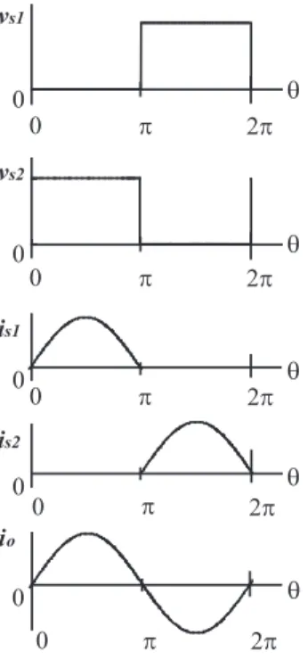
A Class D series resonant converter is shown in Fig. 1, which is composed of a Class D ZCS series resonant inverter and a full-wave rectifier[1]. Two active switchesS1andS2are alternatively turned on and off; thus the switch voltages vS1 andvS2 alternatively take zero and the input voltageVi by a half period as shown in Fig. 2. The square voltage waveform of vS2is given for theL − C series resonant circuit. Assuming a high loaded quality factorQLof the series resonant circuit, the
Fig. 2. Waveforms in Class D ZCS series resonant inverter.
current io becomes sinusoidal. When the resonant frequency is designed to be equal to the switching frequency, ZCS is achieved. Besides, in the case when the switching frequency is higher than the resonant frequency, ZVS is achieved with the intrinsic body diode of the MOSFET, which leads to high efficient power conversion with low switching noise [1]. As shown in Fig. 2, the current io flows through S1 and S2
as iS1 and iS2 by a half period. The switching transition occurs at the zero current instant. When the inverter is loaded with a full-wave rectifier, the load resistance RL performs as an equivalent resistance Ri = 8RL/π2 [1]. Through the diodes S3toS6, a dc-output voltageVo is obtained, which is approximately 0.5Vi [1].
III. REGULATIONMETHOD
As a regulation method, pulse density modulation (PDM) has been getting more popular as the digital control has been spreading. In PDM the switch-on term and the switch-off term is periodically changed at the fixed switching frequency.
Therefore, switching condition (ZCS/ZVS) is maintained [2]- [4] when PDM is applied to resonant power converters which satisfy the condition that the resonant frequency is equal to the switching frequency. Two drawbacks of PDM are the sub- harmonics and the discontinuity of the output power/voltage, which are caused by predetermined switching patterns. The delta-sigma modulation [7], which doesn’t need any switching patterns, is effective for these problems. Fig. 3 shows a block diagram of a 1st order 1 bit delta-sigma modulator [7]. A reference x1 is given as an input signal. The signal x2 to the integrator takes x1 − G to x1+ G, because the output value of the quantizerx4is -1 for a negative value, 1 for zero or a positive value. While x4 is 1, the switches S1 and S2
Quantizer +
-
Z
-1G
x
2Z-1 x
3x
4x
1Fig. 3. A block diagram of a 1st order delta-sigma modulator.
of the converter shown in Fig.1 periodically repeat normal switching. While x4 is -1, S1 stays off, and S2 stays on, then the amplitude of the currentio is getting smaller during this term. The output power/voltage can be controlled with the damping phenomenon almost continuously with low sub- harmonics [5].
This is obvious by Fig. 3,x4 is affected by the structure of the delta-sigma modulator and the feedback gainG, which are not always opened when one uses a ready-made delta-sigma modulation IC. To make it clear how the inner parameters and the structure of a delta-sigma modulator affects the performance of a resonant converter controlled with the delta- sigma modulator, an FPGA-based delta-sigma modulator is needed. In this study, a 1st order 1-bit delta-sigma modulator is built with an FPGA.
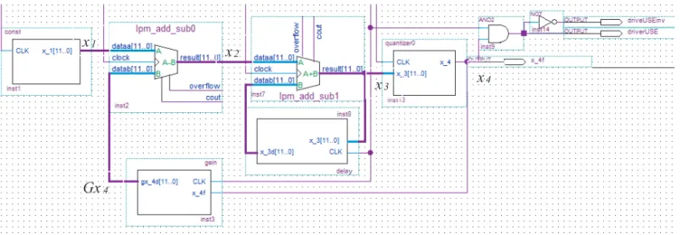
A screen copy of a designed file of the 1st order 1-bit delta-sigma modulator with Altera Quartus II is shown in Fig. 4. The fundamental structure is modelled after the block diagram in Fig. 3. For the parametersx1tox3, andGx4, 12-bit integers are assigned, where the 1st bit shows plus/minus. The output signalx4 has 1 bit. This time, the input referencex1 is numerically given as an integer. Different from the model of Fig. 3,x4takes 0 for a negative value ofx3, otherwise 1. Then, Gx4 takes G for x4 = 1 otherwise −G. When x1 = G, x4
keeps 1. Whenx1= −G, x4keeps 0. Between−G and G, the referencex1can be freely chosen. The largerG leads to finely- tuned regulation. The fundamental clock 200 [kHz], which is equal to the switching frequency of the resonant converter, is made from 30 [MHz] from the original clock of the FPGA.
A small delay is given between the clocks for each block.
Considering the calculation time, the gate driving signals for S1 and S2 are given through an AND gate from x4 and a delayed clock signal.
IV. EXPERIMENTALRESULTS
A Class D series resonant converter is designed at the switching frequencyfs= 200 [kHz]. The followings are given as a circuit design; the input voltage Vi = 20.0 [V], the load resistance RL = 10 [Ω], the loaded quality factor QL
= 5, and the switching frequency fs = 200 [kHz] which is equal to the resonant frequency. The resonant inductance L and capacitance C are calculated by L = QLRi/ωs, and C = 1/ωs2L = 1/ωsQLRi, where ωs = 2πfs is a switching angular frequency, and Ri = 0.81RL is an equivalent resis- tance of the rectifier [1]. The designed and measured values of
x
1x
2x
3x
4Gx
4Fig. 4. A designed block diagram of the FPGA-based 1st order 1-bit output delta-sigma modulator.
TABLE I
THEDESIGNED ANDMEASUREDVALUES OFTHECIRCUITELEMENTS.
L [µH] C [nF] RL[Ω]
Designed 32.3 19.6 10.0
Measured 32.0 19.7 10.0
ESR[mΩ] 360 170 -
the circuit elements are shown in Table I, where ESR means the measured equivalent series resistance. A 470 [μF] filter capacitor is used forCf. Its measured values were 430 [μF]
with ESR of 185 [mΩ] at 200 [Hz] and 4.48 [μF] with ESR of 126 [mΩ] at 200 [kHz]. MOSFET’s IRF510 are used for the switchesS1andS2. Schottky barrier diodes SR340 (Rectron) are used for the switches S3 to S6. Using these devices, a Class D series resonant converter was built and tested. The driving signals were given from the FPGA-based delta-sigma modulator (Cyclone EP1C6T144C8N), where the feed-back gain G = 15 was set. The reference value x1 was changed from -15 to 15. The relationship between the reference x1 and the output voltage Vo is shown in Fig. 5. In these tests, the output voltage Vo was changed from 0.945 [V] at x1 = -13 to 8.22 [V] at x1 = 15. At x1 = -15, Vo was 0. A linear approximationVo= 0.264 × x1+ 4.12 can be drawn in Fig.
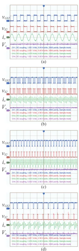
5. Corresponding to the output voltage, the output power was changed from 89.1 [mW] to 8.22 [W] at 200.0 [kHz], where the measured power conversion efficiency was 71.8 [%] and 83.0 [%]. The four observed waveforms are shown in Fig. 6, where vGS2 is the gate driving voltage for S2. As shown in Fig. 6 (a), normal switching was repeated forx1 = 15. Figs.
6 (b) to (d) were respectively observed when x1 = 7, 0, and -7 were given. While the complex driving patterns generated by the delta-sigma modulator were observed in Fig. 6 (b) and (d), a periodical driving pattern was also observed as shown in Fig. 6 (c). In Fig. 6 the current io flowing through the resonant circuit crosses over zero at the switching instant for
0 5 10
-15 -10 -5 0 5 10 15 Output
voltage [V]
Reference value
Fig. 5. The relation ship between the reference value and the output voltage Vo.
each waveform.
A delta-sigma modulator and the Class D series resonant converter was built with MATLAB Simulink under the same designed conditions to the circuit experiments. Giving the same feed-back gainG and the reference x1, the currentio, the output voltageVo, and the switch voltagevS2were calculated as shown in Fig. 7. Judging fromvS2, the same driving patterns to the FPGA-based delta-sigma modulator were generated, which mean that the FPGA-based deltasigma modulator oper- ated as intended. The other calculated waveforms are also in accordance with the experimental results. In each waveform, the currentio crosses over zero at the switching instant.
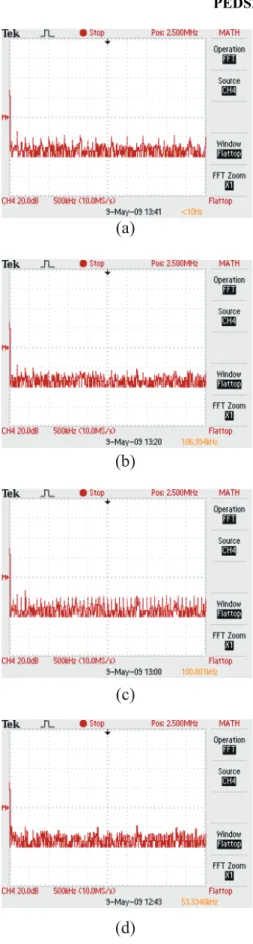
In the circuit experiments, the output voltage Vo was also observed with the FFT function equipped with the digital oscilloscope. Fig. 8 shows the spectra corresponding to Fig.
6 (a) to (d). In Fig. 8 (b) and (d), the observed spectra are
corresponding to Fig. 6 (c) and Fig. 7 (c), more spectra are observed than the other three. However each amplitude is not higher than the spectrum observed in Fig. 8 (a). Common to all spectra, no specific component was found except for the switching frequency fs at 200 [kHz] and its 2nd harmonic.
The other components are generally less than -20 [dBV].
V. CONCLUSION
A 1st order 1-bit delta-sigma modulator to control a Class D series resonant converter has been built with an FPGA.
The reference value and the feedback gain are freely chosen, which are important for the future research for evaluating the performance of resonant converters controlled with a delta- sigma modulator. A Class D series resonant converter designed at operating frequency of 200 [kHz] was designed, built, and driven by the FPGA-based delta-sigma modulator. With a maintaining ZCS, high-efficiency and wide-range dc/dc power conversion have been confirmed in circuit experiments. These performances have been also confirmed in the simulation with MATLAB simulink simulator. In the frequency domain, no specific component was found, except for the switching frequency and its 2nd harmonic in the observed output voltage.
REFERENCES
[1] M. K. Kazimierczuk, D. Czarkowski, “Resonant Power Converters,”
Willey-Interscience, N.Y. 1995.
[2] H. Fujita, and H. Akagi, “Pulse-density-modulated power control of a 4 kW, 450kHz voltage-source inverter for induction melting application,”
IEEE Trans. Ind. Appl., vol. 32, no. 2 pp. 279–286, Mar./Apr. 1996.
[3] H. Koizumi, K. Kurokawa, and S. Mori, “Analysis of Class D inverter with irregular driving patterns,” 1-bit delta-sigma modulator to control IEEE Trans. on Circuits and Syst., Part-I: Regular Papers, vol. 53, no.
3, pp. 677-687, Mar. 2006.
[4] Nam-Ju Park, Dong-Yun Lee, Dong-Seok Hyun, “A power-control scheme with constant switching frequency in Class-D inverter for induction-heating jar application,” IEEE Trans. Ind. Elec., vol. 54, no. 3 pp. 1252-1260, June 2007.
[5] H. Koizumi, ”Delta-sigma modulated Class D series resonant converter,”
in Proc. IEEE Power Electronics Specialists Conference, 2008, pp. 257- 262, June 2008.
[6] Texas Instruments Incorporated,“PCM4202EVM User’s Guide,” [Online].
Available: http://focus.ti.com/lit/ug/sbau103/sbau103.pdf
[7] K. Masuda, T. Hayase, S. Satoh, “1 bit audio,” Sharp Tech. Report, vol.
77, pp. 67-72, Aug. 2000 (in Japanese).
v
S2i
oV
ov
GS2v
S2i
oV
ov
GS2v
S2i
oV
ov
GS2v
S2i
oV
ov
GS2(a)
(b)
(c)
(d)
Fig. 6. Observed waveforms: (a)x1 = 15, (b)x1 = 7, (c)x1 = 0, and (d) x1= -7. Vertical 10 V/div forvGS2, 20 V/div forvS2, 2 A/div forioin (a) and (b), 1 A/div forioin (c) and (d), 10 V/div forVo in (a) and (b), and 5 V/div forVoin (c) and (d); horizontal: 5µsec/div in (a), 25 µsec/div in (b) to (d).
vS2 [V]io [A]Vo [V]
Time [s]
(d) (c) vS2 [V]io [A]Vo [V]
Time [s]
(b) vS2 [V]io [A]Vo [V]
Time [s]
vS2 [V]io [A]Vo [V]
Time [s]
(a)
Fig. 7. Calculated waveforms with MATLAB Simulink simulation; from the top, inverter currentio, output voltageVo, and switch voltagevS2, (a)x1= 15, (b)x1= 7, (c)x1= 0, and (d)x1 = -7.
(d) (c) (b) (a)
Fig. 8. Spectra of the output voltage waveformsVo observed in frequency domain with the FFT function of the digital oscilloscope: vertical 20 dbV/div, horizontal: 500 kHz/div. (a)x1= 15, (b)x1= 7, (c)x1 = 0, and (d)x1 = -7.