GaN-Based Ultraviolet p-i-n Photodiodes with Buried p-Layer
Structure Grown by MOVPE
M. L. Leeaand J. K. Sheub,z a
Department of Electro-Optical Engineering, Southern Taiwan University of Technology, Yung-Kang City, Tainan 710, Taiwan
b
Institute of Electro-Optical Science and Engineering, National Cheng Kung University, Tainan 70101, Taiwan
The following study presents an analysis of AlGaN/GaN p-i-n photodiode, which was designed with a buried p+-GaN layer
combining a heavy doped n++-In
0.3Ga0.7N layer in order to form a p+/n++tunneling junction under the AlGaN/GaN n-i-p
hetero-structure. Compared to the conventional AlGaN-based p-i-n photodiodes, the inverted devices are capable of low-resistivity and high aluminum-containing n-type AlGaN top contact layer. The inverted devices exhibited a typical unbiased peak responsivity of 0.1 A/W at 350 nm corresponding to a quantum efficiency of around 35%. The unbiased rejection ratio was about four orders of magnitude over the ultraviolet and visible regions of the spectrum. The typical dark current density of the inverted devices was below 5 nA/cm2at the reverse bias below 2 V.
© 2007 The Electrochemical Society. 关DOI: 10.1149/1.2426889兴 All rights reserved.
Manuscript submitted March 29, 2006; revised manuscript received October 10, 2006. Available electronically January 16, 2007.
GaN-based metal-semiconductor-metal共MSM兲 photodetectors,1 p-i-n photodiodes共PDs兲,2,3and Schottky barrier detectors,4that op-erate in the UV region, have all been demonstrated. All of the afore-mentioned UV detectors can potentially find application in a variety of areas, including solar astronomy, missile detection, combustion process monitors, flame sensors, and space-to-space communica-tions.5-8 However, some fundamental problems put limits on the performance of AlGaN-based solar-blind p-i-n photodiodes. In tra-ditional designs, n- and p-type layers have a larger bandgap than the absorbing layer sandwiched between them. As aluminum content of an AlGaN layer increases, cracking occurs, resulting in a large dark current and a correspondingly low detectivity. The p-type AlGaN layer must feature a high aluminum content to prevent the absorp-tion of light by the top layer prior to light reaching the absorpabsorp-tion layer共the i-layer兲. In addition, p-type III-nitride semiconductor with low-resistivity is one of the key elements required for high-performance nitride-based optoelectronic devices. Magnesium is currently the only practical p-type dopant for III-nitride semiconduc-tors. Although moderate hole concentrations of AlxGa1−xN alloys can be obtained by doping with Mg, the concentration decreases rapidly as Al content increases.9Accordingly, the application of a low-conductivity p-type AlxGa1−xN top layer to a conventional
solar-blind p-i-n photodiode limits the performance of such a pho-todiode, if the layer features III-nitride alloy with large Al content. Fortunately, this problem can be solved via back-side illumination. In fact, the low-resistivity n-type共Si doping兲 AlxGa1−xN with high
aluminum content is more easily obtained than the p-type AlxGa1−xN alloys.10Therefore, a p-i-n UV PDs can be designed with a low-resistivity n-type共Si doping兲 AlxGa1−xN top layer instead of a
high-resistivity p-type共Mg doping兲 AlxGa1−xN layer, in which the
p-layer is deposited under the absorption layer 共i-layer兲. This ar-rangement allows the use of Mg-doped GaN rather than an AlGaN layer with high Al content to serve as the p-layer in a GaN-based p-i-n UV PDs. However, the inverted structure must have a bare p-layer surface, created by dry etching linked with a suitable metal-lization process共such as Ni/Au兲, to form the anode electrodes. As a result, the plasma damage to the etched p-type nitride semiconductor surface will result in a high-resistivity electrode contact and conse-quently poor performance. In this study, the inverted structure was designed with a p+/n++ tunneling junction between the p-layer and
n-type bottom contact layer to solve the issue with inferior perfor-mance. The technique applied is similar to the one that was used in the study of the GaN-based light emitters.11The p+/n++ tunneling
junction, with a low-resistivity n++-In0.3Ga0.7N layer linked with a
p+-GaN layer deposited on an n-type GaN bottom contact layer,
allows the anode electrode contact to be formed directly on the n-type GaN bottom contact layer. When a bias is applied to the device with the aforesaid inverted structure, the tunneling junction behaves like an “ohmic contact”. Accordingly, an inverted p-i-n UV PD can operate like a conventional device. Results, including I-V characteristics and spectral responsivity, are presented below.
Experimental
Wafers used in this study were grown on c-face sapphire sub-strates by metallorganic vapor phase epitaxy 共MOVPE兲. Prior to growing the AlGaN/GaN heterostructures, a 300 Å thick GaN nucleation layer was grown at 560 °C. After the GaN nucleation layer was completed, the reactor temperature was increased to 1060°C to grow a 3m thick n+-GaN bottom contact layer. Next, a
4 nm thick heavily doped n++-In
0.3Ga0.7N layer and a 100 nm thick
p+-GaN layer were grown in the respective sequence, on the n+-GaN bottom contact layer, to form the p+/n++tunneling junction.
Finally, an unintentionally doped GaN absorption layer with thick-ness of 0.4m and a Si-doped Al0.15Ga0.85N top contact layer with thickness of 60 nm were grown in sequence on the p+-GaN layer. Samples featuring the p+/n++ tunneling junction were labeled as
sample A and the layer structure of the A labeled samples is shown in Fig. 1. Note that the heavily Si-doped n++-In
0.3Ga0.7N layer with
electron concentration of around 1⫻ 1020cm−3was calibrated by Hall-effect measurement using an n++-In
0.3Ga0.7N bulk layer. For
the p+-GaN layer, the Mg concentration determined by secondary
ion mass spectroscopy was above 1⫻ 1020cm−3. After the growth
of the wafers was completed, the processes in devices were initiated through dry etching to expose the n+-GaN layer. Then, the Ti/Al/Pt/Au metallization was simultaneously deposited onto the n+-Al
0.2Ga0.8N top contact layer and the exposed n+-GaN layer to
form the n-electrode and p-electrode, respectively. The electron con-centrations of the n+-Al0.2Ga0.8N top contact layer and the bottom
n+-GaN layer were 1 and 3⫻ 1018cm−3, respectively. In addition,
conventional devices with a 50 nm thick p-type AlxGa1−xN window layer, in which the Al content was linearly graded from 0.2 to 0, were also prepared for comparison. The average content in the lin-early graded AlxGa1−xN window layer, determined by X-ray diffrac-tion analysis, was around 0.13. Finally, a 10 nm thick p-type GaN topmost layer was deposited as a contact layer. The conventional devices were labeled as sample B. In contrast to samples A, samples B needed a thin Ni/Au bi-layer metal to be deposited onto the p-type AlxGa1−xN layer to form an ohmic contact 共p-electrode兲. In this study, the thickness and the transparency of the thin Ni/Au bi-layer metal are 15 nm共Ni, 5 nm and Au, 10 nm兲 and 50% 共at wavelength of 365 nm兲, respectively. Next, the Ti/Al/Pt/Au metallization was
z
E-mail: [email protected]
Journal of The Electrochemical Society, 154共3兲 H182-H184 共2007兲 0013-4651/2007/154共3兲/H182/3/$20.00 © The Electrochemical Society
H182
deposited onto the exposed n+-GaN layer to form the n-electrode. Finally, the Ti/Au共50/1000 m兲 metallization was deposited onto the n-electrode and p-electrode to form the bonding pads. The diam-eter of the fabricated circular PDs was 500m.
Results and Discussion
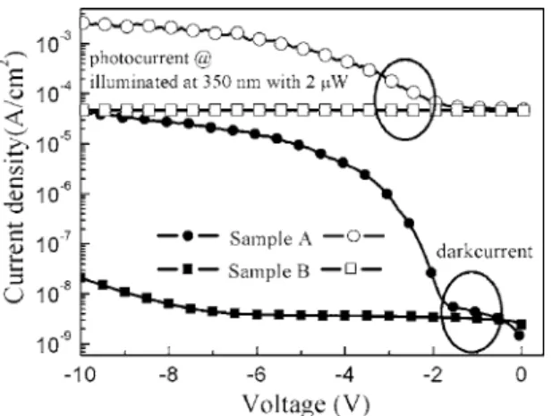
Figure 2 shows the typical I-V characteristics of the AlGaN/GaN p-i-n PDs taken in dark conditions and with illumination. The typi-cal dark current density of the inverted devices 共samples A兲 was below 5 nA/cm2at a reverse bias of below 2 V. However, one can see that the reverse dark current increases drastically up to tens of A when the reverse bias is larger than 5 V. The dark current is higher than the reported values observed from III-nitride p-i-n PDs.12In contrast, the typical dark current of samples B was less than 10 nA/cm2 even when the reverse biases were increased to
10 V. The higher dark current in samples A might be explained by the presence of trap levels within the bandgap of the samples giving rise to a high leakage current. These levels are most likely related to either process damage or to structural defects, including point de-fects. It is known that defects in GaN can reveal themselves in high leakage currents.13,14Because magnesium has a larger radius than gallium, it may incorporate as a substitutional and/or interstitial combination. Thus, high magnesium concentrations can be expected to degrade the crystal quality and the morphology of GaN.9In the inverted structures, after the growth of the p+-GaN layer, the
re-maining layers共i.e., undoped absorption layer and n+-AlGaN con-tact layer兲 could be grown on a poor p+-GaN surface resulting from
intense Mg doping. This process may lead to more structural defects in the inverted p-i-n structures共samples A兲 compared to the conven-tional structures共samples B兲. As shown in Fig. 2, samples B showed
a constant photocurrent共i.e., a near constant contrast of photocurrent to dark current兲 exhibiting a typical characteristic of p-i-n PDs. For samples A, it was found that the photocurrent showed a gradual increase as reverse biases were higher than 2 V. In fact, the typical reverse dark I-V curve also showed a step at a reverse bias of about 2 V, as shown in Fig. 2. The exact origin of this phenomenon is presently unknown. However, the probable cause may be a potential barrier that is associated with the p+-GaN/n+-GaN junction
hinder-ing carrier transport when a small reverse bias is applied to the inverted AlGaN/GaN p-i-n photodiodes. When the reverse bias volt-ages exceeded 2 V, carriers were transported by tunneling occurring in the p+-GaN/n+-GaN junction. Therefore, the photocurrent vs
ap-plied voltage curve included a step. Another possible origin of the I-V curve including a step observed in samples A might could be due to that the thin p-GaN buried layer was totally depleted, when the biased voltages exceeded 2 V, resulting in a carrier multiplication by avalanche process. Further studies to understand the exact origin are under way and relevant results will be published once available. Figure 3 shows the typical spectral responsivity of the AlGaN/GaN p-i-n PDs taken at different biases. Unbiased peak re-sponsivity of samples A was around 0.1 A/W at 350 nm corre-sponding to a quantum efficiency of around 35%. Similar peak value was also observed in samples B, as shown in the Fig. 3. However, as the incident wavelength was shorter that 350 nm, the responsivity of samples B decreased markedly with incident wavelength. The de-crease can be attributed to the significant surface absorption in the p-type graded AlxGa1−xN window layer and the p-type GaN contact layer when the wavelength of incident photons is shorter than 350 nm. In contrast, samples A with the n+-Al0.2Ga0.8N top contact
layer would have small surface absorption as the incident wave-length of photons is shorter than 350 nm. The zero-bias UV
Figure 1. Schematic device structure used
in this study.
Figure 2. Typical room-temperature I-V characteristics of the samples A and
samples B taken in dark and under illumination. The power and the wave-length of the incident light were 2W and 350 nm, respectively.
Figure 3. Typical spectral responsivity for the samples A and samples B
taken at different biases.
H183
Journal of The Electrochemical Society, 154共3兲 H182-H184 共2007兲 H183
共360 nm兲 to visible 共450 nm兲 rejection ratios extracted from the spectra response are around 30000, as shown in Fig. 3.
Based on the foregoing results, an inverted AlGaN/GaN p-i-n structure, including at least a p+/n++ tunneling junction, partially
solved the problem of the high-resistivity p-type AlGaN top contact layer in the conventional AlGaN-based UV photodiodes. In addi-tion, note that the processing procedures of the inverted nitride-based PDs are simpler than that of conventional nitride-nitride-based PDs. On the other hand, the responsivity increased with an increase of bias voltages for samples A, as shown in Fig. 3. For the below bandgap regions共i.e., incident wavelength ⬎365 nm兲, the increased responsivity could be attributable to the increase of dark current with bias voltages, as shown in Fig. 2. For the above bandgap re-gions共i.e., incident wavelength ⬍360 nm兲, the increased responsiv-ity could be attributable to the internal gain caused by material de-fects or carrier multiplication by avalanche process, as mentioned above. On the other hand, according to the I-V characteristics, one can deduce the zero-biased resistance area共R0A兲 product to give an
insight into the differences between these two samples. Typically, the R0A products were around 1⫻ 109⍀/cm2 and 2
⫻ 108⍀/cm2for samples A and samples B, respectively.
Concluding the study, we emphasize that AlGaN/GaN p-i-n pho-todiodes with inverted structure and a typical unbiased peak respon-sivity of 0.1 A/W at 350 nm, corresponding to a quantum efficiency of about 35%, were demonstrated. The typical dark current density of the inverted devices was below 5 nA/cm2 at a reverse bias of
below 2 V corresponding to a R0A value was around 1
⫻ 109⍀/cm2. Note that the responsivity of samples B decreased
markedly as the incident light wavelength共incident兲 is shorter than 350 nm. The decrease can be attributed to the significant surface absorption in the p-type graded AlxGa1−xN window layer and the
p-GaN contact layer. In the inverted devices共samples A兲, the short-wavelength 共incident⬍ 350 nm兲 responsivity did not show a
de-crease and were higher than those of samples B. This can be attrib-utable to the fact that the inverted p-i-n PDs have a low-resistivity and wide bandgap window layer.
Acknowledgments
The authors acknowledge the Center for Micro/Nano Technology Research, National Cheng Kung University, Tainan, Taiwan, for equipment access and technical support and the financial support from the National Science Council for their research grant of NSC 95-2221-E-006-354 and NSC 94-2221-E-218-051. The authors thank Professor Y. K. Su, Professor S. J. Chang, and Professor W. C. Lai for their useful suggestions on this work.
National Cheng-Kung University assisted in meeting the publication costs of this article.
References
1. D. Walker, E. Monroy, P. Kung, J. Wu, M. Hamilton, F. J. Sanchez, J. Diaz, and M. Razeghi, Appl. Phys. Lett., 74, 762共1999兲.
2. A. Osinsky, S. Gangopadhyay, R. Gaska, B. Williams, M. A. Khan, D. Kuksenkov, and H. Temkin, Appl. Phys. Lett., 71, 2334共1997兲.
3. G. Parish, S. Keller, P. Kozodoy, J. P. Ibbetson, H. Marchand, P. T. Fini, S. B. Fleischer, S. P. DenBaars, U. K. Mishira, and E. J. Tarsa, Appl. Phys. Lett., 75, 247 共1999兲.
4. V. Adivarahan, G. Simin, J. W. Yang, A. Lunev, M. A. Khan, N. Pala, M. Shur, and R. Gaska, Appl. Phys. Lett., 77, 863共2000兲.
5. J. C. Carrano, D. J. H. Lambert, C. J. Eiting, C. J. Collins, T. Li, S. Wang, B. Yang, A. L. Beek, R. D. Dupais, and J. C. Campbell, Appl. Phys. Lett., 76, 924共2000兲. 6. J. M. van Hove, R. Hickman, J. J. Klaassen, P. P. Chow, and P. P. Ruden, Appl.
Phys. Lett., 70, 2282共1997兲.
7. G. M. Smith, J. M. Redwing, R. P. Vaudo, E. M. Ross, J. S. Flynn, and V. M. Phanse, Appl. Phys. Lett., 75, 25共1999兲.
8. E. Monroy, M. Hamilton, D. Walker, P. Kung, F. J. Sánchez, and M. Razeghi, Appl. Phys. Lett., 74, 1171共1999兲.
9. J. K. Sheu and G. C. Chi, J. Phys.: Condens. Matter, 14, R657共2002兲. 10. D. J. H. Lambert, M. M. Wong, U. Chowdhury, C. Collins, T. Li, H. K. Kwon, B.
S. Shelton, T. G. Zhu, J. C. Campbell, and R. D. Dupuis, Appl. Phys. Lett., 77, 1900共2000兲.
11. S. R. Jeon, Y.-H. Song, H.-J. Jang, G. M. Yang, S. W. Hwang, and S. J. Son, Appl. Phys. Lett., 78, 3265共2001兲.
12. N. Biyikli, I. Kimukin, O. Aytur, and E. Ozbay, IEEE Photon. Technol. Lett., 16, 1718共2004兲; and references therein.
13. P. Kozodoy, J. P. Ibbetson, H. Marchand, P. T. Fini, S. Keller, J. S. Speck, S. P. DenBaars, and U. K. Mishra, Appl. Phys. Lett., 73, 975共1998兲.
14. E. G. Brazel, M. A. Chin, and V. Narayanamurti, Appl. Phys. Lett., 74, 2367 共1999兲.
H184 Journal of The Electrochemical Society, 154共3兲 H182-H184 共2007兲
H184