Chapter 2
Design and Analysis of the Novel Sensor Using Si Nanopillars array-Based Photonic Crystals
As mentioned in Chapter 1, the integrated development of optical sensor devices has become the future trend. We propose optical components for two-dimension (2-D) photonic crystals (PCs) sensor using silicon nanopillar array in this chapter. The content of chapter 2 is arranged as follows: Section 2-1 introduces the advantages of Photonic Crystals (PCs) applied in integrated optics are discussed and the background of the sensor.
It introduces classical materials for application in Section 2-2. In Section 2-3, working principle of the high sensitive sensor using Si-Nanopillar Array is introduced. Background theorem of Beam Propagation Method (BPM) and Finite Difference Time Domain (FDTD) Method and Plan Wave Expansion (PWE) are also briefly derived and discussed in Section 2-4. The various analysis of 2-D silicon nanopillars array with cubic and
hexagonal lattice of several shapes are compared based on computer-aided finite-difference time-domain (FullWAVE/FDTD) in Section 2-5. Finally, we give the summary in Section 2-6.
2-1 Introduction of the background
During the last 25 years, global research and development on the field of sensors has expanded exponentially in terms of financial investment, the published literature, and the number of active researchers. It is well known that the function of a sensor is to provide information on our physical, chemical and biological environment. Thus, a near revolution is apparent in sensor research, giving birth to a large number of sensor devices for medical technology and biotechnology. A biosensor furnishes information about its biotechnology and consists of a physical transducer and a biotechnology selective layer [21]. A biosensor contains a biological entity such as antibody, bacteria, bacillus, etc. as recognition agent, whereas a sensor does not contain these agents. The current tendency to carry out field monitoring has driven the development of biosensors as new analytical tools able to provide fast, reliable, and sensitive measurements with lower cost; many of them aimed at on-site analysis Biosensors can be also a defense tool through the early detection of hazardous materials such
as germs. Sensor devices have been made from classical semiconductors, solid electrolytes, insulators, metals and catalytic materials.
In the last years the interest for nanosensors has drastically grown thanks to their low cost, small dimensions, easy integration. At the same time, the development of nanotechnologies allowed the possibility to fabricate photonic crystals (PCs) structures [22-24], periodic patterns that can control and guide the photons by tailoring the transmission and reflection properties in specific direction and wavelength range.
2-2 Introduction Classical Materials for Application
Over the years, many types of sensors have been developed to identify and quantify the physics or biological materials. Depending on the targeted area from environmental monitoring to biomedical applications the constraints on a biosensor will be different. However, sensitivity, efficiency, miniaturization, manufacturability, latency, and cost-effectiveness are usually commonly desired features. There are varieties of recently proposed biosensors utilizing different configurations. Photonic crystals (PCs) have numerous potential applications in optics to implement both active and passive devices as well as linear and nonlinear devices. Dielectric particles
such as II-VI or III-V groups of nanometer-sized semiconductor materials, e.g. GaAs, CdSe, SiO2 and TiO2 are the most popular photonic crystals (PCs) materials [25]. Photonic crystals have been used in a wide range of applications such as 90° bend waveguides, filters, lasers, amplifiers, resonators, non linear devices [26]. Recently, photonic crystals (PCs) sensor have attracted attention for physics and biological sensing. Their application as sensors is a recent research field which seems to be very promising due to their extreme miniaturization, polarization sensitivity and MEMS integration.
2-2-1 Introduction of the Sensor
These devices have recently become popular for research in biological and chemical sensing as the demand for compact devices to detect biomolecules has increased. Because their chemical and physical properties may be tailored over a wide range of characteristics, the use of photonic crystals (PCs) are finding a permanent place in sophisticated electronic measuring devices such as sensors. During the last 10 years, photonic crystals (PCs) have gained tremendous recognition in the field of artificial
sensor in the goal of mimicking natural sense organs [27]. Better selectivity and rapid measurements have been achieved by replacing classical sensor materials with photonic crystals involving nano-technology and exploiting either the intrinsic or extrinsic functions of polymers. Semiconductors, semiconducting metal oxides, solid electrolytes, ionic membranes, and organic semiconductors have been the classical materials for sensor devices [28]. In this chapter, we design the sensor which it has small size, low cost, and potential for high sensitivity make them attractive for biosensing applications. Finally, current trends in sensor research and also challenges in future sensor research are discussed.
2-2-2 Advantages of the Sensor Using Si-Nanopillar Array
In the last few years, the study of photonic crystals (PCs) has intensified. Since the period of the photonic crystals (PCs) structures is generally shorter than the wavelength of the electromagnetic waves, the size of the photonic crystals (PCs) devices operating at the wavelengths in visible and infrared regions is in the scale of micrometers. Therefore, the photonic crystals (PCs) devices can be very compact. This property results in the potential to use the photonic crystals (PCs) structures to replace the
integrated optics devices in optical fiber communication systems. Hence, to utilize photonic crystals special dispersion relations and photonic bandgap (PBG) to realize optical devices in integrated optical circuits are attractive research topics in the recent years. Many different photonic crystals (PCs) were constructed from high-refractive-index materials. One of these materials is silicon. The combination of the high refractive index ( ~ 3.5 in the near infrared) and well-developed nano-fabrication methods make Silicon very promising for the construction of photonic crystals (PCs) [29-32]. Significant progress in the construction of two-dimensional photonic crystals (PCs) of Silicon has been made. Silicon is the dominant material in semiconductor industry to date. Because the refractive index of silicon is 3.5, the 2-D or 3-D photonic crystals photonic bandgap (PBG) is easy forming. Using Silicon wafer which is less expensive, low cost has better thermal conductivity and high quality optical fiber communication system in the range of 850-1550 nm be realized. Photonic crystals (PCs) are easy to compact with integrated circuit owing to well technique of semiconductor fabrication.
2-3 Principle of the High Sensitive Sensor Using Si-Nanopillar
Array
In order to make the photonic crystals (PCs) with periodic permutation with refracting rate of material or dielectric constant changing in the miniature structure. The PCs structure wills similar electron among the solid state crystal to produced photon energy. In this kind of photonic crystals (PCs), the characteristic of the electromagnetic wave including amplitude, phase place, leaning towards polarized direction and wavelength can get enormously different results by controlling the light frequency spectrum, group velocity chromatic dispersion and phase matching. PCs is biosensing because of the peculiar properties of PCs such as the capability of enhance electromagnetic waves interaction and control over the group velocity.
2-3-1 Characteristics and Appearance of the Photonic Crystals
Periodic dielectric structures are often referred to as photonic crystals.
PCs is structure where the refractive index is a periodic function in space.
The PCs structure wills similar electron among the solid state crystal to produced photon energy. In electronic semiconductors like Si, InP or GaAs the bandstructure for the electrons arises from the periodic arrangement of the atoms that make up the crystal lattice. Electron waves traveling through
the electronic semiconductor are scattered at the periodic electrostatic potentials of the atoms and their interference leads to the replacement of the free electron dispersion relation
( ) ( )
m k k
Efree
2
2 2v v h
= by the electronic band structure [33]. In PCs the photonic band structure results from scattering and interference of electromagnetic waves at periodic arrangements of materials with different refractive indicesn= ε , where
ε is the materials dielectric constant. The photonic band structure replaces the dispersion relation of photons k
n c v
⎟⎠
⎜ ⎞
⎝
=⎛
ω in a homogenous
dielectric medium with refractive index n and frequency ω along the direction , where c is the speed of light in vacuum. The photonic band structure depends on several parameters. One important parameter is the geometry of the lattice of the photonic crystals such as hexagonal or square lattice. Assuming that the diameter of the air pores does not change along the z-axis, such a structure is called two-dimensional (2D) photonic crystals (PCs). If the pore diameter is varied along the z-axis in such a way, that there is in addition to the periodicity in the x-y-plane also a periodicity along the z-direction, such a structure would be called a three-dimensional (3D) photonic crystals [34]. The light waves propagate in a structure of the periodically refractive index or electrical permittivity material. The light
kv
waves would be scattered in the periodically medium and so can't propagate in the periodically medium. This condition we call photonic bandgap (PBG) structure [35]. In this kind of photonic crystal, the characteristic of the electromagnetic wave including amplitude, phase place, leaning towards polarized direction and wavelength can get enormously different results by controlling the light frequency spectrum, group velocity chromatic dispersion, phase matching.
2-3-2 Theory of the Polarization
The state of polarization (SOP) refers to distribute of light energy between the two-polarization modes. The reason of that the region is still termed single mode. It means these two-polarization modes have the same propagation constant. It is that ideally the region is a perfectly circularly symmetric region [36]. Thus, though the energy of a pulse is divided between these two-polarization modes, since they have the same propagation constant, it does not give rise to pulse spreading by the phenomenon of dispersion.
Polarization is a distinguishing feature of electromagnetic radiation describing the shape and the orientation of the locus of the electric field vector extremity as a function of time. The polarization state is transformed
when a lightwave passes through a medium or is reflected by an object.
The variations in the SOP of a lightwave enable one to characterize the system under consideration. The classical concept of polarized light represents the SOP of a lightwave as a function of evolution of its electric field vector E. If the vector describes a stationary curve during the observation or measurement time, the lightwave is called polarized lightwave, sometimes the polarized light has a systematic change and the track of the electric field is predictable. It is called non-polarized if the extremity of vector E has a random position, and the track of the electric field is unpredictable. The electric field vector of an electromagnetic monochromatic plane wave can be expressed in terms of three orthogonal components in the right-handed Cartesian coordinate system [37]. If light is assumed to progress in the z direction, the real instantaneous electric field vector can be written as:
( ) ( )
( ) ( )
( )
( )
⎥ ⎥
⎥
⎦
⎤
⎢ ⎢
⎢
⎣
⎡
+
− +
−
=
⎥ ⎥
⎥
⎦
⎤
⎢ ⎢
⎢
⎣
⎡
=
0 cos cos
, , ,
,
oy y yx x ox
z y x
P z k t E
P z k t E
t z E
t z E
t z E t
z
E ω
r ω
(2-1)
Px and Py are the instantaneous phases, and the ω means angular frequency.
While z = 0, Eq. 2-1 can be shortened as Eq. 2-2:
( ) ( )
( ) ( )
( ⎥ ⎦ ⎤
⎢ ⎣
⎡
+
= +
⎥ ⎦
⎢ ⎤
⎣
= ⎡
y oy
x ox
y x
P t E
P t E
t E
t t E
E ω
ω cos r cos
)
(2-2) We define the electric field phase difference between x-axis and y-axis as Delta δ as Eq. 2-3 belowx y
def
P P −
δ = (2-3)
where - 180o < δ ≤ 180o. The orientation of the electric field vector E depends on the sign of the relative phase δ. Usually, if sinδ< 0, the ellipse is termed right-hand i.e. the rotation is clockwise to an observer looking toward the light source. Then
< 0
<
− π δ Left - Circle Polarization π
δ <
<
0 Right-Circle Polarization
The light is modeled as a sinusoidal electromagnet of an oscillating electric field and an oscillating magnetic field propagate through space.
The magnetic field is always perpendicular to the electric field, we usually sketch just the electric field when visualizing the optical wave's oscillations.
The electric field is a vector, and can be written by E(r, t) =Exex+Eyey+Ezez, where ex, ey and ez are the unit vectors in x, y and z direction [38-42].
When we assume that direction of propagation as z for a time varying electric field, both the magnitude and the direction can vary with time. We assume the two linearly independent solutions of the wave equations for the electric field are polarized linearly along the x and y directions. Since these two directions are perpendicular to each other, the two solutions are said to be orthogonally polarized. Since the wave equations are linear and any linear combination of these two linearly polarized fields is also a solution.
Polarized light does not have to oscillate linearly in a plane. It can move in more complicated patterns. For example, if the two oscillating electromagnetic waves that they can add to waveform a composite wave. In most cases, only a certain percentage of the signal is polarized, and the DOP (degree of polarization) gives the percentage of polarization compared to the total average power of the optical signal [43]. That definition of DOP is following the equation (2-4):
(2-4)
% 100 (%)
) (
) (
)
( ×
= +
d unpolarize polarized
polarized
Power Power
Power
DOP
2-3-3 Working Principle of the Sensor Using Si-Nanopillar Array
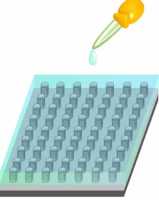
The presence of bio-molecules again contributes to a slightly change of refractive index, leading to an alteration of the optical transmission through the photonic crystals. Photonic crystals are very attractive for sensing applications because their properties are highly sensitive to changes in the refractive index in the nanopillars array. By the infiltration of bio-molecules photonic crystals structure caused by different group velocities of the polarization eigenmodes, it is shown in Fig.2-1. Therefore, in order to know the impairments of the variation state of polarization in the photonic crystals. We use the instruments of the polarimeter to measure polarization states to the impairments in the sensor. The electric field can be localized in the slight refractive index region, which makes the sensors extremely sensitive to the refractive index slight change resulting from the infiltration of bio-molecules. The focus for our research is to detect the strongly polarization sensitivity of the photonic crystals. We judge the bio-molecules from the slight different changes of refractive index, which caused photonic crystals strongly polarization sensitivity.
2-4 Background Theorem of Beam Propagation Method (BPM), Finite Difference Time Domain (FDTD) Method and Plan Wave Expansion (PWE) Method
In this section, our discussions were focused on the theorem that we used to calculate the integrated optical sensor characteristics. The analysis of PCs has been performed by various numerical approaches. The Beam Propagation Method (BPM), Finite Difference Time Domain (FDTD) method, and Plan Wave Expansion (PWE) method are widely used techniques for the investigation of PCs. Their strengths and weaknesses compared to each other are as follows. The full vector nature of the EM field has to be kept to accurately analyze the strongly modified dielectric materials as the scalar-wave approximation does not produce accurate results. By means of different mathematical methods to simulate different structure, the result will be more accurate. Before we fabricate the sensor devices, it is necessary to modeling and optimizing the parameters such as geometry, wavelength, material data, and output transmittance rate, etc.
According to the analysis of the result, it can obtain some information to correct the structure for better performance. So we design and simulate the
high performance optical biosensor devices based on beam propagation method, Finite Difference Time Domain (FDTD) method, and Plan Wave Expansion (PWE) method which was one of the most popular approaches used in the modeling and simulation of electromagnetic wave propagation in fiber-optic devices. They are mathematical methods and usually being used to simulate numerically for a general optical integrated circuit.
2-4-1 Mathematical Formulation of Beam Propagation Method
By using different mathematical methods to simulate different waveguide structure, the result will be more accurate. Before we fabricate the waveguide devices, it is necessary to modeling and optimizing the parameters such as geometry, wavelength, material data, and output field distribution, etc. According to the analysis of the result, it can obtain some information to correct the waveguide structure for better performance.
2-4-1-1 Forward Beam Propagation Method
The beam propagation method (BPM) is the most powerful technique
z z+Δz
to investigate the condition of the light wave propagation in various waveguides. Several kinds of BPM procedures are fast Fourier transform BPM (FFT-BPM) and finite difference BPM (FD-BPM) [44-45]. They are based on fundamental theory and calculation step by step. It calculates the optical field within one propagation step along the longitudinal coordinate to . The electric and magnetic field derived from the Maxwell’s equation can be represented as
t E B
∂
−∂
=
×
∇
v v (2-5)
t J D
H ∂
+∂
=
×
∇
v v
v (2-6)
(2-7) (2-8) where
=0
⋅
∇ Dv
=0
⋅
∇ Bv
Ev is the intensity of the electric field, Bv is the flux density of the magnetic field, Dv is flux density of the electric field, Hv is intensity of magnetic field and is electric current density. In a source-free Maxwell’s equation , we substitute Eqs. (2-6) into (2-5) and assume the time-dependence factor that exhibited here is
Jv
=0 Jv
)
exp(jωt , where ω is the angular-frequency. Then we obtain
E k n E E
E
Ev v 2 v 2 v 2 2 v
)
(∇⋅ −∇ = =
∇
=
×
∇
×
∇ μεω (2-9)
where k =ω ε0μ0 is the wave number in vacuum, is the refractive index, where
n
ε0 and μ0 are the dielectric constants and permeability coefficient in free space, respectively. The scalar filed assumption allows the wave equation to be written in the form of the Helmholtz equation, which is the basis of BPM, is expressed by
0 )
, ,
( 2
2 2 2 2 2
2 + =
∂ +∂
∂ +∂
∂
∂ k x y z E
z y x
φ φ
φ (2-10)
The scalar electric field has been written as , and the has been introduced for the spatially dependent wavenumber. Here
t
e i
x y x t
z y x
E( , , , )=φ( , , ) −ω )
, , ( ) , ,
(x y z k0n x y z
k =
λ π 2
0 =
k is the wavenumber in free space and is the refractive index distribution. We separate the electric field
) , , (x y z n
) , , (x y z φ
into two parts: the axially slowly varying envelope term of and rapidly varying term of
) , , (x y z u )
exp( zikv . Then, φ(x,y,z) is expressed as )
exp(
) , , ( ) , ,
(x y z u x y z ikvz
φ = (2-11) where kv is a constant number and
n k kv v
= 0 , nv is reference refractive index. Substituting Eq. (2-11) into Eq. (2-10), we obtain
0 ) (
2 22 22 2 2
2
2 + − =
∂ +∂
∂ +∂
∂ + ∂
∂
∂ k k u
y u x
u z k u z i
u v v (2-12)
Assumption the variation of with is sufficiently slow so that the first term above can be neglected with respect to the second. With assumption
u z
and after slight rearrangement, the above equation is expressed as
⎟⎟⎠
⎜⎜ ⎞
⎝
⎛ + −
∂ +∂
∂
= ∂
∂
∂ k k u
y u x
u k i z
u ( )
2
2 2 2 2
2 v
v (2-13)
The equation (2-13) is the basic formulate for BPM simulations.
2-4-2 Mathematical Formulation of Finite Difference Time Domain Method
In this section, the numerical method, FDTD is used to calculate the EM field distributions in two-dimensional photonic crystals. The FDTD method is a direct solution of Maxwell’s time-dependent curl equations. It replaces the spatial and temporal derivatives of these equations with finite-difference expressions [46]. The approach gives explicit solutions to the time-domain electric- and magnetic-field within the computational volume under analysis without complicated computations. This gives the advantage that complicated structures may be calculated easily. Given its time-domain nature, solutions are broadband, and quantities may be easily transformed to the frequency domain utilizing the discrete Fourier transform (DFT). On the boundaries of computational volume, reflection of unphysical EM wave will occur because of the discontinuity. In order to solve this difficulty, Berenger’s perfectly matched layer (PML) is introduced, PML is a range in computational volume, and it can reduce the
reflections that causes by the incident wave propagated into PML layers [47]. In 1966 Yee proposed this technique to solve Maxwell’s curl equations [48]. Yee’s method has been used to solve numerous scattering problems on microwave circuits and dielectrics at microwave frequencies.
Because this method needs great demand of computing resources, this method was not popular in the past. However, with the low cost, powerful computers, the FDTD technique has become a popular method for solving EM wave problems
2-4-2-1 Mathematical Formulation of Finite Difference Time Domain Method
The finite difference time domain (FDTD) method is the most powerful technique to investigate the condition of the light wave propagation in various waveguides. A well-known method in the study of electromagnetic wave scattering and radiation is the finite difference tine domain (FDTD) method [49-50]. The FDTD method is used to solve the Maxwell’s time-dependent curl equations numerically. The time-dependent and Maxwell’s equation is expressed by (2-5), (2-6), (2-7) and (2-8).
Bv and Dv can be expressed as In linear and isotropic materials, the
H
Bv =μv (2-14) (2-15) where
E Dv =εv
μ is magnetic permeability, and ε is electrical permittivity. We substitute Eqs. (2-14) and (2-15) into Eqs. (2-5) and (2-6), then the Maxwell’s curl equations as
) 1(
t E
Hv v
×
∇
−
∂ =
∂
μ (2-16) J
t H
Ev v v
ε ε
) 1 1(
−
×
∇
∂ =
∂ (2-17)
In a rectangular coordinate system, Eqs. (2-16) and (2-17) are equivalent to the following system of scalar equations:
⎥⎦
⎢ ⎤
⎣
⎡
∂
−∂
∂
= ∂
∂
∂
y E z E t
Hx y z
μ
1 (2-18)
⎥⎦⎤
⎢⎣⎡
∂
−∂
∂
= ∂
∂
∂
z E x E t
Hy z x
μ
1 (2-19)
⎥⎦
⎢ ⎤
⎣
⎡
∂
−∂
∂
= ∂
∂
∂
x E y E t
Hz x y
μ
1 (2-20)
x z y
x J
z H y H t
E
ε ε
1
1 ⎥−
⎦
⎢ ⎤
⎣
⎡
∂
−∂
∂
= ∂
∂
∂ (2-21)
y z
y x
x J H z H t
E
ε ε
1
1 −
⎥⎦⎤
⎢⎣⎡
∂
−∂
∂
= ∂
∂
∂ (2-22)
z y x
z J
y H x H t
E
ε ε
1
1 ⎥−
⎦
⎢ ⎤
⎣
⎡
∂
−∂
∂
= ∂
∂
∂ (2-23)
Now we denote a grid point of the space is represented by
) , , ( ) , ,
(i j k = iΔx jΔy kΔz (2-24) and a field functions of space and time is expressed by [51]
) , , ( ) , , , ( ) , ,
(x y z u i x j y k z n t u i j k
u = Δ Δ Δ Δ = n (2-25) where , i j, k and are integers, n Δx , Δy , and Δz are the space increments in the x, y and z coordinate directions, and is the time increment. Consider this expression for the first space derivative of in the x-direction and it is evaluated at the fixed time
Δt
u
t n
tn = Δ is expressed as
x
k j i
u k j i
u t n z k y j x x i
u n n
Δ
−
−
= + Δ Δ Δ
∂ Δ
∂ ( 12, , ) ( 12, , )
) , , ,
( (2-26)
The expression for the first time partial derivative of and it is evaluated at the fixed space point
u
) , , (i j k
t
k j i u k j i t u
n z k y j x x i
u n n
Δ
= − Δ Δ Δ
∂ Δ
∂ + (, , ) − (, , )
) , , ,
( 2
2 1 1
(2-27) For Eq. (2-18) we have
t
k j
i H k
j i
Hxn xn
Δ
+ +
− +
+ −
+12(, 12, 12) 12(, 12, 12)
⎥⎥
⎦
⎤
⎢⎢
⎣
⎡
Δ
+
− +
− +
⎥⎥
⎦
⎤
⎢⎢
⎣
⎡
Δ
+
− +
= +
y
k j i E k
j i E z
k j
i E k
j i
Eny(, 12, 1) yn(, 12, ) 1 zn(, 1, 12) zn(, , 12) 1
μ μ
(2-28) The finite difference equations are corresponding to Eqs. (2-19) and (2-20),
For Eq. (2-21) we have
t
k j i
E k j i
Exn xn
Δ
+
−
+12, , ) − ( 12, , )
( 1
⎥⎥
⎥
⎦
⎤
⎢⎢
⎢
⎣
⎡
Δ
− +
− +
= +
−
−
y
k j
i H k j
i
Hzn ( 12, 12, ) zn ( 12, 12, )
1 2
2 1 1
ε
⎥⎥
⎥
⎦
⎤
⎢⎢
⎢
⎣
⎡
Δ
− +
− +
− +
−
−
z
k j i
H k
j i
Hyn ( 12, , 12) ny ( 12, , 12)
1 2
2 1 1
ε
) , 2, ( 1
12
k j i
Jxn +
+ − (2-29) the finite difference equations are corresponding to Eqs. (2-22) and (2-23), respectively. They also can be similarly constructed. The grid points for E-components and H-components are used to approximate the condition as shown in Fig. 2-2.
We will mathematical formulation of two-dimensional photonic bandgap structure. The light waves propagate in a structure of the periodically refractive index or electrical permittivity material. The intensity of the certain light waves would be decreased exponentially from the destructiveness interference. Due to the light waves would be scattered in the periodically medium and so can’t propagate in the periodically medium [52-54]. The light wave propagate in a periodically electrical permittivity material, the light wave would be abided by the Maxwell’s
equation. The Maxwell’s equation is expressed by (2-5), (2-6), (2-7) and (2-8). We assume all materials are linear, lossless and isotropic, then (2-5) and (2-6) could be expressed by
H t i
E Bv v
v
ωμ0
∂ =
−∂
=
×
∇ (2-30) E
r t i
H Dv v v
v =−ϖε0ε( )
∂
= ∂
×
∇ (2-31) In linear, lossless and isotropic materials, the Bv and Dv can be expressed as
H Bv v
μ0
= (2-14)
E r
Dv v v
)
0ε( ε
= (2-15) where ε(rv) is the dielectric function and it is the square of the refractive index. The time independent solutions is expressed by
t
e i
r E r
E(v)= ( ) −ω (2-32) (2-33) We substitute Eqs. (2-32) and (2-33) into Eqs. (2-30) and (2-31), then the Maxwell’s curl equations to obtain the vector Helmholtz equation
t
e i
r H r
H(v)= ( ) −ω
) ( )
) ( (
1 2
r c H r
r H
v
v v ⎟
⎠
⎜ ⎞
⎝
=⎛
⎥⎦
⎢ ⎤
⎣
⎡ ∇×
×
∇ ω
ε (2-34) According to the Bloch’s theorem, we obtain the solution of H v(r) and it is
k t r k
i h
e r
Hv v (vv )vv )
( = ⋅ −ω (2-35) where hvkv
is a periodicity function of the lattice structure. We substitute Eqs. (2-35) into (2-34), then we obtain [55]
( ) ( )
k k kk h h
h c k r i
k i h
L v v v vv vv vv
v v v
v 2 2
) (
ˆ 1 ω ω
ε ⎟⎠ =
⎜ ⎞
⎝
=⎛
× +
∇
× +
∇
= (2-36)
where Lˆ is the operator, is the velocity of light, c ω is the frequency of angle, kv is the wavevector,
hvkv
is the eigenvector, and ω is the eigenvalue. Due to the relation of the functions of ω and , we can obtain the bandgap structure in the
k
−k
ω plane surface.
2-4-3 Plan Wave Expansion (PWE) Method
Plan wave expansion (PWE) [56] method is commonly used for photonic crystal related researches. The dispersion relation of the periodically arranged dielectric structure it is also called band structure–
can be obtained by this method. According to the band structures, many useful information could be extracted, such as PBG, phase velocity, and energy velocity, and so on.
To derive the equations of the PWE method, we start from Maxwell’s equations.
t H c t
B E c
∂
− ∂
∂ =
− ∂
=
×
∇
v
v 1 v μ
t E c t D H c
∂
= ∂
∂
= ∂
×
∇
v
v 1 v ε
(2-37)
(2-38)
Taking time-independent solutions Eqs. (2-32) and (2-33)
t
e i
r E r
E(v) = ( ) −ω
t
e i
r H r
H(v) = ( ) −ω
the Helmholtz equation is
( ) ( ) ( ) ( )
H rc r r
r H
v v v v
v 2
1 ω2μ
ε ⎟⎟⎠=
⎜⎜ ⎞
⎝
⎛ ∇×
×
∇ (2-39)
then using Block’s theorm
( ) ( )
r u r ei( )k rH v
v v
v = • (2-40)
where u v(r) is a function with the periodicity of the lattice.
Inserting this expression in the Helmholtz equation, we obtain
( ) ( )( )
k kk ik u u
ik r u
Jˆ 1 ω2
ε v ⎟⎟⎠× = v
⎜⎜ ⎞
⎝
⎛ +∇
×
∇ +
= (2-41)
ωv is the normalized frequency, and is the operator we defined. Eqs.
(2-41) is the fundamental equation solved by plane wave expansion.
Jˆ
ωv is eigenvalue, uk is eigenvector, and k is a free parameter. By solving ωvin suitable path in the first Brillouin zone, a band structure can be obtained
2-5 Compare and Analysis of the High Sensitive Sensor
The design of sensor is based on the period structure of photonic crystal. The period structure of photonic crystal with different liquid filling, the slightly difference of refractive index, will change photonic crystals (PCs) properties, including polarization, transmittance and phase matching.
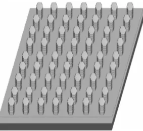
In this chapter, we adopt the computer-aided finite-difference time-domain (FullWAVE/FDTD) software [58-59] based on BeamPROP_CAD [60] to simulate the size of optical sensor. And different arranging is discussed, such as cubic arranging, hexagonal arranging. After the compare of two kinds of arranging, our optical sensor will be based on the optimal arranging we chosen. Following analysis is comparison various kinds of structure with the same parameter, materials used silicon, pillar radius is about 100 nm with period 250 nm. The optical sensor fabrication will be described in the next Chapter.
2-5-1 Compare and Analyze of Various Structures based on Cubic Arranging
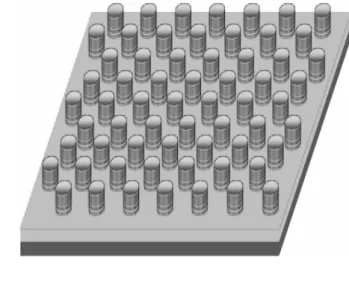
The cubic arranging structures of cylinder, hexagon and square pillar
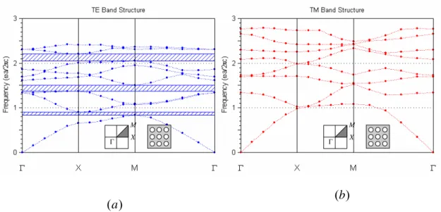
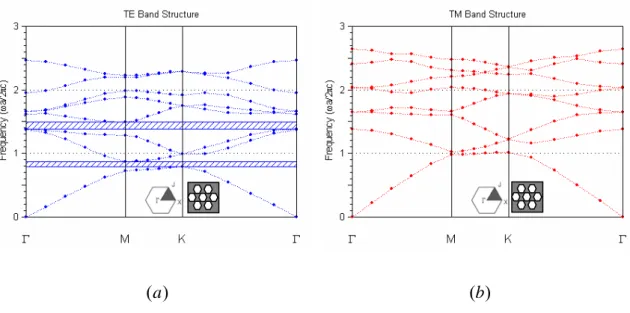
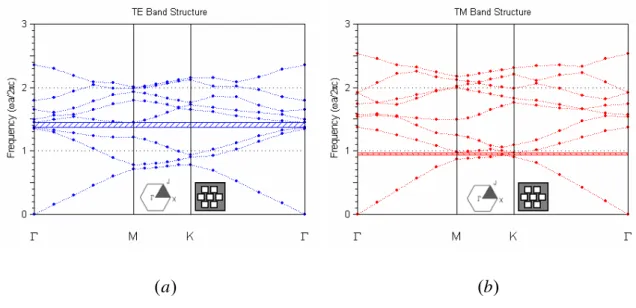
are analyzed and compared below. Fig. 2-3 shows cubic arranging structures of cylinder pillar. Fig. 2-4 shows that TE mode and TM mode Photonic Band Gap (PBG) in cylinder respectively. Fig. 2-5 shows cubic arranging structures of hexagon pillar. Fig. 2-6 show that TE mode and TM mode Photonic Band Gap (PBG) in hexagon respectively. Fig. 2-7 shows cubic arranging structures of square pillar. Fig. 2-8 show that TE mode and TM mode Photonic Band Gap (PBG) in square respectively.
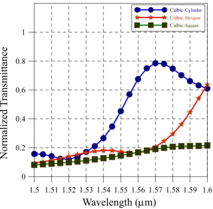
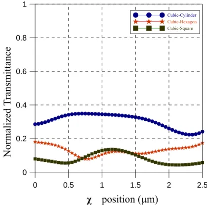
It is an optical communication time now so optical sensor is applied to the optical communication system hopefully. And it is set a monitor point at receiver of the sensor assembled in various structures, Fig. 2-9 shows that it has the best transmittance in cylinder arranging at TE mode for 1.55 μm of wavelength. And Fig. 2-10 shows that it has the best transmittance in hexagon arranging at TM mode for 1.55 μm of wavelength.We take 1.55 μm wavelength of light as incident light and set x-axis at receiver port to monitor the change of transmittance as shown Fig. 2-11. It shows that it has the best transmission and uniform transmittance density in cylinder for TE mode in Fig. 2-12. And it shows that it has the best transmittance at x-axis and uniform transmittance density in hexagon for TM mode in Fig. 2-13.
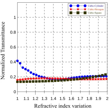
And utilize the sensor to soak in the solution of sample and come to do the Simulation and analysis as shown Fig.2-14. We monitor the change of transmittance by adjusting refractive index slightly. Because refractive index of liquid or lived being’s DNA is about between 1 and 2, it can be simulated the transmittance in such a refractive index range. Fig. 2-15 showed that transmittance in cylinder arranging for TE mode is the largest and has the largest response according to the change of refractive index.
And the transmittance for TM mode is the largest and has largest change according refractive index in cylinder or square rod showed in Fig. 2-16.
2-5-2 Compare and Analyze of Various Structures based on Hexagonal Arranging
The hexagonal arranging structures of cylinder, hexagon and square pillar are analyzed and compared below. Fig. 2-17 shows hexagonal arranging structures of cylinder pillar. Fig. 2-18 shows that TE mode and TM mode Photonic Band Gap (PBG) in cylinder respectively. Fig. 2-19 shows hexagonal arranging structures of hexagon pillar. Fig. 2-20 show that TE mode and TM mode Photonic Band Gap (PBG) in hexagon
respectively. Fig. 2-21 shows hexagonal arranging structures of square pillar. Fig. 2-22 show that TE mode and TM mode Photonic Band Gap (PBG) in square respectively.
It is an optical communication time now so optical sensor is applied to the optical communication system hopefully. And it is set a monitor point at receiver of the sensor assembled in various structures, Fig. 2-23 shows that it has the best transmittance in cylinder arranging at TE mode for 1.55 μm of wavelength and it is the same for TM mode showed in Fig. 2-24. We take1.55 μm wavelength of light as incident light and set x-axis at receiver port to monitor the change of transmittance as shown Fig. 2-25. It shows that it has the best transmission and uniform transmittance density in cylinder for TE mode in Fig. 2-26. And it shows that it has the best transmittance at x-axis and uniform transmittance density in cylinder for TM mode in Fig. 2-27. And utilize the sensor to soak in the solution of sample and come to do the Simulation and analysis as shown Fig.2-28. We monitor the change of transmittance by adjusting refractive index slightly.
Because refractive index of liquid or lived being’s DNA is about between 1 and 2, it can be simulated the transmittance in such a refractive index
Fig. 2-29 showed that transmittance in cylinder arranging for TE mode is
the largest and has the largest response according to the change of refractive index, the relation of refractive index and transmittance is linear.
And the transmittance for TM mode is the largest and has largest change according refractive index in cylinder or square pillar showed in Fig. 2-30.
2-6 Summy
According to the various analysis of 2-D silicon array with cubic and hexagonal lattice of several shapes are compared in this chapter. The several shapes are included cylinder, square and hexagon. The author will make some discussions and conclusions in follow texts. Accord to compare and analysis of the various structures in section 2-5, Fig. 2-31 shows that it has the best transmission in hexagonal structures of cylinder arranging at TE mode for optical communication always used 1.55 μm of wavelength and it is the same for TM mode showed in Fig. 2-32. We take 1.55 μm wavelength of light as incident light and set x-axis at receiver port to monitor the change of transmittance. It shows that it has the best transmittance and uniform transmittance density in hexagonal structures of
cylinder arranging for TE mode in Fig. 2-33 and it is the same for TM mode showed in Fig. 2-34. And we monitor the change of transmission by adjusting refractive index slightly. From Fig. 2-35, Fig. 2-36, we can obtain the TE mode and TM mode has large change in refractive index in hexagonal structures of cylinder. There are linear relative in transmission and refractive curve. The grade difference of TE, TM mode curve in Fig.
2-37 show the trend of polarization. Our sensors were very sensitive. From the comparison of the results, hexagonal structures of cylinder are the best arrange of sensor design.
Fig. 2-1 Working Principle of the Sensor Using Si-Nanopillar Array
Hy
Ez
Hx
Hx
Hy
Hz
Hz
Ey
Hz
z
Hx
Ex
y
x (i, j,k)
Hy
Fig. 2-2Position of the electric and magnetic field vector components about a cubic unit cell of the Yee space lattice[51]
) ) (b
(a
Fig. 2-3 The cubic arranging structures of cylinder. (a) Vertical view (b) Side view
Γ X
M
Γ X
M
) ) (b
(a
Fig. 2-4 The cubic arranging structures of cylinder of (a) TE band
)
(a (b)
Fig. 2-5 The cubic arranging structures of hexagon. (a) Vertical view (b) Side view
Γ X
M
Γ X
M
)
(a (b)
Fig. 2-6 The cubic arranging structures of hexagon of (a) TE band structure, (b) TM band structure.
)
(a (b)
Fig. 2-7 The cubic arranging structures of square. (a) Vertical view (b) Side view
Γ X
M
Γ X
M
)
(a (b)
. 2-8 The cubic arranging structures of square of (a) TE band structure, (b)
1.5 1.51 1.52 1.53 1.54 1.55 1.56 1.57 1.58 1.59 1.6 0
0.2 0.4 0.6 0.8
Normalized Transmittance
Wavelength (μm)
Fig. 2-9 Simulation resules in cubic arranging structure at TE mode for 1.55 μm of wavelength.
1.5 1.51 1.52 1.53 1.54 1.55 1.56 1.57 1.58 1.59 1.6 0
0.2 0.4 0.6 0.8 1
Cubic-Cylinder Cubic-Hexgon Cubic-Square
Normalized Transmittance
Wavelength (μm)
Fig. 2-10 Simulation resules in cubic arranging structure at TM mode for 1.55 μm of wavelength.
0 2.5
0 2.5 0 2.5
LIGHT
LIGHT LIGHT
) ) (c
(a (b)
Fig. 2-11 We take1.55 μm wavelength of light as incident light and set x-axis at receiver port to monitor the change of transmittance, the cubic arranging structures of (a) cylinder (b) hexagon (c) square.
0 0.5 1 1.5 2 2.5
0 0.2 0.4 0.6 0.8 1
Cubic-Cylinder Cubic-Hexagon Cubic-Square
Normalized Transmittance
χ position (μm)
Fig. 2-12 Simulation resules that we take1.55 μm wavelength of light as
0 0.5 1 1.5 2 2.5 0
0.2 0.4 0.6
Normalized Transmittance
χ position (μm)
Fig. 2-13 Simulation resules that we take1.55 μm wavelength of light as incident light and set x-axis at receiver port to monitor the change of transmittance at TM mode.
Fig. 2-14 Utilize the cubic structure sensor to soak in the solution of sample and come to do the simulation and analysis.
Refractive index variation
Fig. 2-15 The change of transmittance by adjusting refractive index slightly at TE mode.
Fig. 2-16 The change of transmittance by adjusting refractive index
1 1.1 1.2 1.3 1.4 1.5 1.6 1.7 1.8 1.9 2 0
0.2 0.4 0.6 0.8
Normalized Transmittance
1 1.1 1.2 1.3 1.4 1.5 1.6 1.7 1.8 1.9 2 0
0.2 0.4 0.6 0.8 1
Cubic-Cylinder Cubic-Hexagon Cubic-Square
Normalized Transmittance
Refractive index variation
![Fig. 2-2 Position of the electric and magnetic field vector components about a cubic unit cell of the Yee space lattice[51]](https://thumb-ap.123doks.com/thumbv2/9libinfo/7101519.30443/32.892.173.724.641.1015/position-electric-magnetic-field-vector-components-cubic-lattice.webp)